Article

Design of Synaptic Driving Circuit for TFT eFlash-Based Processing-In-Memory Hardware Using Hybrid Bonding

1
Department of Electronic Engineering, Changwon National University, Changwon 51140, Republic of Korea
2
Department of Electrical and Computer Engineering, Seoul National University, Seoul 08826, Republic of Korea
3
Department of Electronic Engineering, Engineering Research Institute (ERI), Gyeongsang National University, Jinju 52828, Republic of Korea
4
Korea Institute of Science and Technology (KIST), Seoul 02792, Republic of Korea
*
Author to whom correspondence should be addressed.
Electronics 2023, 12(3), 678; https://doi.org/10.3390/electronics12030678
Submission received: 25 December 2022 / Revised: 12 January 2023 / Accepted: 21 January 2023 / Published: 29 January 2023

Abstract

:
This paper presents a synaptic driving circuit design for processing in-memory (PIM) hardware with a thin-film transistor (TFT) embedded flash (eFlash) for a binary/ternary-weight neural network (NN). An eFlash-based synaptic cell capable of programming negative weight values to store binary/ternary weight values (i.e., ±1, 0) and synaptic driving circuits for erase, program, and read operations of synaptic arrays have been proposed. The proposed synaptic driving circuits improve the calculation accuracy of PIM operation by precisely programming the sensing current of the eFlash synaptic cell to the target current (50 nA ± 0.5 nA) using a pulse train. In addition, during PIM operation, the pulse-width modulation (PWM) conversion circuit converts 8-bit input data into one continuous PWM pulse to minimize non-linearity in the synaptic sensing current integration step of the neuron circuit. The prototype chip, including the proposed synaptic driving circuit, PWM conversion circuit, neuron circuit, and digital blocks, is designed and laid out as the accelerator for binary/ternary weighted NN with a size of 324 × 80 × 10 using a 0.35 μm CMOS process. Hybrid bonding technology using bump bonding and wire bonding is used to package the designed CMOS accelerator die and TFT eFlash-based synapse array dies into a single chip package.

1. Introduction

Neural networks are widely used in various fields, such as regression analysis, pattern recognition, and clustering, thanks to their powerful performance [1,2,3,4,5]. Since numerous multiply accumulate operations and massive memory access for storing intermediate data and weights are required to process them in hardware, learning and inference of the neural network model have been performed using a cloud server. Recently, light-weighted neural network models have been developed that show little performance degradation when performing inference with quantized weights and activations [6,7,8] or using architectural design strategies with few parameters [9,10,11,12]. Therefore, energy-efficient hardware accelerators are being developed for edge computing that performs inference in the edge device instead of the data center, which provides advantages such as high responsiveness, reduced bandwidth cost, and data security.
Since the DRAM memory access energy is much greater than the computation energy, it is essential to minimize data movement to implement a high-energy-efficient accelerator for edge devices [13,14] Conventional Von Neumann structures have high design flexibility and high computational accuracy but show long latency and low energy efficiency due to massive data movement between memory and computing blocks [14,15,16,17]. Therefore, to solve this problem, a processing-in-memory (PIM) structure [18,19,20,21,22,23,24,25] has been proposed recently. The PIM structure can achieve high energy efficiency and low latency from low data movement and massively parallel operation using memory with a built-in computation function. As memory for synaptic weights, high-performance SRAM can be implemented with a standard CMOS logic process. However, due to the limitations of volatile memory, DRAM access can inevitably occur to write the pre-trained weights whenever the power of the edge device is turned on. Non-volatile memories such as RRAM [23,24,25] and embedded flash (eFlash) [26] can be used to solve this problem, but RRAM has the technical difficulties of implementing large-capacity memories and low program resistance values. So, when the PIM structure operates in current mode, it can consume significant power due to low program resistance and be sensitively affected by IR voltage drop due to parasitic resistance components of the layout.
Recently, hardware that applies a single thin-film transistor (TFT) eFlash device to a spiking neural network (SNN) has been reported [26], but it is not suitable for a deep neural network (DNN) because negative weight values cannot be programmed. Additionally, the process for TFT eFlash devices requires a high temperature (≥800 °C), so it is challenging to implement TFT eFlash devices after the standard CMOS logic process with aluminum metallization to fabricate monolithic 3D ICs. Furthermore, since the PIM structures typically employ analog processing instead of digital processing, eFlash device variations and mismatch can severely degrade inference accuracy when offline-learned synaptic weights are used in the hardware [20].
In this paper, we propose a TFT eFlash-based synaptic cell capable of programming negative weight values, a pulse-width modulation (PWM) conversion circuit for good linearity, and a synaptic array driving circuit that precisely programs the sensing current of the eFlash device into the target current (=50 nA ± 0.5 nA) using a program pulse train. In addition, hybrid bonding technology is proposed for single packaging of the proposed synaptic driving circuit die and the TFT eFlash-based synapse array die.

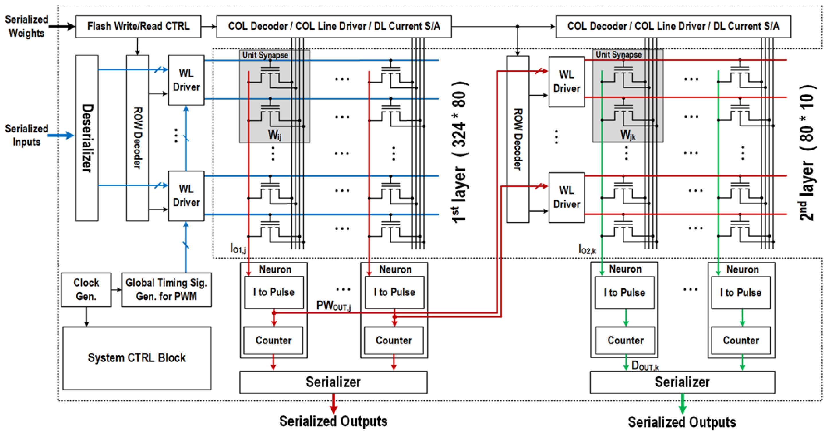
2. System Architecture

Figure 1 shows the overall block diagram of the TFT eFlash-based neural network accelerator. The prototype chip is designed as a binary/ternary weighted NN with a size of 384 × 80 × 10, considering the die size. The 1st and 2nd synapse arrays with a crossbar structure have sizes of 384 × 80 and 80 × 10, respectively. After erasing both eFlash synapse arrays for inference, the pre-trained synaptic weights are programmed into the first and second synapse arrays, respectively. The 8-bit input data is stored in each row of the first synapse array through the deserializer circuit and is converted into 256-level time information through PWM. Then, the converted pulses are transmitted to the word line (WL) of the first synapse array. That is, the input image x is processed to generate the jth intermediate output current Io1,j in the column direction of the first synapse array by the synaptic weight matrix WIJ stored in the first synapse array of 384 × 80 size as follows:
I o 1 , j = I c e l l × ( n = 1 384 ω n j × x n + b j ) ,   j ( 1 ,   2 ,   3 , ,   80 )
where Icell is the read current of the synapse, ωnj is the (n, j)th element of WIJ, xn is the nth pixel of x, and bj is the bias for Io1,j. The first neuron circuit receives Io1 and outputs a pulse for the input of the second synapse array of 80 × 10 size. The width of the output pulse PWOUT is proportional to the input current, and the rectified linear unit (ReLU) is used as an activation function for non-linear operation as follows:
P W O U T , j = max ( 0 ,   I o 1 , j M × I R E F ) ,   j ( 1 ,   2 ,   3 , ,   80 )
where M is the scaling factor, and IREF is the reference current used during conversion. The ReLU-processed PWOUT is processed to generate the kth output current Io2,k in the column direction of the second synapse array by the synaptic weight matrix WJK stored in the second synapse of 80 x 10 size as follows:
I o 2 , k = I c e l l × ( n = 1 80 ω n k × P W O U T , n + b k ) ,   k ( 1 ,   2 ,   3 , ,   10 )
where ωnk is the (n, k)th element of WJK, and bk is the bias for Io2,k. Io2 is converted to the 8-bit digital value by the second neuron circuit as
D O U T , k = A / D (   I o 2 , k M × I R E F ) ,     k ( 1 ,   2 ,   3 , ,   10 )
where A/D represents analog-to-digital conversion. DOUT is output through the serializer to obtain the final output value. As an activation function of the last layer, the proposed structure converts DOUT,k into a probability value Ok using the Softmax function for classification as
O k = e D O U T , k n = 1 10 e D O U T , n ,     k ( 1 ,   2 ,   3 , ,   10 )
In the prototype chip, the Softmax function is handled off the chip. The proposed architecture has three clock domains: a 4-phase 32-MHz clock for pulse width modulation of 8-bit digital input, an 8-MHz clock for system control, serializer, and deserializer, and an 8-kHz clock for erasing and programming the eFlash synapse arrays. Except for synaptic driving circuits and neuron circuits, digital blocks are designed using a hardware description language and synthesized with Auto placement and routing (PnR).

3. Circuit Description

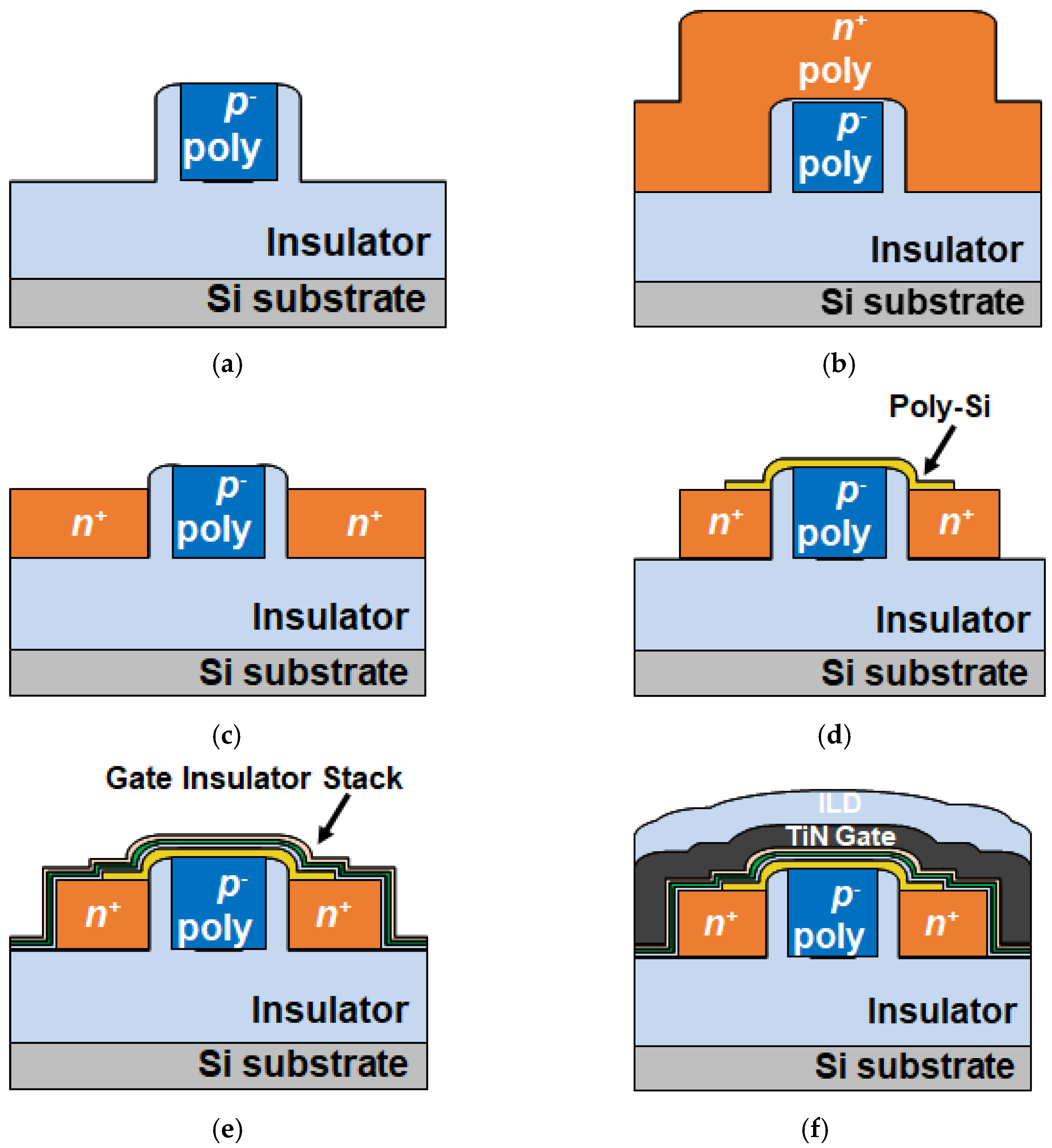
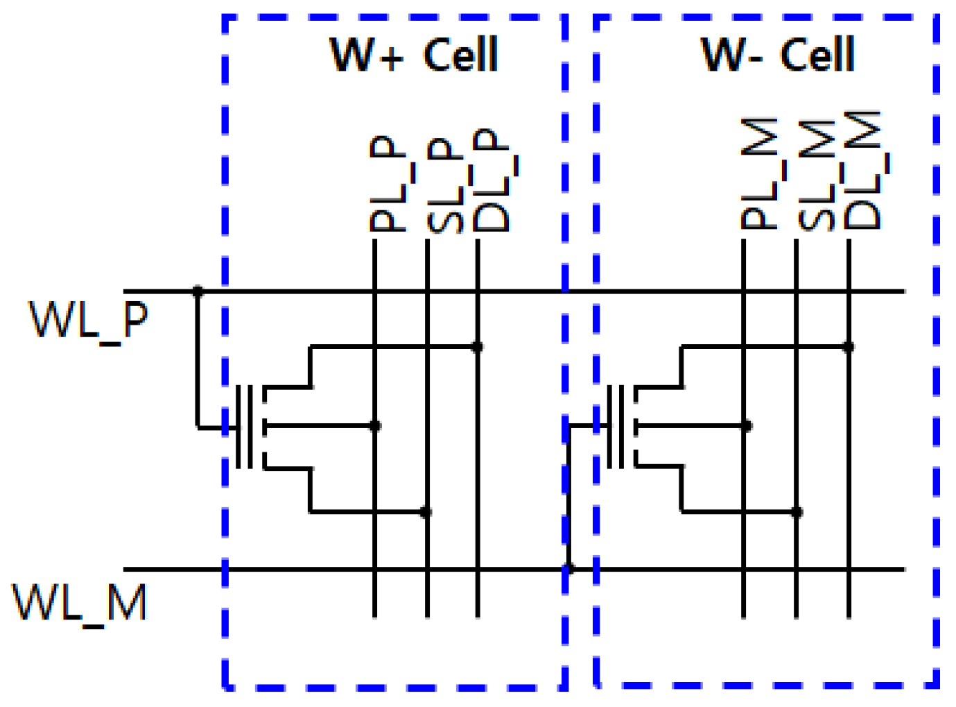
3.1. TFT eFlash-Based Synapse Cell

Figure 2 shows the schematic cross-sectional views of the fabrication steps of the fully CMOS-compatible eFlash synaptic device [26]. After the formation of the p-body, n+ poly-Si is deposited via low-pressure chemical vapor deposition (LPCVD). Through chemical mechanical polishing (CMP) and chemical dry etching (CDE), n+ source/drain (S/D) are identified. Poly-Si is used as a channel material, and a gate insulator stack of Al2O3/Si3N4/SiO2 (A/N/O) is formed. The metal gate of TiN is formed through metal-organic chemical vapor deposition (MOCVD). Finally, after the formation of the passivation layer, metal wires are formed through sputtering.
Table 1 shows the bias conditions for each operation mode of the charge-trapped flash (CTF) type TFT eFlash cell in Figure 2. The erase operation (ERS) of the TFT eFlash cell makes the cell current less than 50 pA in an OFF state and applies to erase voltage (VERS), 0 V, 0 V, and 0 V to the word line (WL), the drain line (DL), source line (SL), and p-poly line (PL), respectively. When VERS is applied with a single pulse of 8 V, electron injection occurs from the bulk of the eFlash cell to the charge-trapping insulator; thus, the erase operation lowers the cell current to 50 pA or less by increasing cell threshold voltage VT. When data is ‘1’ in program mode (PGM), WL, DL, SL, and PL are applied with 0 V, floating, floating, and program voltage (VPGM), respectively, to discharge electrons from the insulator to p-poly so that the cell current has a target current of about 50 nA when the cell is in the ON state. During the program operation, a 1-ms program pulse at 7 V is applied 100 times and a program-verify-read (PVR) operation is performed for each pulse in the synaptic driving circuit. If the eFlash cell current is less than 50 nA, the program operation is continuously performed on the TFT eFlash cell. If the eFlash cell current is more than 50nA, the program pulse is masked using circuitry so that the program operation does not occur in the cell and the cell current is maintained at the target current of 50 nA. When data is ‘0’ in program mode, the erase state is maintained by applying 0 V to both WL and PL. Lastly, in read mode, VRD (=1.5 V) and VDL (=2 V) are applied to the selected WL and DL, while 0 V is applied to SL and PL. With the bias condition, an OFF current (<50 pA) flows from a cell programmed with data ‘0’, whereas an ON current of 50 nA flows from a cell programmed with data ‘1’.
In a binary/ternary weighted NN, synaptic cells that can program weights of +1, −1, and 0 are required. Table 2 shows the functional truth table of the newly proposed synaptic cell with weights of +1, −1, and 0. As shown in Table 2, when the input data and synaptic weight are 1 and +1, respectively, the synapse cell current Icell is IW+ (=50 nA), and when the input data and synaptic weight are 1 and −1, the Icell is -IW-. In the synaptic cell, the W+ cell and W− cell adjust the program current to 50 nA within 1 % error through program-verify-read operation, so the IW+ and IW- current are in the range of 49.5 nA and 50.5 nA. On the other hand, when the input data is 0, The Icell is 0 regardless of the synaptic weight.
Figure 3 shows the circuit of the synapse cell with programmable weights of +1, −1, and 0. Synapse cell performs chip erase operation on the entire chip before program operation. As shown in Table 3, the chip erase operation can be conducted when VERS, 0 V, 0 V, and floating voltage are applied to WL, SL, PL, and DL for both W+ and W− cells, respectively; thus, the TFT eFlash cell current of both W+ and W− cell is less than 50 pA in the OFF state. When the synaptic weight is +1 (−1), the W+ cell (W− cell) is programmed in Figure 3. For programming of the selected W+ cell, the WP_WMb signal is set to ‘1’, and the WL_P, SL_P, PL_P, and DL_P signals are set to 0 V, floating voltage, VPGM, and floating voltage, respectively. During the programming of the selected W+ cell, a program inhibits voltage (VINHP = 4 V) is applied to the WL_P of unselected W+ row cells to prevent programming. For programming the unselected column cell as ‘0’, 0 V instead of VPGM is applied to the PL_P. During the programming of the W+ cell, the WL_M and PL_M signals for the W− cell are set to the VINHP and 0 V voltages to prevent W− cells from programming, respectively. Next, to program the W− cell, the WP_WMb signal is set to ‘0’, and the cell bias condition for programming the W+ cell can be identically applied to the W− cell. To prevent the W+ cell from being programmed, the program inhibit condition is also applied to the W+ cell.
The 324 × 80 synapse cell array circuit of the first layer is shown in Figure 4. Since the operation of two synapse arrays is similar, operations are explained using the first array as an example. Erase mode applies an active high pulse to the erase signal ERS1 and activates the write pulse signal WP1 high for the erase time of 10 ms (Figure 5a). When the erase mode operation is performed, the W+ and W− cells of the 324 × 80 synapse cell array in the first layer are erased simultaneously, and the TFT eFlash cell current drops below 50 pA. After the erase operation, the program data is loaded into the 80-bit page buffer (Figure 5b). Then, the program mode operation is performed (Figure 5c). In program mode, after applying a high pulse to PGM1, a 1-ms WP1 pulse is continuously applied 100 times. In the program mode timing diagram, the READ1 pulse is always applied before the WP1 pulse is activated, and PVR operation is performed in the section where the READ1 pulse is activated as high. In PVR operation, if the read current of the cell to be programmed is less than 50 nA, the next incoming WP1 pulse continues the program operation for the corresponding cell. In contrast, if the TFT eFlash cell current is more than 50 nA, the writing mask (WM) signal becomes high and drives the corresponding PL voltage to 0 V, preventing the corresponding cell from being programmed anymore. Figure 4b shows synapse cells A, B, C, and D programmed into W+, W-, W-, and W− cells, respectively. In the read mode, the READ1 signal is set to high, and then the MSB_EN1 and PWM1[15:0] signals for 8-bit PWM conversion are applied to the synapse array (Figure 5d). All WL_P and WL_M signals are applied with 8-bit PWM pulses in the read mode. Figure 4c shows that when VRD (=1.5 V) is applied to WL_P and WL_M, the current of 50nA (50 nA) and 0 nA (100 nA) flows through IDL_P[1] (IDL_M[1]) and IDL_P[80] (IDL_M[80]), respectively. Synapse cell operation for binary/ternary weighted NN operation is completed by subtracting the DL_M current from the DL_P current in the following neuron circuits.

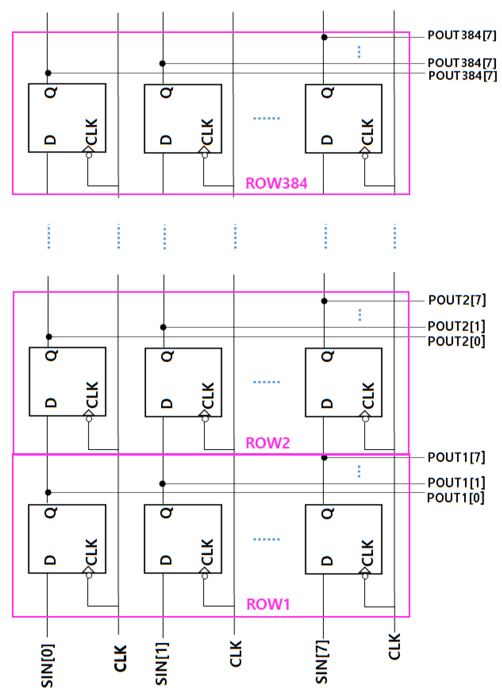
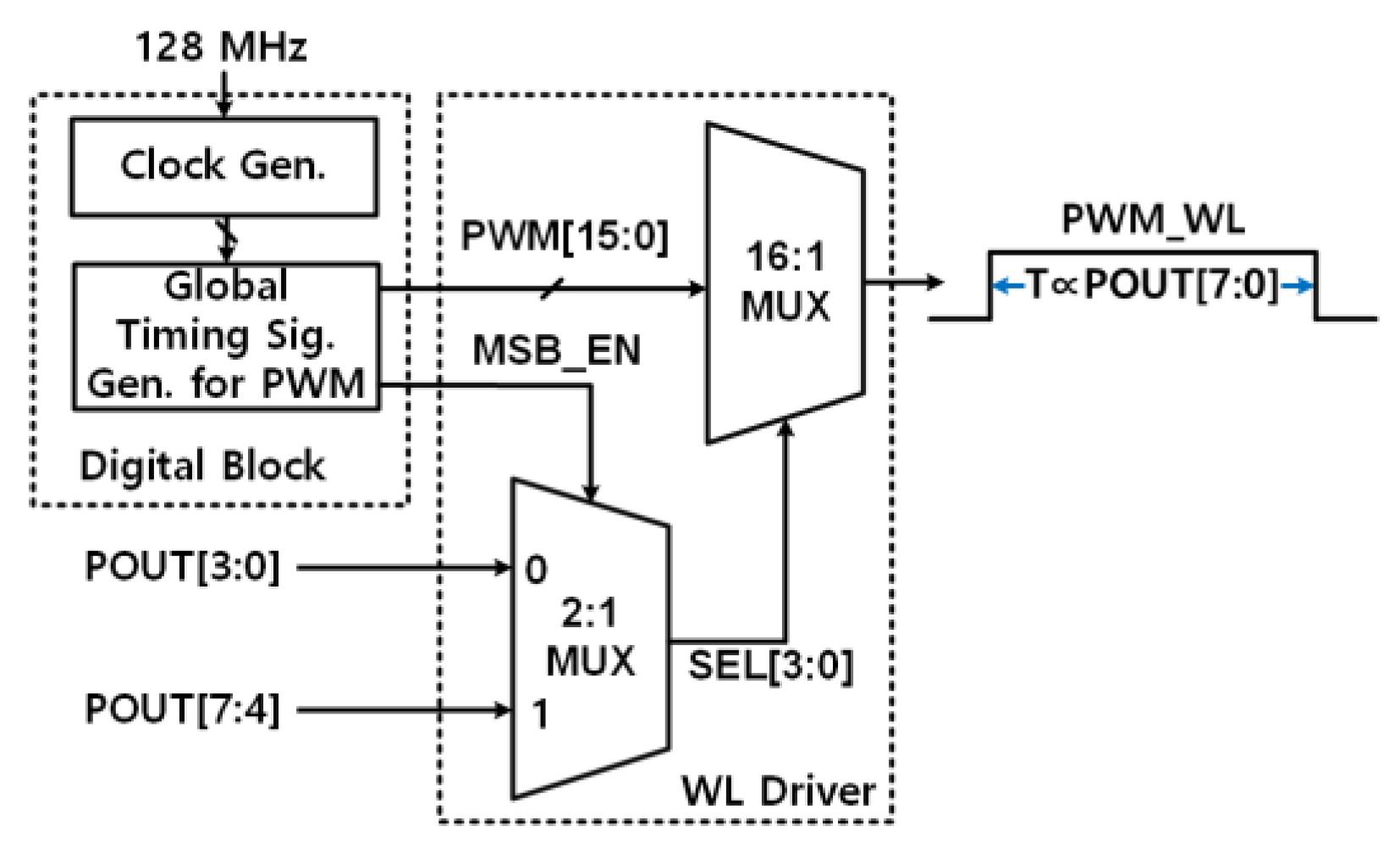
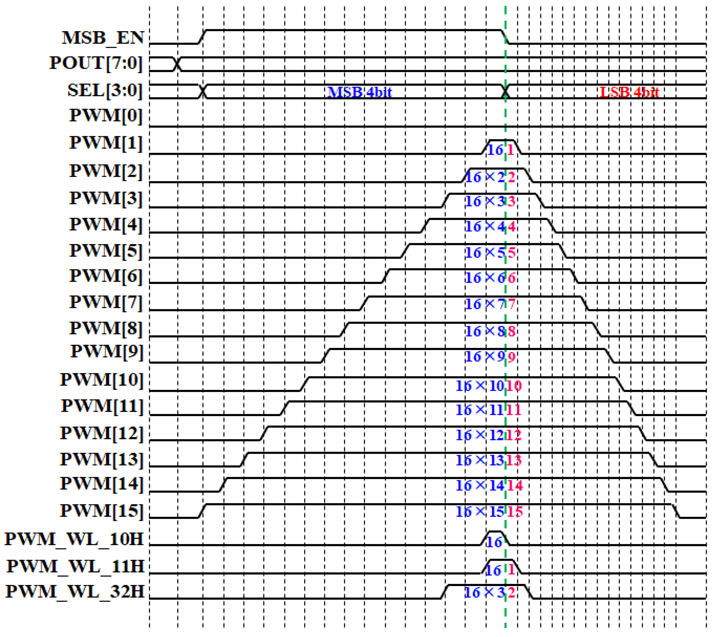
3.2. Pulse Width Modulation Circuit Using Deserializer and Global Signals

The deserializer of the first layer shown in Figure 1 is a circuit for dumping 8-bit data to 324 rows. As shown in Figure 6, the deserializer circuit consists of 324 negative edge-triggered D flip-flops (F/Fs) using an 8-bit data bus in the vertical direction. The serialized input data SIN[7:0] comes in from the bottom, and each serialized input data shifts upward in the vertical direction by one row at the falling edge of the clock signal. After 324 clock cycles, all 8-bit input data are deserialized and connected to the input, POUT[7:0], of the PWM conversion circuit inside the WL driving circuit located on each row.
To convert 8-bit digital input data into time domain information, the PWM conversion circuit can be duplicated for each row. However, when a high frequency is used to obtain an acceptable resolution and the number of rows is large, this structure may increase hardware power consumption and area overhead. In addition, if the converted pulses have multiple edges, linearity may be degraded due to non-idealities caused by multiple Icell charging phases. The PWM conversion method [19] is adopted to solve this problem. It generates a single continuous pulse using global signals PWM[15:0]. The PWM conversion circuit consists of the shared module that generates the global signals (i.e., PWM[k] where 0 ≤ k ≤ 15) for PWM conversion and MUXs (i.e., 2:1 and 16:1 MUX) in each WL driver block (Figure 7). Since a high-frequency clock is used only for one module to generate global signals that are shared by all rows, dynamic power consumption and area overhead can be minimized. Additionally, the 16:1 MUX can be shared due to the two-step conversion process to generate a single pulse for each row, reducing area overhead. The two-step conversion process creates a PWM_WL signal with a pulse width proportional to the input POUT[7:0] as follows:
P W M W L = M S B E N & P W M [ D e c i m a l ( P O U T [ 7 : 4 ] ) ] + M S B E N ¯ & P W M [ D e c i m a l ( P O U T [ 3 : 0 ] ) ] = P O U T [ 7 : 0 ] × t r e f
where tref is the minimum pulse width. Since the value of unsigned four bits can be from 0 to 15, the pulse width of PWM[k] (=tPWM,k) is set as follows with an appropriate delay to output a single pulse.
t P W M , k = ( 16 × k + k ) × t r e f   w h e r e   k ( 0 , 1 , 2 , , 15 )
For example, a two-step conversion process can be illustrated in Figure 8 when POUT[7:0] is hexadecimal 32H. When the MSB_EN signal is ‘1’, 3H is multiplexed as SEL[3:0] in the 2:1 MUX circuit. PWM[3] is then multiplexed in the 16:1 MUX circuit to produce a width of 16 × tref × SEL[3:0] as the PWM_WL signal. When the MSB_EN signal switches from ‘1’ to ‘0’, 2H is multiplexed as SEL[3:0] in the 2:1 MUX circuit. PWM[2] is multiplexed in the 16:1 MUX circuit to produce a width of tref × SEL[3:0] as the PWM_WL signal. Therefore, a single pulse PWM_WL signal having the total width of tref × POUT[7:0] is finally output.

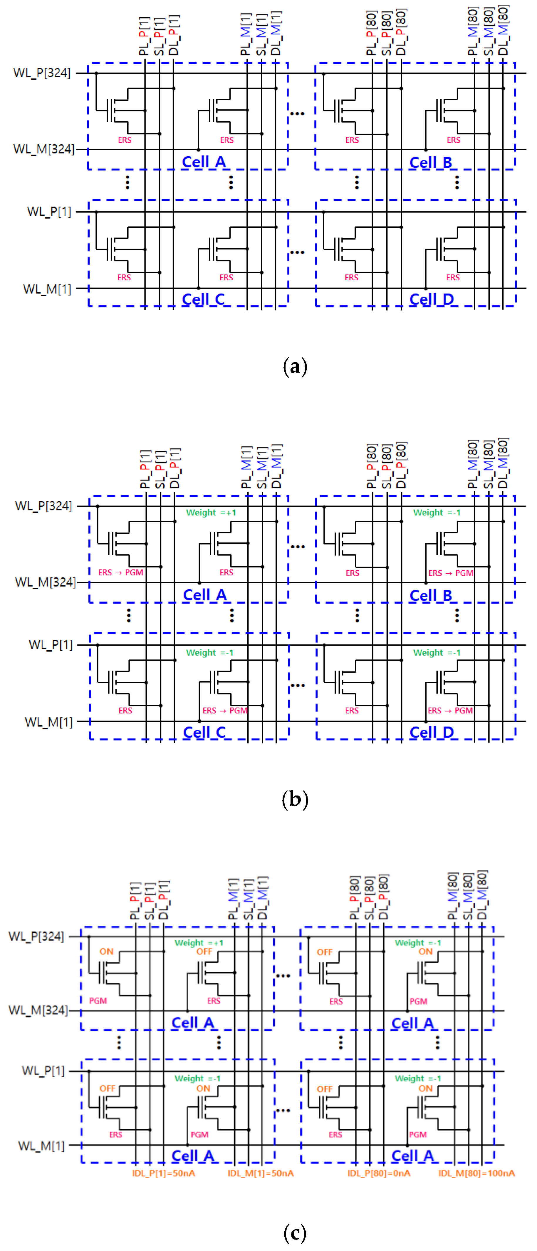
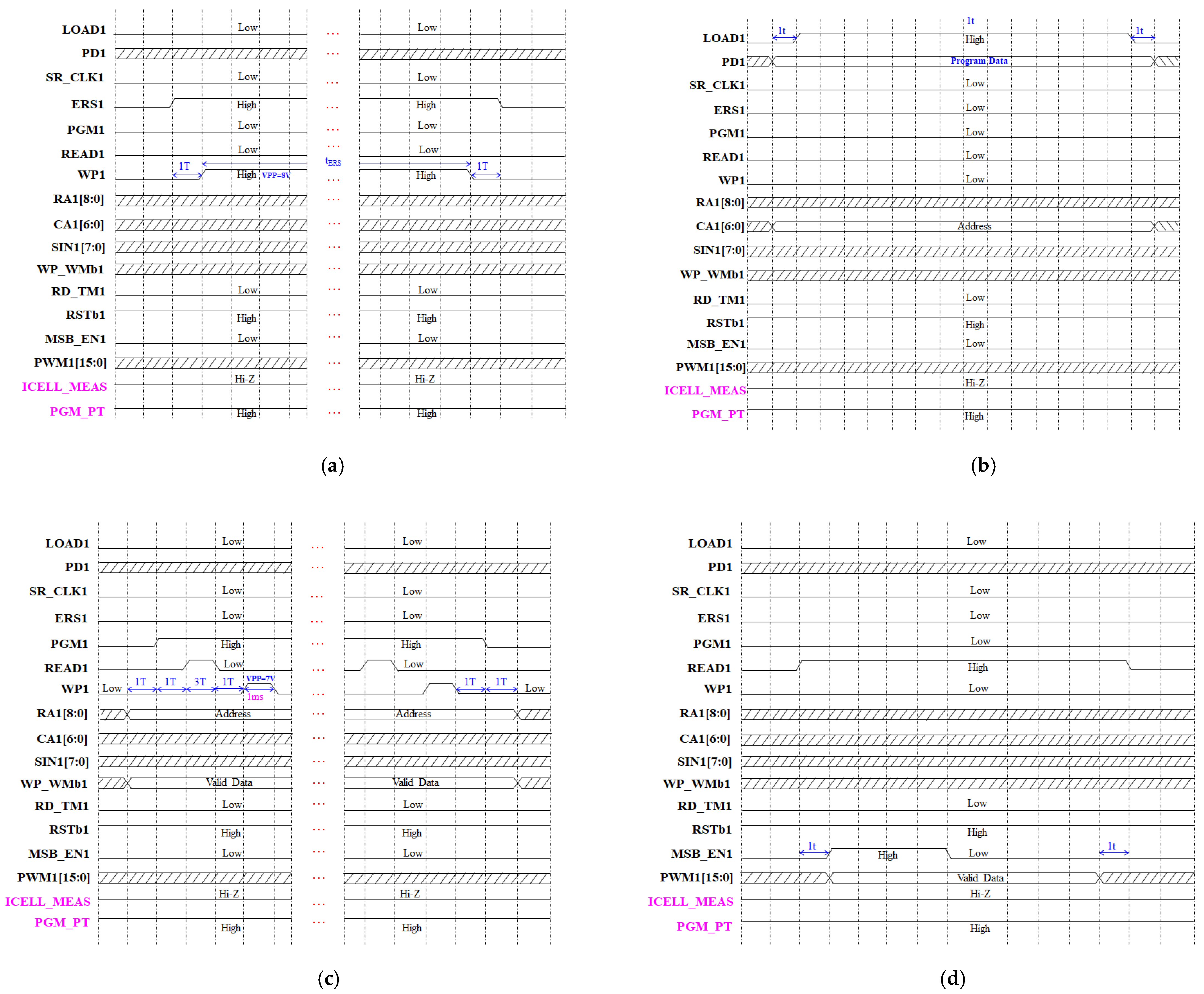
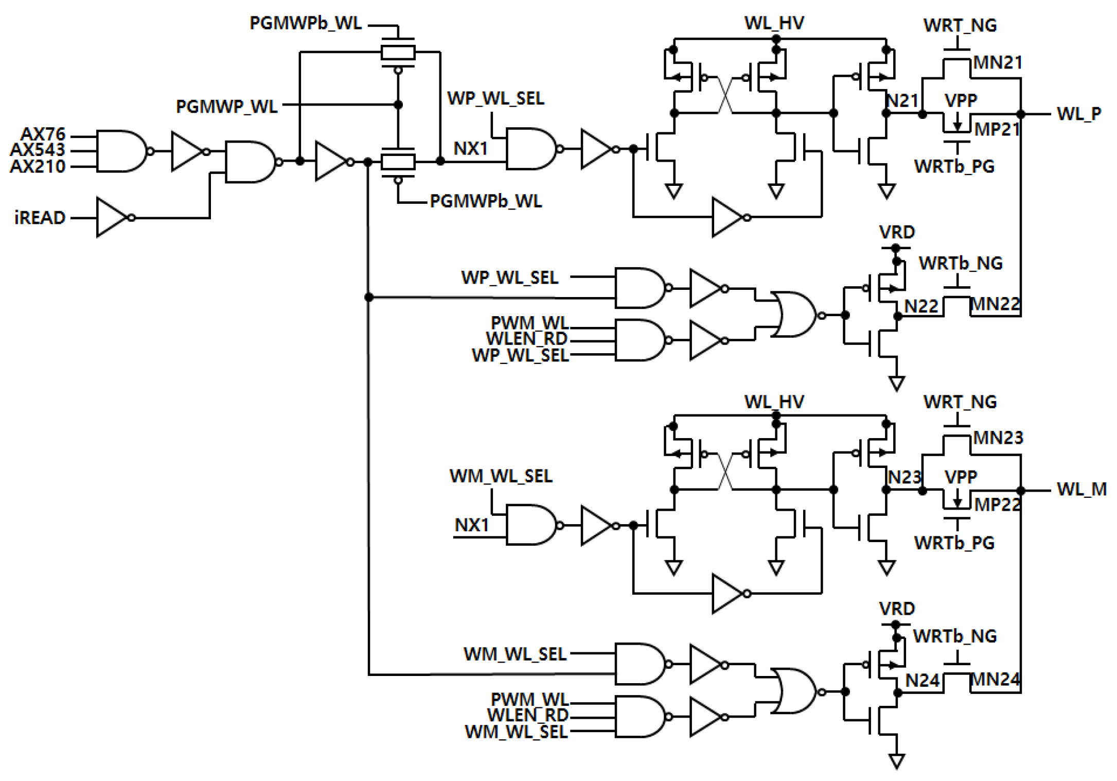
3.3. Synaptic Driving Circuit

The proposed synaptic driving circuit has six modes, as shown in Table 4. The page buffer load mode uploads the data to be programmed to the page buffer before programming, and the shift register load mode loads 8-bit input data for each row through the shift operation. The test read mode is used to test the read current of the TFT eFlash cell after erasing or programming each W+ and W− cell in the synapse array. The WL and PL drivers of the synaptic driving circuits require switching power supply voltages (i.e., WL_HV and PL_HV voltages, respectively) that are changed for each operation mode. WL_HV is set to VERS (=8 V) for 10 ms in the chip erase mode and VINH (=4 V) in other operation modes. The WL_PL voltage is set to VPGM (=7 V) with the pulse train where the 1-ms pulse width is repeated 100 times in program mode and VDD in other operation modes.
Figure 9 shows the WL_HV and PL_HV switching circuits for the power supply of the WL and PL driver, respectively. In the WL_HV switching circuit (Figure 9a), VPP_SEL (VPP_SELb) signal is set to VPP (0 V) in erase mode; thus, WL_HV switching circuit outputs VPP (=VERS) voltage. On the other hand, in non-erase mode, the VPP_SEL (VPP_SELb) signal is set to 0 V (VPP); thus, WL_HV switching circuit outputs VINH. MP3 and MP4 (MP5 and MP6) are transistors that connect the higher voltage between VPP and WL_HV (WL_HV and VINH) to the N1 (N2) node. The PL_HV switching circuit in Figure 9b outputs VPP (=VPGM) voltage through MP11 in program mode, and it outputs VDD through MP12 in other operation modes.
The WL driving circuit using WL_HV switching power is shown in Figure 10. Since WRT_NG, WRTb_PG, and WRTb_NG signals are set to 0 V, WL_HV, and 0 V in erase or program mode (Table 4), respectively, the voltage of nodes N21 (N23) is transferred to WL_P (WL_M). In non-erase or non-program mode, WRT_NG, WRTb_PG, and WRTb_NG signals are set to WL_HV, 0 V, and VDD voltages, respectively, so the voltage of nodes N22 (N24) is transferred to WL_P (WL_M). Therefore, the voltages of WL_P and WL_M satisfy the cell bias conditions in the erase and program mode of Table 3 and the conditions in the test read and read mode of Table 5.
The PL driving circuit using the PL_HV switching power is shown in Figure 11a. Suppose the program data is ‘1’ in program mode (Table 3 and Table 5). When the WP_WMb signal is ‘1’ and the read current of the selected W+ cell is less than 50 nA, the PL_P signal outputs VPGM. On the other hand, when WP_WMb signal is ‘0’ and the read current of the W− cell is less than 50 nA, the PL_M signal outputs VPGM to continue programming the cell. In all other cases, the PL_P and PL_M signals are driven to 0 V. The SL driving circuit is shown in Figure 11b. In program mode, MN31 and MN32 are turned off, so SL_P and SL_M of all columns are floating. Additionally, the MN31 and MN32 transistors are turned on to drive the SL_P and SL_M signals to 0 V.
Figure 12 shows the current comparator circuit that compares whether the selected TFT eFlash cell is programmed with 50 nA or not when program data is ‘1’ in program mode. In the read mode, the current comparator circuit transfers the Icell of W+ or W− cell to the PMOS cascode current mirror (MP41, MP42, MP43, and MP44) through the DL_P line or DL_M line controlled by the WP_DL_SEL and WM_DL_SEL signals, respectively. Since the cascode current mirror ratio is 1:2, the output current is 2·Icell. If this 2·Icell current is smaller (larger) than the reference current Iref (=100 nA), the iCELL_PGMb signal outputs ‘1’ (‘0’). When the iCELL_PGMb signal changes from ‘1’ to ‘0’ while performing the PVR function in program mode, the TFT eFlash cell current is programmed with more than the target current (=50 nA) because the 2·Icell current is more than 100 nA. When performing the PVR function, the proposed current sensing circuit maintains the N41 (N44) node voltage at VREF_VDL (=2 V) using negative feedback with the opamp, DIFF41 (DIFF42), and MN43 (MN44). By maintaining the cascode current mirror’s output voltage as VREF_VDL voltage, the current variation by channel length modulation can be minimized in the cascode current mirror.

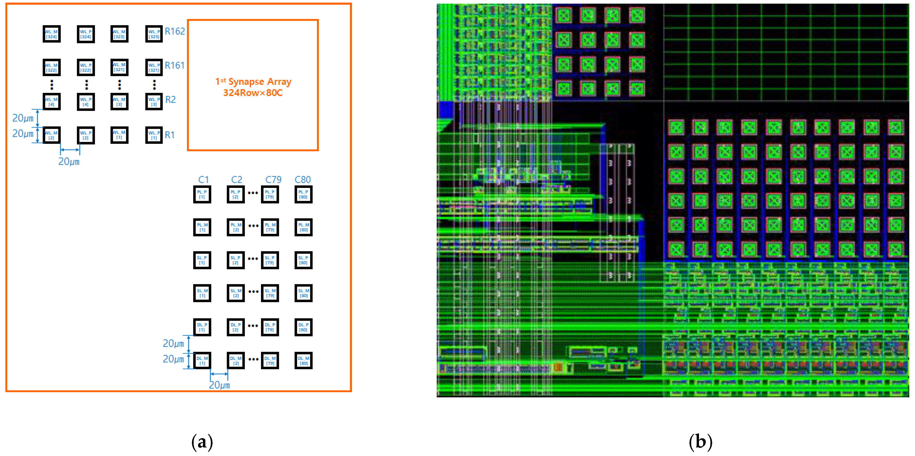
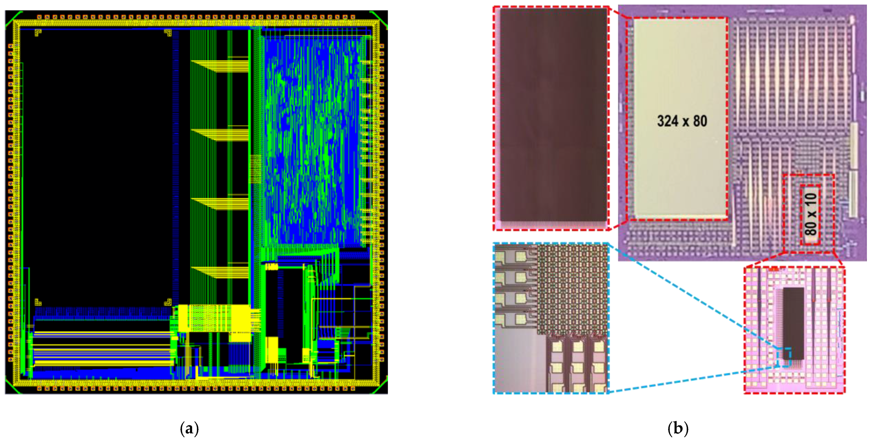
4. Chip Packing Using Hybrid Bonding Technology

In commercial foundry service FAB, merging the TFT eFlash process with the CMOS process is challenging due to the high-temperature process. Therefore, hybrid bonding technology is proposed for packaging the proposed synaptic driving circuit die and the TFT eFlash-based synapse array die (Figure 13). It consists of (1) bump bonding of a 0.35 μm CMOS die and a TFT eFlash die and (2) wire bonding with the 0.35 μm CMOS die on the PCB substrate. When WL driver-related bump bonding pad is placed in each row, the 324-row layout length impractically increases to 12,960 μm because the bump bonding pad pitch is 40 μm. The row pitch size of the first layer can be reduced by half by placing the four bump bonding pads of two row-related signals (i.e., two WL_P and two WL_M) parallel in one row (Figure 14). The proposed accelerator with a network size of 324 × 80 × 10 is designed with a 9 mm × 9 mm layout size using a standard 0.35 μm CMOS process, and two eFlash-based synapse arrays are fabricated using conventional CMOS technology (Figure 15).

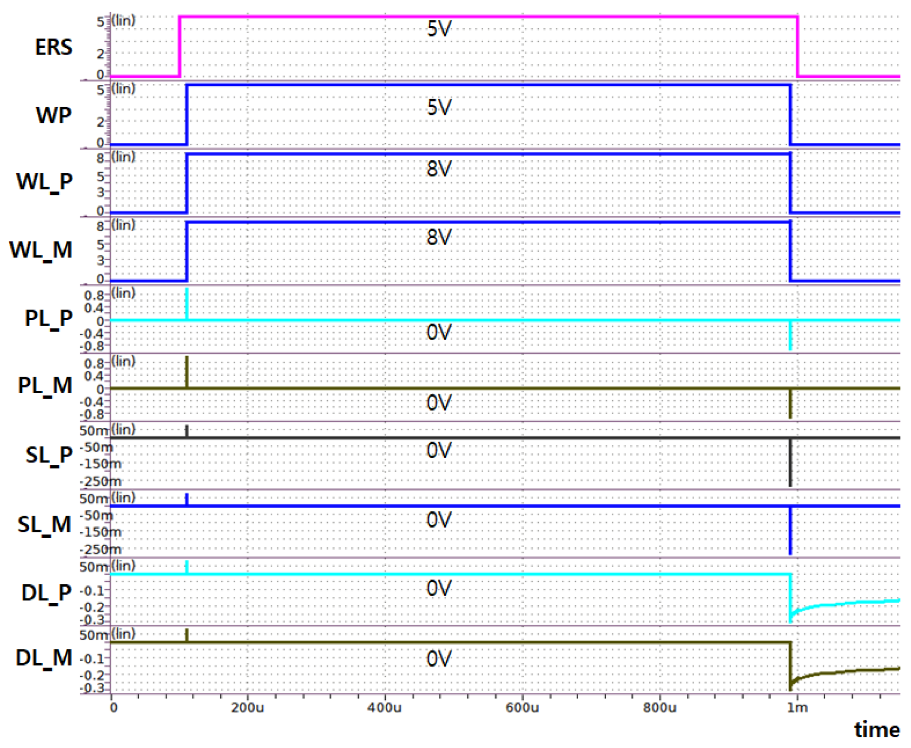
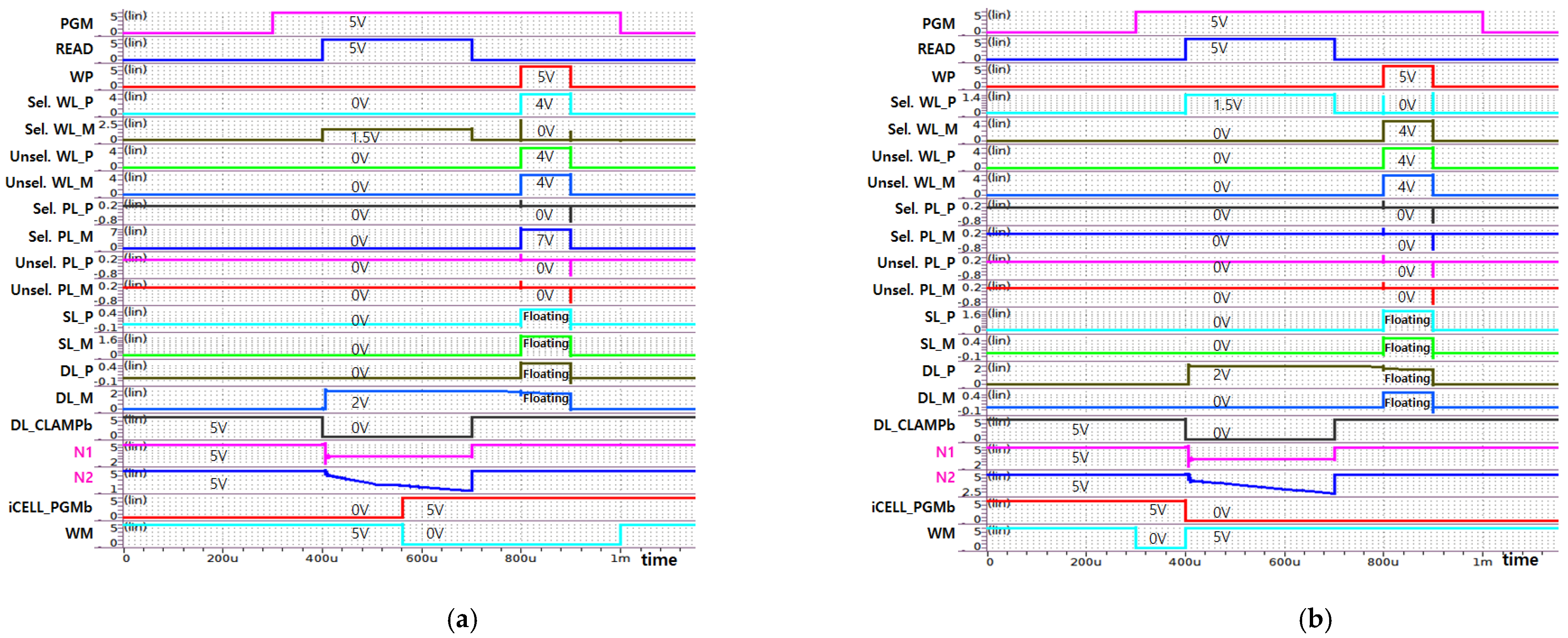
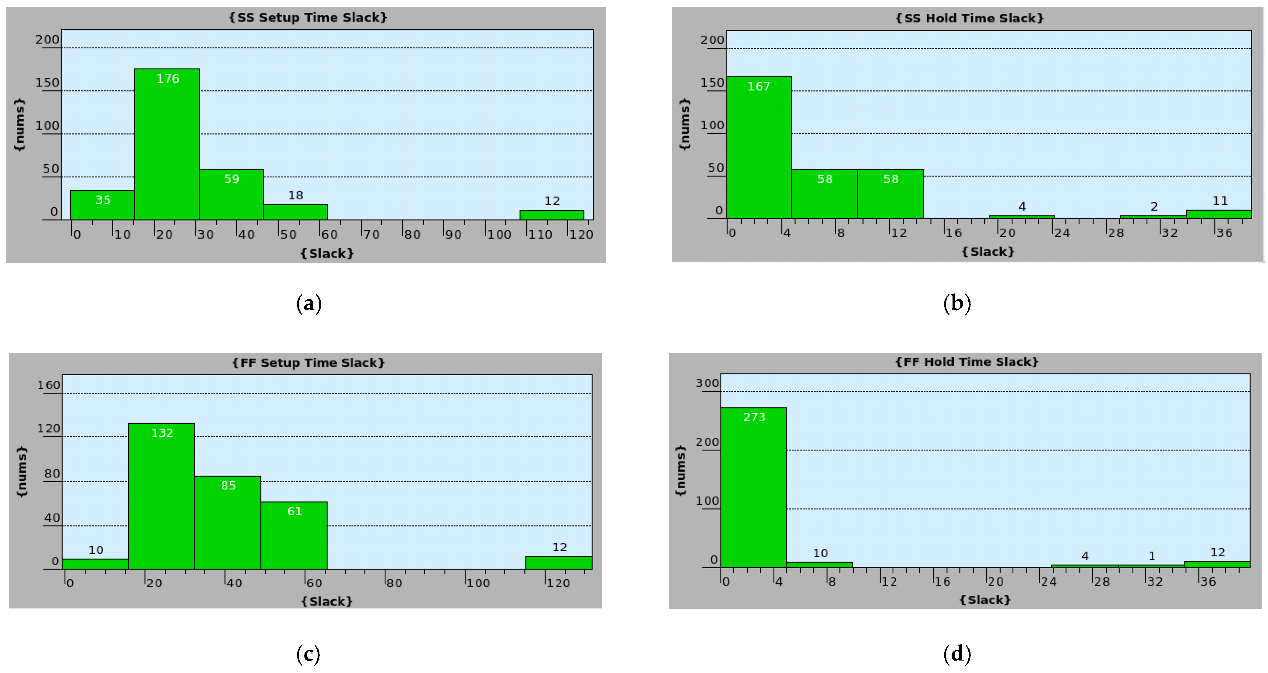
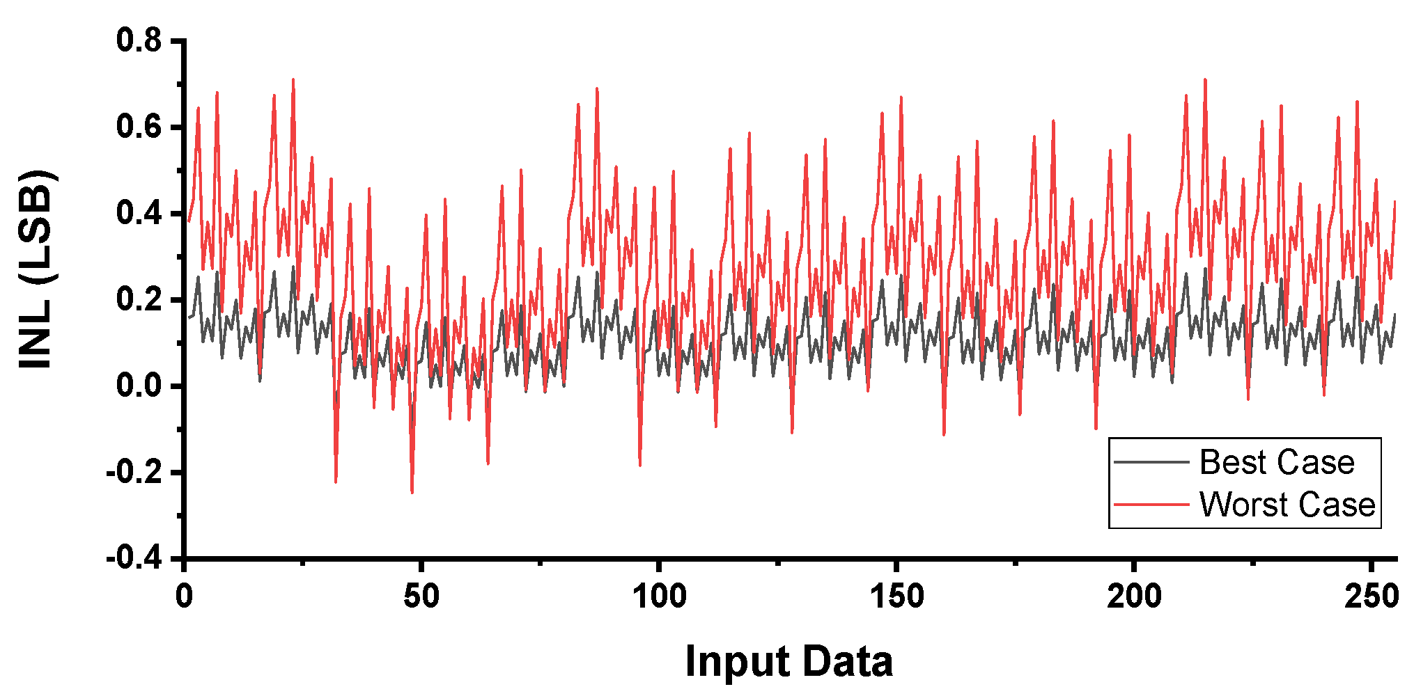
5. Simulation Results

For circuit verification, a simulation was performed using Synopsys Hspice. Figure 16 shows the simulation result for the erase mode under the conditions of VDD = 5 V, TT model parameter, and temp. = 25 °C for the first-layer synapse array IP of the proposed system designed using the 0.35 μm CMOS process. When the ERS signal is applied, the gate voltage of the cell (WL_P and WL_M) is set to the VERS (=8 V) voltage. Additionally, the p-poly line (PL_P and PL_M) and source (SL_P and SL_M) are set to 0 V. Since W+ and W− cells are turned on by VERS, drain (DL_P and DL_M) are biased to the source voltage. All cells’ data in each synapse array are erased under the bias condition in Table 3.
Figure 17 shows simulation results for the program mode under the conditions of VDD = 5 V, TT model parameter, temp. = 25 °C. When the PGM signal is applied, the PVR function is performed by the READ signal. In the case of 49-nA Icell with iCELL_PGMb = ‘1’, the corresponding eFlash cell is treated as an unprogrammed cell because Icell does not reach the target current (=50 nA ± 0.5 nA). So, the cell continues to be programmed by the WP (Write Program) signal. In contrast, in the case of 49.5-nA Icell with iCELL_PGMb = ‘0’, the program operation of the cell is performed because Icell satisfies the target current. The selected cell is no longer programmed when the WM (Write Mask) signal is ‘1’. Therefore, the proposed circuit can accurately program the Icell with the target current using the current comparator in Figure 13.
Figure 18 shows the read simulation result with the parasitic extraction when the shift register of 324 rows is loaded with hexadecimal FFH in the synaptic driving circuit of the first synapse array where all W+ (W-) cells are programmed as ‘1’ (‘0’). To generate Io in (1), the gate (WL_P and WL_M) is biased to 1.5 V during the modulated pulse width of FFH (i.e., tref × 15 × (16 + 1)). As a result of the read operation, Io (i.e., DL_P current - DL_M current) is reduced from 16.2 μA (=Icell × 324) to 14.8 μA by IR drop due to the parasitic resistance.
When compared with memory cells in previous works, the proposed TFT eFlash cell can be programmed at 50 nA, reducing the power consumption in current-mode PIM operation (Table 6).
For digital circuit implementation, synthesis and auto PnR are performed using Synopsys Design Compiler and IC Compiler, respectively. To validate the timing performance, post-layout static timing analysis is then performed in the best (FF corner, 5.5 V, 0 °C) and worst (SS corner, 4.5 V, 125 °C) cases using Synopsys PrimeTime. Digital blocks include a serializer for the off-chip interface, an eFlash write/read control block, a row/column decoder, a multi-clock generator, a system control block, and a global timing signal generator for PWM. When the maximum frequency of 64 MHz is applied, the minimum timing margin is 0.51 ns for setup in the worst case and 0.14 ns for hold in the best case (Figure 19). Power consumption of the synthesized digital blocks is estimated to be 19.5 mW (31.6 mW) in the worst (best) corner using Synopsys PrimeTime after auto PnR.
Post-layout simulation is performed to derive DC performance of the PWM conversion circuit. Since the 4-phase 32-MHz (i.e., effective 128-MHz) clock is used for PWM to achieve the maximum width of less than 2 μs, the ideal value for tref is 7.815 ns (=1 LSB). The integral nonlinearity error (INL) is [−0.11 LSB, 028 LSB] and [−0.25 LSB, 0.71 LSB] in the best and worst cases, respectively, as shown in Figure 20.

6. Conclusions

A TFT eFlash memory-based PIM hardware for edge computing is designed and laid out using a 0.3 μm CMOS process. The prototype chip includes 324 × 80 × 10 synapse arrays composed of the eFlash-based binary/ternary weighted synaptic cells that can be programmed with negative weight values.
The proposed synaptic driving circuit uses a high voltage switching power circuit to perform erase and program operations of the synaptic array. To improve the operation accuracy of PIM during the read operation, the proposed circuit precisely programs the sensing current of the eFlash cell to a target current of 50 nA ± 0.5 nA using a program pulse train. In addition, a global signal-based PWM conversion circuit is used to improve linearity in the synaptic sensing current integration step of the neuron circuit by converting 8-bit input data into one continuous pulse.
Finally, hybrid bonding technology is used to (1) connect the two dies by bump bonding and (2) connect the die and the PCB by wire bonding. When applied, two separately manufactured dies can be combined into a single package. It is expected to be applied to the design of non-volatile memory-based accelerator chips (e.g., large-capacity NAND eFlash).

Author Contributions

Conceptualization, Y.K., C.L., J.L. and H.S.; methodology, Y.K., C.L., J.L. and H.S.; validation, H.J., D.K., M.-K.P., J.H., J.-M.W. and J.C.; formal analysis, H.S.; writing—original draft preparation, Y.K., P.H. and H.S.; writing—review and editing, Y.K. and H.S.; visualization, H.J., D.K., M.-K.P., J.H. and J.-M.W.; project administration, J.Y.K. All authors have read and agreed to the published version of the manuscript.

Funding

This work was supported by the Institute of Information & communications Technology Planning & Evaluation (IITP) grant funded by the Korean government (MSIT) (2021-01-01776, Development of PIM synaptic array and artificial neural network hardware based on eFLASH memory).

Acknowledgments

The EDA tool was supported by the IC Design Education Center (IDEC), Republic of Korea.

Conflicts of Interest

The authors declare no conflict of interest.

References

  1. Krizhevsky, A.; Sutskever, I.; Hinton, G.E. ImageNet Classification with Deep Convolutional Neural Networks. In Proceedings of the Neural Information Processing Systems (NIPS), Lake Tahoe, NV, USA, 3–8 December 2012. [Google Scholar]
  2. Simonyan, K.; Zisserman, A. Very Deep Convolutional Networks for Large-Scale Image Recognition. In Proceedings of the International Conference on Learning Representations (ICLR), Ottawa, ON, Canada, 10–13 June 2015. [Google Scholar]
  3. He, K.; Zhang, X.; Ren, S.; Sun, J. Deep Residual Learning for Image Recognition. In Proceedings of the IEEE Computer Vision and Pattern Recognition Conference (CVPR), Las Vegas, NV, USA, 26 June–1 July 2016. [Google Scholar]
  4. Szegedy, C.; Ioffe, S.; Vanhoucke, V.; Alemi, A. Inception-v4, Inception-ResNet and the Impact of Residual Connections on Learning. In Proceedings of the Thirty-First AAAI Conference on Artificial Intelligence, San Francisco, CA, USA, 4–9 February 2017. [Google Scholar]
  5. Tan, M.; Le, Q.V. EfficientNet: Rethinking Model Scaling for Convolutional Neural Networks. In Proceedings of the Machine Learning Research, Long Beach, CA, USA, 9–15 June 2019. [Google Scholar]
  6. Hubara, I.; Courbariaux, M.; Soudry, D.; El-Yaniv, R.; Bengio, Y. Binarized Neural Networks. In Proceedings of the Neural Information Processing Systems (NIPS), Barcelona, Spain, 5–10 December 2016. [Google Scholar]
  7. Rastegari, M.; Ordonez, V.; Redmon, J.; Farhadi, A. XNOR-Net: ImageNet Classification Using Binary Convolutional Neural Networks. In Proceedings of the European Conference on Computer Vision (ECCV), Amsterdam, The Netherlands, 8–16 October 2016. [Google Scholar]
  8. Kim, M.; Smaragdis, P. Bitwise Neural Networks. In Proceedings of the International Conference on Learning Representations (ICLR), San Diego, CA, USA, 7–9 May 2015. [Google Scholar]
  9. Iandola, F.N.; Han, S.; Moskewicz, M.W.; Ashraf, K.; Dally, W.J.; Keutzer, K. SqueezeNet: AlexNet-level accuracy with 50× fewer parameters and <0.5 MB model size. arXiv 2016, arXiv:1602.07360. [Google Scholar]
  10. Huang, G.; Liu, Z.; van der Maaten, L.; Weinberger, K.Q. Densely Connected Convolutional Networks. In Proceedings of the IEEE Computer Vision and Pattern Recognition Conference (CVPR), Honolulu, HI, USA, 22–25 July 2017. [Google Scholar]
  11. Howard, A.G.; Zhu, M.; Chen, B.; Kalenichenko, D.; Wang, W.; Weyand, T.; Andreetto, M.; Adam, H. MobileNets: Efficient Convolutional Neural Networks for Mobile Vision Applications. arXiv 2017, arXiv:1704.04861. [Google Scholar]
  12. Zhang, X.; Zhou, X.; Lin, M.; Sun, J. Shufflenet: An extremely efficient convolutional neural network for mobile devices. In Proceedings of the IEEE Conf. Comput. Vis. Pattern Recognit. (CVPR), Salt Lake City, UT, USA, 19–21 June 2018. [Google Scholar]
  13. Horowitz, M. 1.1 Computing’s Energy Problem (and what we can do about it). In Proceedings of the IEEE International Solid-State Circuits Conference (ISSCC), San Francisco, CA, USA, 9–13 February 2014. [Google Scholar]
  14. Chen, Y.-H.H.; Krishna, T.; Emer, J.S.; Sze, V. Eyeriss: An Energy-Efficient Reconfigurable Accelerator for Deep Convolutional Neural Networks. IEEE J. Solid-State Circuits 2017, 52, 127–138. [Google Scholar] [CrossRef] [Green Version]
  15. Moons, B.; Verhelst, M. An Energy-Efficient Precision-Scalable ConvNet Processor in 40-Nm CMOS. IEEE J. Solid-State Circuits 2017, 52, 903–914. [Google Scholar] [CrossRef]
  16. Whatmough, P.N.; Lee, S.K.; Lee, H.; Rama, S.; Brooks, D.; Wei, G. 14.3 A 28nm SoC with a 1.2GHz 568nJ/Prediction Sparse Deep-Neural-Network Engine with >0.1 Timing Error Rate Tolerance for IoT Applications. In Proceedings of the IEEE International Solid-State Circuits Conference (ISSCC), San Francisco, CA, USA, 5–9 February 2017. [Google Scholar]
  17. Sze, V.; Chen, Y.-H.; Yang, T.-J.; Emer, J.S. Efficient Processing of Deep Neural Networks: A Tutorial and Survey. Proc. IEEE 2017, 105, 2295–2329. [Google Scholar] [CrossRef] [Green Version]
  18. Kang, M.; Gonugondla, S.K.; Patil, A.; Shanbhag, N.R. A Multi-Functional In-Memory Inference Processor Using a Standard 6T SRAM Array. IEEE J. Solid-State Circuits 2018, 53, 642–655. [Google Scholar] [CrossRef]
  19. Biswas, A.; Chandrakasan, A.P. CONV-SRAM: An Energy-Efficient SRAM With In-Memory Dot-Product Computation Neural Networks. IEEE J. Solid-State Circuits 2019, 54, 217–230. [Google Scholar] [CrossRef] [Green Version]
  20. Son, H.; Cho, H.; Lee, J.; Bae, S.; Kim, B.; Park, H.-J.; Sim, J.-Y. A Multilayer-Learning Current-Mode Neuromorphic System with Analog-Error Compensation. IEEE Trans. Biomed. Circuits Syst. 2019, 13, 986–998. [Google Scholar] [CrossRef] [PubMed]
  21. Bankman, D.; Yang, L.; Moons, B.; Verhelst, M.; Murmann, B. An Always-On 3.8 ΜJ/86% CIFAR-10 Mixed-Signal Binary CNN Processor With All Memory on Chip in 28-Nm CMOS. IEEE J. Solid-State Circuits 2019, 54, 158–172. [Google Scholar] [CrossRef]
  22. Dong, Q.; Sinangil, M.E.; Erbagci, B.; Sun, D.; Khwa, W.; Liao, H.; Wang, Y.; Chang, J. A 351TOPS/W and 372.4GOPS Compute-in-Memory SRAM Macro in 7 nm FinFET CMOS for Machine-Learning Applications. In Proceedings of the IEEE International Solid-State Circuits Conference (ISSCC), San Francisco, CA, USA, 16–20 February 2020. [Google Scholar]
  23. Wang, L.; Ye, W.; Dou, C.; Si, X.; Xu, X.; Liu, J.; Shang, D.; Gao, J.; Zhang, F.; Liu, Y.; et al. Efficient and Robust Nonvolatile Computing-In-Memory Based on Voltage Division in 2T2R RRAM With Input-Dependent Sensing Control. IEEE Trans. Circuits Syst. II 2021, 68, 1640–1644. [Google Scholar] [CrossRef]
  24. Yoon, J.-H.; Chang, M.; Khwa, W.-S.; Chih, Y.-D.; Chang, M.-F.; Raychowdhury, A. A 40-Nm 118.44-TOPS/W Voltage-Sensing Compute-in-Memory RRAM Macro With Write Verification and Multi-Bit Encoding. IEEE J. Solid-State Circuits 2022, 57, 845–857. [Google Scholar] [CrossRef]
  25. Murali, G.; Sun, X.; Yu, S.; Lim, S.K. Heterogeneous mixed-signal monolithic 3-D in-memory computing using resistive RAM. IEEE Trans. Very Large Scale Integr. VLSI Syst. 2020, 29, 386–396. [Google Scholar] [CrossRef]
  26. Kang, W.-M.; Kwon, D.; Woo, S.Y.; Lee, S.; Yoo, H.; Kim, J.; Park, B.-G.; Lee, J.-H. Hardware-Based Spiking Neural Network Using a TFT-Type AND Flash Memory Array Architecture Based on Direct Feedback Alignment. IEEE Access 2021, 9, 73121–73132. [Google Scholar] [CrossRef]
  27. McPartland, R.J.; Singh, R. 1.25 volt, low cost, embedded flash memory for low density applications. In Proceedings of the Symposium on VLSI Circuits, Honolulu, HI, USA, 15–17 June 2000. [Google Scholar]
  28. Song, S.H.; Chun, K.C.; Kim, C.H. A logic-compatible embedded flash memory for zero-standby power system-on-chips featuring a multi-story high voltage switch and a selective refresh scheme. IEEE J. Solid-State Circuits 2013, 48, 1302–1314. [Google Scholar] [CrossRef]
Figure 1. Block diagram of the proposed neural network accelerator with eFlash synapse array.
Electronics 12 00678 g001
Figure 2. Schematic process cross-section of an eFlash cell fully compatible with CMOS process: (a) p-body formation via LPCVD and implantation; (b) n+ poly-Si deposition via LPCVD; (c) CMP & CDE; (d) poly-Si channel formation; (e) gate insulator stack formation; (f) metal gate via MOCVD & inter layer dielectrics (ILD).
Electronics 12 00678 g002
Figure 3. Synaptic cell based on TFT eFlash cell with programmable weights +1, −1, and 0.
Electronics 12 00678 g003
Figure 4. Erase, program and read operations in the 324 × 80 synapse array: (a) erase operation; (b) program operation; (c) read operation.
Electronics 12 00678 g004
Figure 5. Timing diagram for erase, page buffer data load, program and read mode for the synapse driving circuit: (a) erase mode; (b) page buffer data load; (c) program mode; (d) read mode.
Electronics 12 00678 g005
Figure 6. Deserializer circuit used in the first layer.
Electronics 12 00678 g006
Figure 7. PWM conversion circuit.
Electronics 12 00678 g007
Figure 8. Timing diagram for a two-step PWM conversion.
Electronics 12 00678 g008
Figure 9. HV switching circuit used in synaptic core circuit: (a) WL_HV switching circuit; (b) PL_HV switching circuit.
Electronics 12 00678 g009
Figure 10. WL driving circuit in the first layer.
Electronics 12 00678 g010
Figure 11. (a) PL driving circuit; (b) SL driving circuit.
Electronics 12 00678 g011
Figure 12. Current sensing circuit.
Electronics 12 00678 g012
Figure 13. Hybrid bonding technology.
Electronics 12 00678 g013
Figure 14. Bump bonding for the first layer: (a) pad array diagram; (b) layout image.
Electronics 12 00678 g014
Figure 15. (a) Layout of the proposed accelerator chip designed using 0.35 μm CMOS process, and (b) fabricated eFlash-based synapse arrays using conventional CMOS technology.
Electronics 12 00678 g015
Figure 16. Simulation result for the erase mode.
Electronics 12 00678 g016
Figure 17. Simulation results for the program mode according to eFlash cell currents: (a) Icell = 49 nA; (b) Icell = 49.5 nA.
Electronics 12 00678 g017
Figure 18. Post-layout simulation result of read operation when the shift register of 324 rows is loaded with hexadecimal FF.
Electronics 12 00678 g018
Figure 19. Post-layout static timing analysis (STA): (a) setup time slack of the worst case; (b) hold time slack of the worst case; (c) setup time slack of the best case; (d) hold time slack of the best case.
Electronics 12 00678 g019
Figure 20. Simulated INL plot of best and worst case after auto PnR.
Electronics 12 00678 g020
Table 1. Bias conditions of TFT eFlash cell for each operation mode.
OperationNodeWLDLSLPL
ERSChip EraseVERS0 V0 V0 V
PGMSel. WL & Sel. DL/SL0 VFloatingFloatingVPGM
Sel. WL & Unsel. DL/SL0 VFloatingFloating0 V
Unsel. WL & Sel. DL/SLVINHPFloatingFloatingVPGM
Unsel. WL & Unsel. DL/SLVINHPFloatingFloating0 V
ReadSel. WL & Sel. DL/SLVRDVDL0 V0 V
Unsel. WL & Sel. DL/SL0 VVDL0 V0 V
Table 2. Functional truth table of synaptic cells with weights of +1, −1, and 0.
InputSynaptic WeightIcell
1+1IW+
1−1−IW−
100
0+10
0−10
000
Table 3. Bias conditions of TFT eFlash cell for each operation mode.
FunctionWP_WMbSynapse CellWL_PSL_PPL_PDL_PWL_MSL_MPL_MDL_M
Program Mode1Sel. Row & Sel. Col0 VFloatingVPGMFloatingVINHPFloating0 VFloating
Sel. Row & Unsel. Col0 V
Unsel. Row & Sel. ColVINHPVPGM
Unsel. Row & Unsel. Col0 V
0Sel. Row & Sel. ColVINHPFloating0 VFloating0 VFloatingVPGMFloating
Sel. Row & Unsel. Col0 V
Unsel. Row & Sel. ColVINHPVPGM
Unsel. Row & Unsel. Col0 V
Erase ModeXChip EraseVERS0 V0 VFloatingVERS0 V0 VFloating
Table 4. Output voltages of HV switching circuit for each operation mode.
Operating ModeWL_HVPL_HVWRTb_PGWRT_NGWRTb_NG
Chip EraseVERSVDD0 VWL_HV0 V
Page Buffer LoadVINHVDDWL_HV0 VVDD
ProgramVINHVPGM0 VWL_HV0 V
Shift Register LoadVINHVDDWL_HV0 VVDD
ReadVINHVDDWL_HV0 VVDD
Test ReadVINHVDDWL_HV0 VVDD
Table 5. Cell bias conditions for ‘TEST read’ and ‘read’ mode in the proposed synaptic cell.
FunctionWP_WMbSynapse CellWL_PSL_PPL_PDL_PWL_MSL_MPL_MDL_M
TEST
Read Mode
1Sel. Row & Sel. ColVREAD0 V0 VVDD0 V0 V0 VVDD
Sel. Row & Unsel. ColFloatingFloating
Unsel. Row & Sel. Col0 VVDDVDD
Unsel. Row & Unsel. ColFloatingFloating
0Sel. Row & Sel. Col0 V0 V0 VVDDVREAD0 V0 VVDD
Sel. Row & Unsel. ColFloatingFloating
Unsel. Row & Sel. ColVDD0 VVDD
Unsel. Row & Unsel. ColFloatingFloating
Read ModeXSel. Row & Sel. ColPWM0 V0 VVDLPWM0 V0 VVDL
Table 6. Comparison of the memory cell.
MetricTVLSI’21 [25]VLSI’00 [27]JSSC’13 [28]This Work
Process40 nm RRAM0.25 μm Logic65 nm Logic0.35 μm Logic
Cell TypeRRAMFG eFlashFG eFlashTFT eFlash
Erase MethodFilamentFN tunnelingFN TunnelingElectron injection
Program MethodFilamentCHE InjectionFN TunnelingHole Injection
Cell Current(ON state)100 μA>10 μA2.19 μA50 nA
Disclaimer/Publisher’s Note: The statements, opinions and data contained in all publications are solely those of the individual author(s) and contributor(s) and not of MDPI and/or the editor(s). MDPI and/or the editor(s) disclaim responsibility for any injury to people or property resulting from any ideas, methods, instructions or products referred to in the content.

