
Reliability Analysis of a Multilevel Inverter Applied to Stratospheric Drones Using Fault Tree Analysis


Abstract
:1. Introduction
2. Fault Tree Design Based on the Operating Characteristics of Multilevel Inverter
2.1. Analyze the Mode of Operation for Each Topology
2.1.1. Analysis of DCC Topology Operation
2.1.2. Analysis of FCC Topology Operation
2.1.3. Analysis of TNPC Topology Operation
2.2. Design a Fault Tree for Each Topology
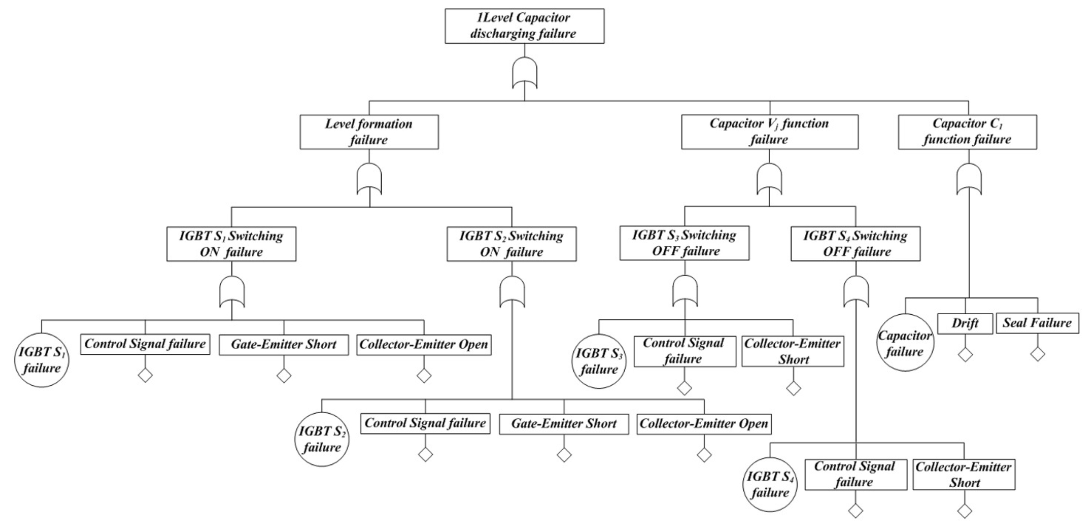
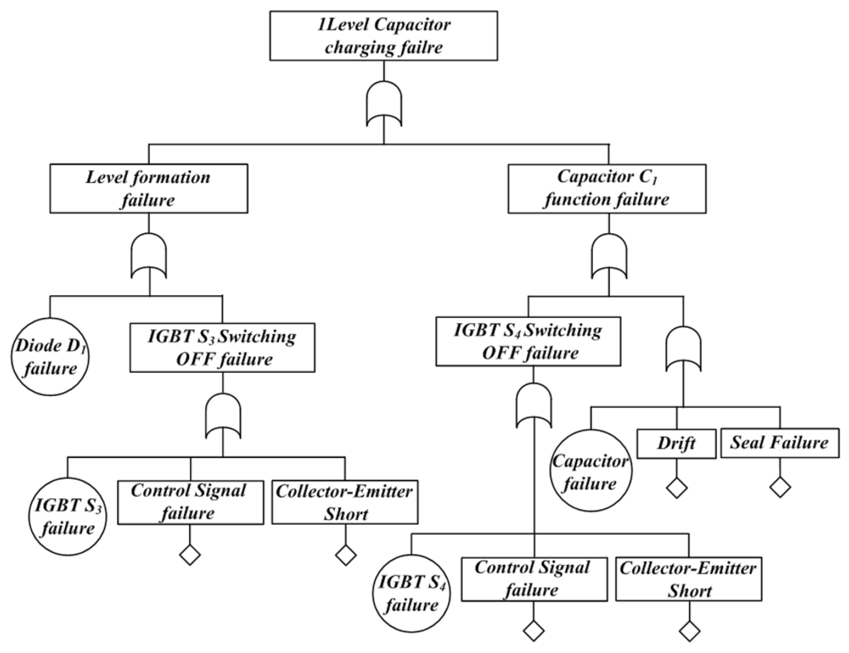
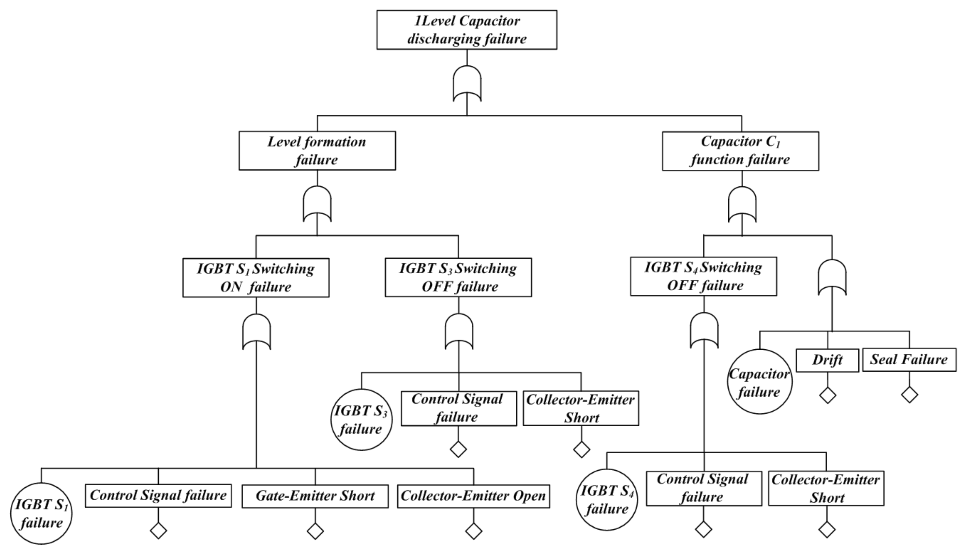
2.2.1. DCC Fault Tree Design
2.2.2. FCC Fault Tree Design
2.2.3. TNPC Fault Tree Design
2.3. Part Failure Rate Based on MIL-HDBK-217F
2.3.1. IGBT Failure Rate
2.3.2. Capacitor Failure Rate
2.3.3. Diode Failure Rate
3. Reliability Analysis Based on Operating Characteristics
3.1. Analysis of Failure Rate of Multi-Level Inverter Using Fault-Tree
3.2. Comparison of DCC, FCC, TNPC, and MMC
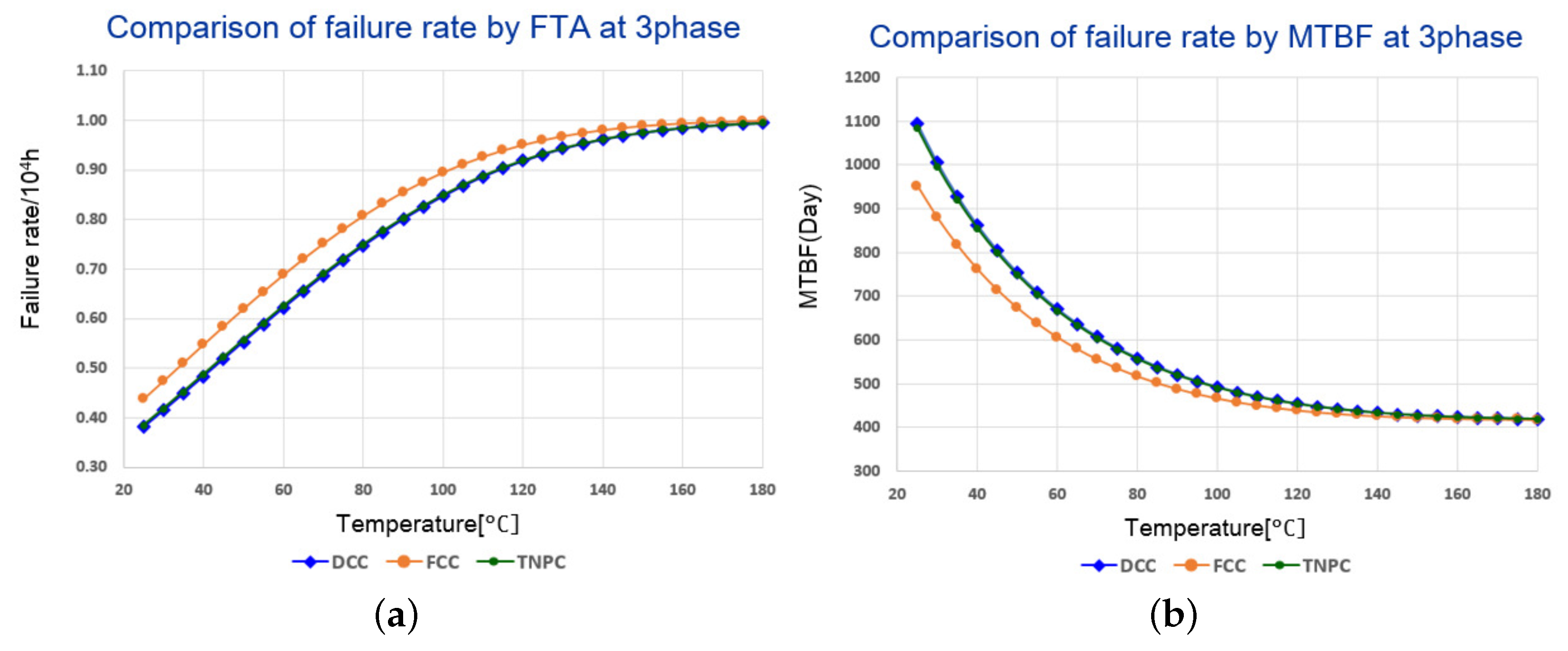
3.2.1. Comparison of Failure Rates based on PCA and FTA
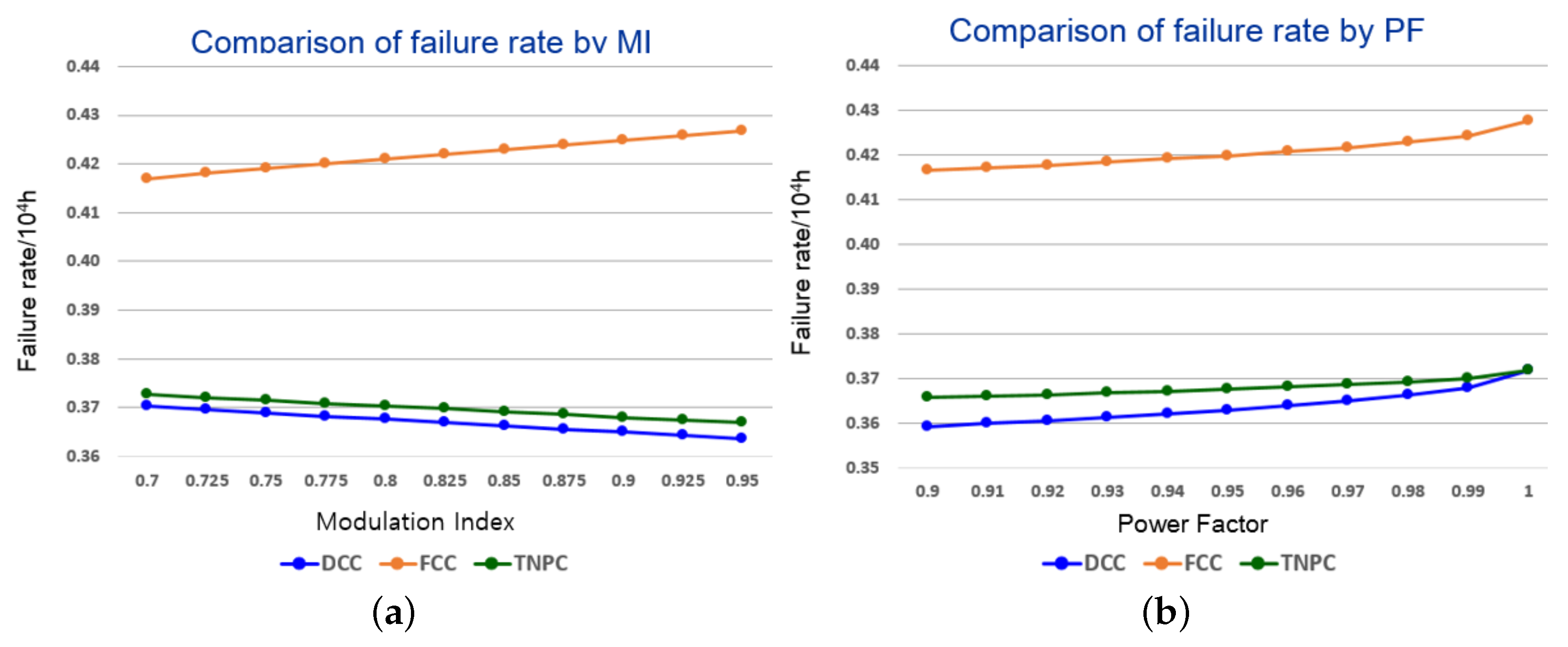
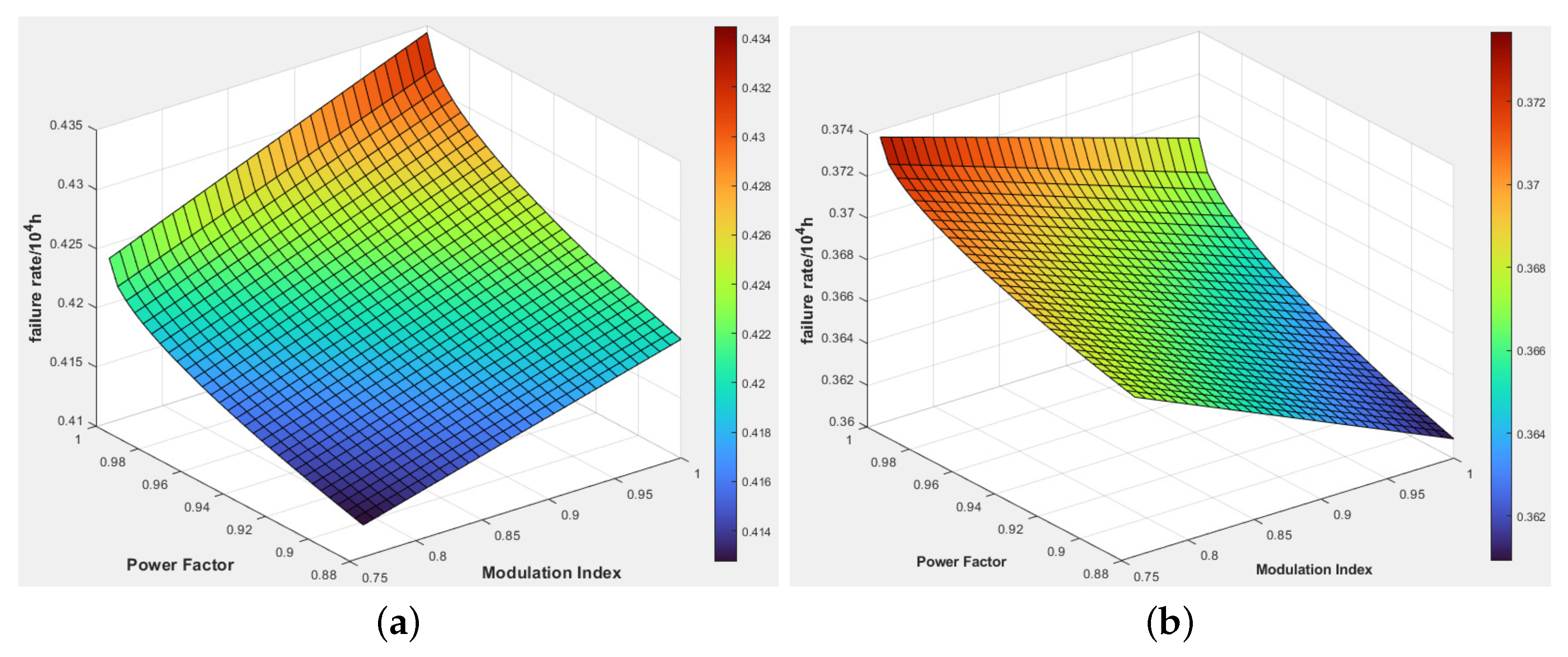
3.2.2. Comparison of Failure Rate Based on Modulation Ratio and Power Factor
4. Conclusions
Author Contributions
Funding
Data Availability Statement
Conflicts of Interest
References
- Mateja, K.; Skarka, W.; Drygała, A. Efficiency Decreases in a Laminated Solar Cell Developed for a UAV. Materials 2022, 15, 8774. [Google Scholar] [CrossRef]
- Arum, S.C.; Grace, D.; Mitchell, P.D.; Zakaria, M.D.; Morozs, N. Energy management of solar-powered aircraft-based high altitude platform for wireless communications. Electronics 2020, 9, 179. [Google Scholar] [CrossRef]
- Pham, K.L.; Leuchter, J.; Bystricky, R.; Andrle, M.; Pham, N.N.; Pham, V.T. The study of electrical energy power supply system for UAVs based on the energy storage technology. Aerospace 2022, 9, 500. [Google Scholar] [CrossRef]
- Pupadubsin, R.; Mecrow, B.C.; Widmer, J.D.; Steven, A. Smooth voltage pwm for vibration and acoustic noise reduction in switched reluctance machines. IEEE Trans. Energy Convers. 2020, 36, 1578–1588. [Google Scholar] [CrossRef]
- Huang, Y.; Xu, Y.; Zhang, W.; Zou, J. Hybrid RPWM technique based on modified SVPWM to reduce the PWM acoustic noise. IEEE Trans. Power Electron. 2018, 34, 5667–5674. [Google Scholar] [CrossRef]
- Villa, T.F.; Gonzalez, F.; Miljievic, B.; Ristovski, Z.D.; Morawska, L. An overview of small unmanned aerial vehicles for air quality measurements: Present applications and future prospectives. Sensors 2016, 16, 1072. [Google Scholar] [CrossRef]
- Li, Y.; Ding, Q.; Li, K.; Valtchev, S.; Li, S.; Yin, L. A survey of electromagnetic influence on UAVs from an EHV power converter stations and possible countermeasures. Electronics 2021, 10, 701. [Google Scholar] [CrossRef]
- Afsharnia, F. Failure rate analysis. In Failure Analysis and Prevention; IntechOpen: London, UK, 2017. [Google Scholar]
- Krasich, M. How to estimate and use MTTF/MTBF would the real MTBF please stand up? In Proceedings of the 2009 Annual Reliability and Maintainability Symposium, Fort Worth, TX, USA, 26–29 January 2009; IEEE: New York, NY, USA, 2009; pp. 353–359. [Google Scholar]
- Zhou, W.; Wang, M.; Wu, Q.; Xi, L.; Xiao, K.; Bhat, K.P.; Chen, C. Accelerated life testing method of metallized film capacitors for inverter applications. IEEE Trans. Transp. Electrif. 2020, 7, 37–49. [Google Scholar] [CrossRef]
- Wu, Q.; Wang, M.; Zhou, W.; Lu, X.; Xiao, K.; Bhat, K.P.; Chen, C. Traction inverter highly accelerated life testing with high-temperature stress. IEEE Trans. Transp. Electrif. 2020, 7, 304–316. [Google Scholar] [CrossRef]
- Sangwongwanich, A.; Shen, Y.; Chub, A.; Liivik, E.; Vinnikov, D.; Wang, H.; Blaabjerg, F. Design for accelerated testing of DC-link capacitors in photovoltaic inverters based on mission profiles. IEEE Trans. Ind. Appl. 2020, 57, 741–753. [Google Scholar] [CrossRef]
- Dhople, S.V.; Davoudi, A.; Chapman, P.L.; Domínguez-García, A.D. Integrating photovoltaic inverter reliability into energy yield estimation with Markov models. In Proceedings of the 2010 IEEE 12th Workshop on Control and Modeling for Power Electronics (COMPEL), Boulder, CO, USA, 28–30 June 2010; IEEE: New York, NY, USA, 2010; pp. 1–5. [Google Scholar]
- Cristaldi, L.; Khalil, M.; Soulatintork, P. A root cause analysis and a risk evaluation of PV balance of system failures. Acta Imeko 2017, 6, 113–120. [Google Scholar] [CrossRef]
- Theristis, M.; Papazoglou, I.A. Markovian reliability analysis of standalone photovoltaic systems incorporating repairs. IEEE J. Photovolt. 2013, 4, 414–422. [Google Scholar] [CrossRef]
- Song, Y.; Wang, B. Survey on reliability of power electronic systems. IEEE Trans. Power Electron. 2012, 28, 591–604. [Google Scholar] [CrossRef]
- Wylie, J.; Merlin, M.C.; Green, T.C. Analysis of the effects from constant random and wear-out failures of sub-modules within a modular multi-level converter with varying maintenance periods. In Proceedings of the 2017 19th European Conference on Power Electronics and Applications (EPE’17 ECCE Europe), Warsaw, Poland, 11–14 September 2017; IEEE: New York, NY, USA, 2017; p. P1. [Google Scholar]
- Bakouch, H.S.; Ristić, M.M.; Asgharzadeh, A.; Esmaily, L.; Al-Zahrani, B.M. An exponentiated exponential binomial distribution with application. Stat. Probab. Lett. 2012, 82, 1067–1081. [Google Scholar] [CrossRef]
- Choudhary, K.; Sidharthan, P. Reliability prediction of Electronic Power Conditioner (EPC) using MIL-HDBK-217 based parts count method. In Proceedings of the 2015 International Conference on Computer, Communication and Control (IC4), Indore, India, 10–12 September 2015; IEEE: New York, NY, USA, 2015; pp. 1–4. [Google Scholar]
- Krishnachaitanya, D.; Chitra, A. Quantitative analysis of asymmetric multilevel inverters with reduced device count from reliability and cost function perspective—A review. IEEE Trans. Power Electron. 2021, 36, 11068–11086. [Google Scholar] [CrossRef]
- Frey, D.; Palladino, J.; Sullivan, J.; Atherton, M. Part count and design of robust systems. Syst. Eng. 2007, 10, 203–221. [Google Scholar] [CrossRef]
- Ruijters, E.; Stoelinga, M. Fault tree analysis: A survey of the state-of-the-art in modeling, analysis and tools. Comput. Sci. Rev. 2015, 15, 29–62. [Google Scholar] [CrossRef]
- Shalev, D.M.; Tiran, J. Condition-based fault tree analysis (CBFTA): A new method for improved fault tree analysis (FTA), reliability and safety calculations. Reliab. Eng. Syst. Saf. 2007, 92, 1231–1241. [Google Scholar] [CrossRef]
- Kang, F.S.; Song, S.G. Life-cycle expectation using fault-tree analysis for improved hybrid submodule in HVDC system. Electronics 2021, 10, 133. [Google Scholar] [CrossRef]
- Kabir, S. An overview of fault tree analysis and its application in model based dependability analysis. Expert Syst. Appl. 2017, 77, 114–135. [Google Scholar] [CrossRef]
- Spertino, F.; Amato, A.; Casali, G.; Ciocia, A.; Malgaroli, G. Reliability analysis and repair activity for the components of 350 kW inverters in a large scale grid-connected photovoltaic system. Electronics 2021, 10, 564. [Google Scholar] [CrossRef]
- Catelani, M.; Ciani, L.; Bartolini, A.; Del Rio, C.; Guidi, G.; Patrizi, G. Reliability analysis of wireless sensor network for smart farming applications. Sensors 2021, 21, 7683. [Google Scholar] [CrossRef] [PubMed]
- Yeo, S.C.; Kang, F.S. Fault-tree based failure-rate analysis for boost converter and interleaved boost converter. J. Electr. Eng. Technol. 2019, 14, 2375–2387. [Google Scholar] [CrossRef]
- Khairnar, D.D.; Deshmukh, V. Performance Analysis of Diode Clamped 3 Level MOSFET Based Inverter. Int. Electr. Eng. J. (IEEJ) 2014, 5, 1484–1489. [Google Scholar]
- Ahmadi, S.; Poure, P.; Saadate, S.; Khaburi, D.A. Fault tolerance analysis of five-level neutral-point-clamped inverters under clamping diode open-circuit failure. Electronics 2022, 11, 1461. [Google Scholar] [CrossRef]
- Barros, L.A.; Martins, A.P.; Pinto, J.G. A comprehensive review on modular multilevel converters, submodule topologies, and modulation techniques. Energies 2022, 15, 1078. [Google Scholar] [CrossRef]
- Alepuz, S.; Busquets-Monge, S.; Nicolás-Apruzzese, J.; Filbà-Martínez, À.; Bordonau, J.; Yuan, X.; Kouro, S. A survey on capacitor voltage control in neutral-point-clamped multilevel converters. Electronics 2022, 11, 527. [Google Scholar] [CrossRef]
- Taul, M.G.; Pallo, N.; Stillwell, A.; Pilawa-Podgurski, R.C. Theoretical analysis and experimental validation of flying-capacitor multilevel converters under short-circuit fault conditions. IEEE Trans. Power Electron. 2021, 36, 12292–12308. [Google Scholar] [CrossRef]
- Shukla, A.; Ghosh, A.; Joshi, A. Flying-capacitor-based chopper circuit for dc capacitor voltage balancing in diode-clamped multilevel inverter. IEEE Trans. Ind. Electron. 2009, 57, 2249–2261. [Google Scholar] [CrossRef]
- Salem, M.; Richelli, A.; Yahya, K.; Hamidi, M.N.; Ang, T.Z.; Alhamrouni, I. A comprehensive review on multilevel inverters for grid-tied system applications. Energies 2022, 15, 6315. [Google Scholar] [CrossRef]
- Zygmanowski, M. Detailed Power Loss Analysis of T-Type Neutral Point Clamped Converter for Reactive Power Compensation. Electronics 2022, 11, 2129. [Google Scholar] [CrossRef]
- Zhang, Z.; Anthon, A.; Andersen, M.A. Comprehensive loss evaluation of neutral-point-clamped (NPC) and T-Type three-level inverters based on a circuit level decoupling modulation. In Proceedings of the 2014 International Power Electronics and Application Conference and Exposition, Shanghai, China, 5–8 November 2014; IEEE: New York, NY, USA, 2014; pp. 82–87. [Google Scholar]
- Bahrami, A.; Narimani, M. A new five-level T-type nested neutral point clamped (T-NNPC) converter. IEEE Trans. Power Electron. 2019, 34, 10534–10545. [Google Scholar] [CrossRef]
- Zhang, J.; Xu, S.; Din, Z.; Hu, X. Hybrid multilevel converters: Topologies, evolutions and verifications. Energies 2019, 12, 615. [Google Scholar] [CrossRef]
- Rojas, C.A.; Kouro, S.; Inzunza, R.; Mitsugi, Y.; Alcaide, A.M. Harmonic Impedance Model of Multiple Utility-Interactive Multilevel Photovoltaic Inverters. Energies 2022, 15, 9462. [Google Scholar] [CrossRef]
- Mou, H.; Hu, W.; Sun, Y.; Zhao, G. A comparison and case studies of electronic product reliability prediction methods based on handbooks. In Proceedings of the 2013 International Conference on Quality, Reliability, Risk, Maintenance, and Safety Engineering (QR2MSE), Emeishan, China, 15–18 July 2013; IEEE: Piscataway, NJ, USA, 2013; pp. 112–115. [Google Scholar]
- Jones, J.; Hayes, J. A comparison of electronic-reliability prediction models. IEEE Trans. Reliab. 1999, 48, 127–134. [Google Scholar] [CrossRef]
- Valentine, N.; Das, D.; Pecht, M.; Pecht, M. Failure mechanisms of insulated gate bipolar transistors (IGBTs). In Proceedings of the NREL Photovoltaic Reliability Workshop, Center for Advanced Life Cycle Engineering (CALCE), Golden, CO, USA, 24–27 February 2015; University of Maryland: College Park, MD, USA, 2015. [Google Scholar]
- Pokorni, S. Reliability prediction of electronic equipment: Problems and experience. In Proceedings of the 7th International Scientific Conference on Defensive Technologies OTEH, Belgrade, Serbia, 6–7 October 2016; pp. 6–7. [Google Scholar]
- Lee, K.; Shin, H.; Choi, J. Comparative analysis of power losses for 3-Level NPC and T-type inverter modules. In Proceedings of the 2015 IEEE International Telecommunications Energy Conference (INTELEC), Osaka, Japan, 18–22 October 2015; IEEE: New York, NY, USA, 2015; pp. 1–6. [Google Scholar]
- Tehrani, K.A.; Rasoanarivo, I.; Sargos, F.M. Power loss calculation in two different multilevel inverter models (2DM2). Electr. Power Syst. Res. 2011, 81, 297–307. [Google Scholar] [CrossRef]


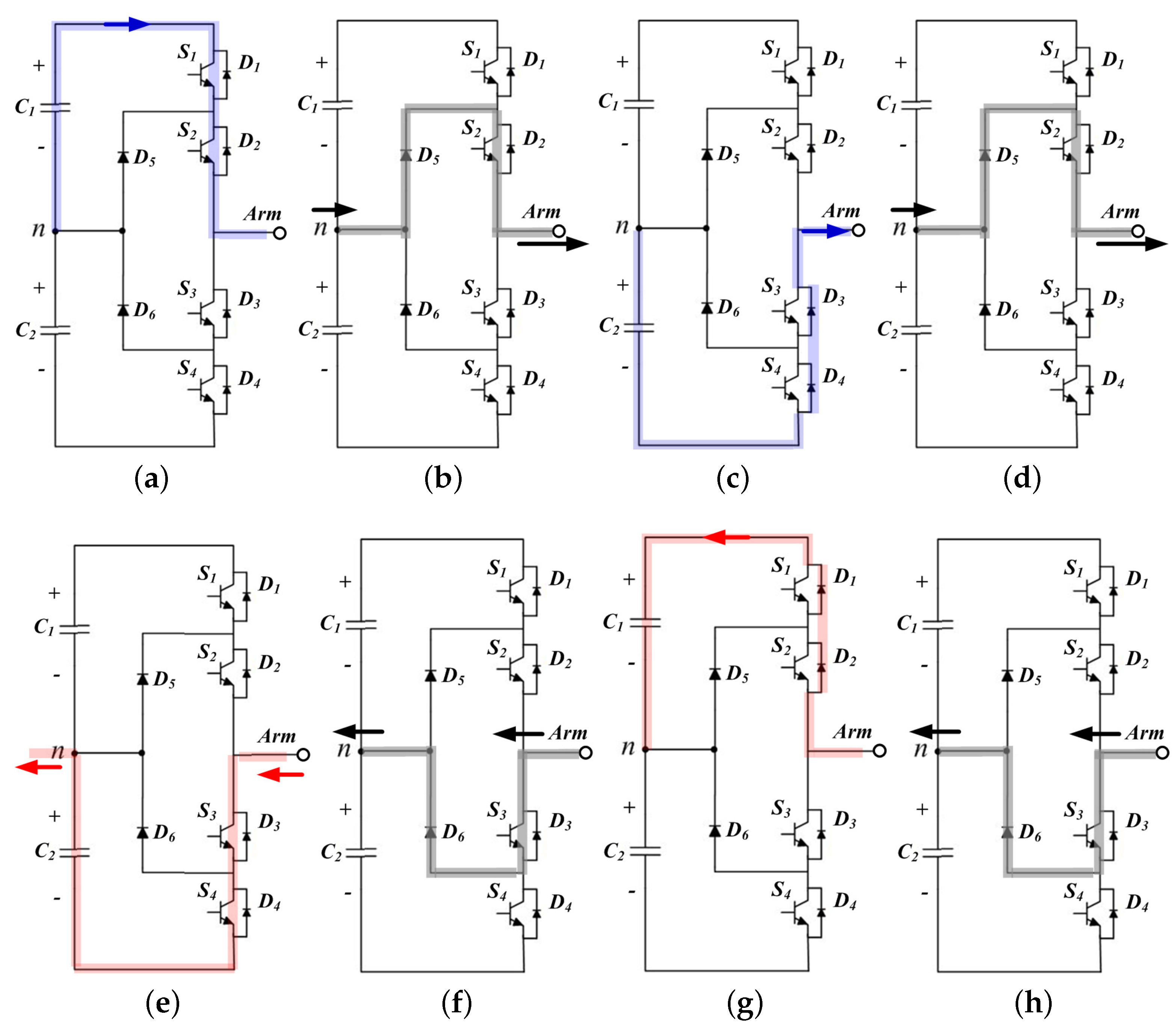
| Current | Voltage | Level | On Switch | Power Flow | Note |
|---|---|---|---|---|---|
| Polarity | Polarity | Formation | Operation | ||
| Positive | Positive | 1 level | S1, S2 | C1 discharge | Figure 1a |
| Zero level | S2, D5 | Freewheeling | Figure 1b | ||
| Negative | −1 level | D3, D4 | C2 charge | Figure 1c | |
| Zero level | D5, S2 | Freewheeling | Figure 1d | ||
| Negative | Positive | −1 level | S3, S4 | C2 discharge | Figure 1e |
| Zero level | S3, D6 | Freewheeling | Figure 1f | ||
| Negative | 1 level | D1, D2 | C1 charge | Figure 1g | |
| Zero level | S3, D6 | Freewheeling | Figure 1h |
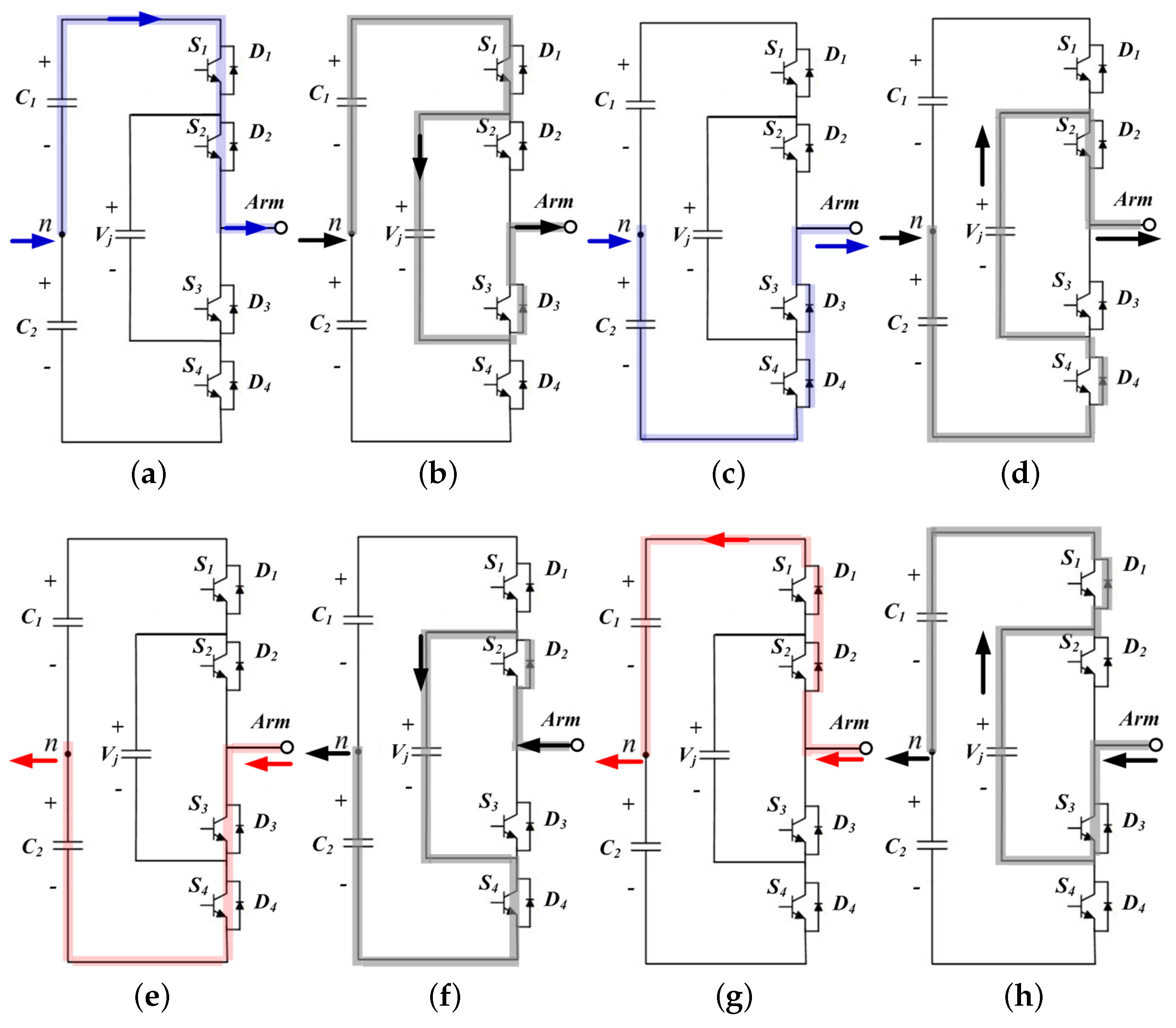
| Current | Voltage | Level | On Switch | Power Flow | Note |
|---|---|---|---|---|---|
| Polarity | Polarity | Formation | Operation | ||
| Positive | Positive | 1 level | S1, S2 | C1 discharge | Figure 2a |
| Zero level | S1, D3 | charge | Figure 2b | ||
| Negative | −1 level | D3, D4 | C2 charge | Figure 2c | |
| Zero level | D4, S2 | discharge | Figure 2d | ||
| Negative | Positive | −1 level | S3, S4 | C2 discharge | Figure 2e |
| Zero level | D2, S4 | charge | Figure 2f | ||
| Negative | 1 level | D1, D2 | C1 charge | Figure 2g | |
| Zero level | D1, S3 | discharge | Figure 2h |
| Current | Voltage | Level | On Switch | Power Flow | Note |
|---|---|---|---|---|---|
| Polarity | Polarity | Formation | Operation | ||
| Positive | Positive | 1 level | S1 | C1 discharge | Figure 3a |
| Zero level | S1, D3 | freewheeling | Figure 3b | ||
| Negative | −1 level | D4 | C2 charge | Figure 3c | |
| Zero level | S2, D3 | freewheeling | Figure 3d | ||
| Negative | Positive | −1 level | S4 | C2 discharge | Figure 3e |
| Zero level | D2, S4 | freewheeling | Figure 3f | ||
| Negative | 1 level | D1 | C1 charge | Figure 3g | |
| Zero level | D2, S3 | freewheeling | Figure 3h |
| Temp | Failures/ h | |||
|---|---|---|---|---|
| IGBT | Diode (in IGBT) | Diode (DCC) | Capacitor | |
| 25 (−40) | 0.02629370 | 0.00430735 | 0.00430735 | 0.00013098 |
| 85 (20) | 0.07769091 | 0.02450135 | 0.02450135 | 0.00060481 |
| 125 (60) | 0.13335677 | 0.05835091 | 0.05835091 | 0.00123467 |
| 150 (85) | 0.17742397 | 0.09234005 | 0.09234005 | 0.00177865 |
| 180 (115) | 0.23966516 | 0.14981587 | 0.14981587 | 0.00259040 |
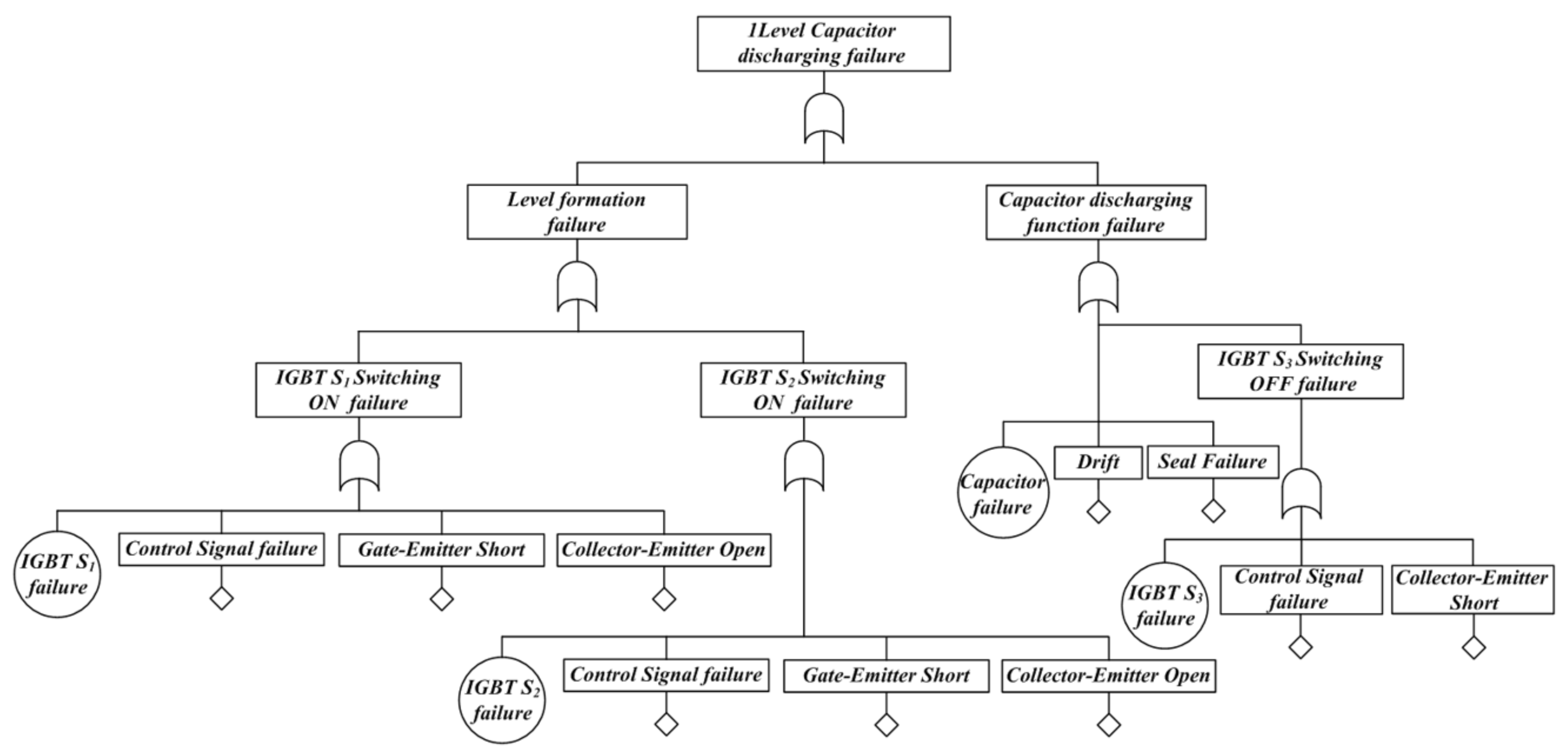
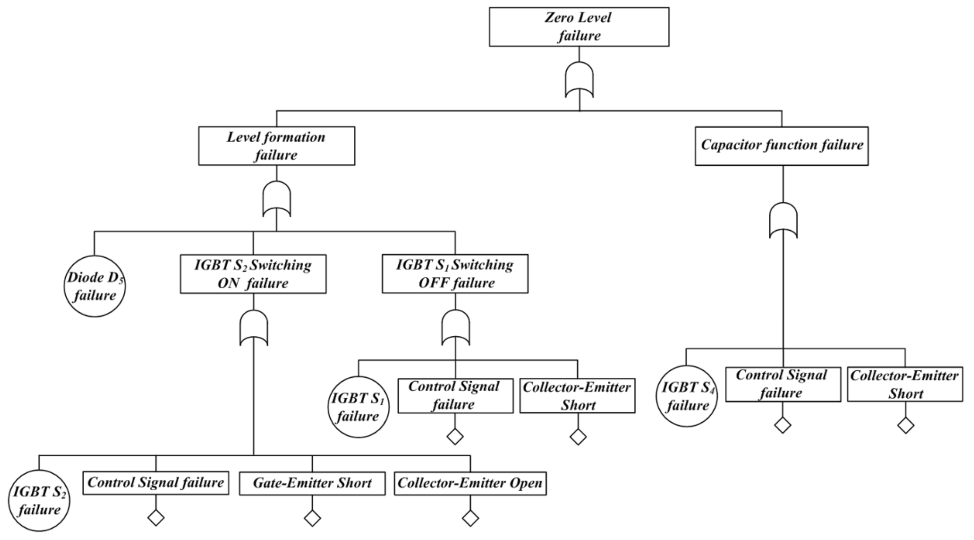
| Topology | Parts Type | 1-Level Discharging | 1-Level Charging | Zero-Level |
|---|---|---|---|---|
| Failure (M1) | Failure (M2) | Failure (M3) | ||
| DCC | IGBT | 3 | 1 | 3 |
| Diode(in IGBT) | 0 | 2 | 0 | |
| Diode | 0 | 0 | 1 | |
| Capacitor | 1 | 1 | 0 | |
| FCC | IGBT | 4 | 2 | 3 |
| Diode(in IGBT) | 0 | 2 | 1 | |
| Capacitor | 1 | 1 | 2 | |
| TNPC | IGBT | 3 | 2 | 3 |
| Diode(in IGBT) | 0 | 1 | 1 | |
| Capacitor | 1 | 1 | 0 |
| Topology | Parts Type and Number | |||
|---|---|---|---|---|
| IGBT | Diode(in IGBT) | Diode(DCC) | Capacitor | |
| DCC | 4 | 4 | 2 | 2 |
| FCC | 4 | 4 | 0 | 3 |
| TNPC | 4 | 4 | 0 | 2 |
Disclaimer/Publisher’s Note: The statements, opinions and data contained in all publications are solely those of the individual author(s) and contributor(s) and not of MDPI and/or the editor(s). MDPI and/or the editor(s) disclaim responsibility for any injury to people or property resulting from any ideas, methods, instructions or products referred to in the content. |
© 2023 by the authors. Licensee MDPI, Basel, Switzerland. This article is an open access article distributed under the terms and conditions of the Creative Commons Attribution (CC BY) license (https://creativecommons.org/licenses/by/4.0/).
Share and Cite
Lee, J.-H.; Jun, H.-S.; Park, H.-M.; Park, J.-H.; Lim, S.-K. Reliability Analysis of a Multilevel Inverter Applied to Stratospheric Drones Using Fault Tree Analysis. Electronics 2023, 12, 4952. https://doi.org/10.3390/electronics12244952
Lee J-H, Jun H-S, Park H-M, Park J-H, Lim S-K. Reliability Analysis of a Multilevel Inverter Applied to Stratospheric Drones Using Fault Tree Analysis. Electronics. 2023; 12(24):4952. https://doi.org/10.3390/electronics12244952
Chicago/Turabian StyleLee, Jung-Hwan, Hyang-Sig Jun, Hee-Mun Park, Jin-Hyun Park, and Sang-Kil Lim. 2023. "Reliability Analysis of a Multilevel Inverter Applied to Stratospheric Drones Using Fault Tree Analysis" Electronics 12, no. 24: 4952. https://doi.org/10.3390/electronics12244952
APA StyleLee, J.-H., Jun, H.-S., Park, H.-M., Park, J.-H., & Lim, S.-K. (2023). Reliability Analysis of a Multilevel Inverter Applied to Stratospheric Drones Using Fault Tree Analysis. Electronics, 12(24), 4952. https://doi.org/10.3390/electronics12244952