Abstract
This contribution presents the AM/AM and AM/PM characteristics of a 6-bit Phase and Amplitude Setting Circuit realized in Gallium Nitride technology and operating at the Ku band. A test bench, based on three vector receivers and an absolute power reference, has been purposely devised to capture the deviation with respect to the linear behavior (known by the S-parameters) for both the magnitude and the phase of the vector response. The complete 64-state constellation is reported up to a 37 dBm of input power level, at which the effects of the static AM/AM and AM/PM distortion become evident, with about 3 dB of gain compression and 2.7 deg of phase conversion. The key figure of merit of the proposed test bench is the capability of operating with very high driving power levels (potentially up to 41 dBm), with possible applications in phased arrays, AESAs, and other signal conditioning systems.
1. Introduction
Gallium Nitride (GaN) has become the industry standard semiconductor for microwave and millimeter-wave circuits in high-end electronic systems utilized in space communications. More specifically, GaN technology is currently utilized for signal conditioning, shaping, and generation circuits, including mixers [1,2], voltage-controlled oscillators (VCO) [3,4], phase shifters (PS) [5,6,7,8,9], and attenuators (ATT) [10] at microwave and millimeter-wave frequencies. In particular, when combined, the latter two listed functionalities realize the Phase and Amplitude Setting circuits (PASs), key components in Radio Frequency (RF) front ends, and more specifically, for phased array systems. In addition to millimeter-wave and microwave circuits in high-end electronic systems, GaN has been extensively utilized in the fabrication of optoelectronic devices, such as lasers [11,12,13,14,15], light emitting diodes (LEDs) [16,17,18,19,20,21], and solar cells [22,23,24].
Phased arrays can be categorized into three architectures: passive, active, and digital [25]. Each has its proper field of application in which it is featured by better figures of merit compared to the others. In particular, the passive architecture uses a centralized high-power transmit amplifier capable of kW peak power levels (typically realized by a klystron vacuum tube or a traveling wave tube amplifier) and requires the use of low-loss beamformers and phase shifters because RF losses on the output path from the transmit amplifier to free space translate directly into signal loss and, thus, reduced radar sensitivity. Ferrite phase shifters are commonly used in passive arrays since they can handle very high levels of microwave power with very low insertion loss; however, they are bulky, and the overall system would benefit by replacing them with monolithic ones. This is why there is an increasing interest in the realization of GaN phase shifters, and this is one of the reasons why the non-linear characterization of the GaN PAS control circuits is of interest. Furthermore, the availability of multifunctional monolithic microwave integrated circuits (MMICs) allowed the Active Electronically Scanned Array (AESA) System to present a technological breakthrough in improved reliability, reconfigurability, performance, wideband capabilities, and ease of installation in space communication systems [26]. To follow technological advancements, thorough characterization of RF front ends is required, as the front end always operates at higher frequencies, owing to the ever-growing demand for spectrally efficient wireless communication chips [27,28,29,30]. In addition to measuring the linear response, achieved through scattering parameters (S-parameters), it is also important to characterize the performance of the signal conditioning circuits in terms of non-linear figures of merit, such as the amplitude-to-amplitude (AM/AM) conversion and the amplitude-to-phase (AM/PM) conversion characteristics. While the AM/AM characterization can be easily obtained via scalar power measurements, the AM/PM characterization presents a challenge that requires phase-detecting approaches and is usually performed by a Vector Network Analyzer (VNA), even if some alternative approaches have been proposed using a spectrum analyzer or oscilloscopes.
Additionally, in the case of passive Device Under Test (DUT) on GaN, capable of high-power handling, very high input power levels are required to drive the device into its non-linear region. Most literature has focused on AM/AM and AM/PM characterization of power amplifiers (PAs), as discussed in [28,29,31,32,33,34,35,36,37,38]. However, only a few articles deal with AM/AM characterization, and even fewer deal with AM/PM characterization of passive circuits. Some examples are presented in [39,40,41,42,43,44,45] and [39,46,47], respectively. Specialized test benches have been developed and somehow exploited for amplifiers [28,31,32,33,34,35,36,37,48,49], but not for passive circuits. No reported works explicitly focus on AM/PM characterization of PAS GaN HEMT circuits at such high input power (37 dBm) and frequency ranges (Ku Band, 12 GHz to 18 GHz).
Table 1 reports some significant references dealing with the measurements of the AM/PM for different kinds of MMICs.

Table 1.
Comparison table of the different references dealing with AM/AM and AM/PM characteristics for different devices.
In this contribution, we propose a rather standard test bench based on a VNA and aimed at characterizing the static AM/AM and AM/PM conversions of a 6-bit PAS MMIC.
AM/AM and AM/PM are standard figures of merit typically used to describe the non-linear behavior of a device. In particular, AM/AM represents the deviation of the amplitude response of the device from linear behavior. Typically, by increasing the input power level of 1 dB at a certain frequency, we expect the output power level to increase by 1 dB; if this is not the case, non-linearities contribute to the amplitude response. Conversely, AM/PM represents the deviation of the phase response from linear behavior. At a certain frequency, we expect a constant phase response with respect to the input power level; if this does not occur, the phase response is affected by non-linearities.
The architecture of the considered PAS circuit is reported in Figure 1, showing the actual position of the phase-shifting and amplitude-setting cells within the same MMIC. Details on this kind of circuit are provided, for instance, in [10]. The peculiarity of the measurement setup is its capability of capturing the static conversion curves of GaN passive circuits, thus requiring a very high level of linearity of the test bench building blocks. The manuscript is organized as follows: Section 2 is devoted to the measurement setup, Section 3 addresses the calibration/de-embedding technique, and Section 4 presents the measured results. Finally, some concluding remarks are given in Section 5.
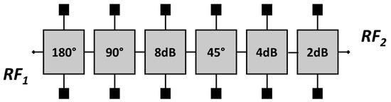
Figure 1.
Block diagram of the Device Under Test (DUT).
2. Measurement Setup
The measurement test bench is based on an Anritsu 37397D VNA, together with a power amplifier (Erzia HPA-0600-1800-40-E, capable of 41 dBm [50] of output power), two external couplers (HP87301D), three fixed attenuators (HP8490D), and a 50 Ohm power termination. Figure 2 depicts the photograph of the measurement setup.
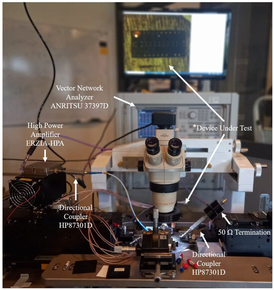
Figure 2.
Photo of the measurement setup for AM/AM and AM/PM characterization.
In a more detailed perspective, Figure 3 illustrates the external connections through jumpers on the front panel of the VNA, enabling access to the internal receivers and source. As depicted in the figure, the excitation signal was derived from port-1 of the VNA (rather than directly from the jumpers) to take advantage of the internal attenuators [51]. Regarding the receiver, in addition to the b1 and b2 detectors needed to sample the input and output waves, respectively, a third receiver, a1, was also used to ease the phase lock condition, as illustrated in Figure 4. The latter figure reports the architecture of the test bench, also showing the power splitter internal to the VNA, whose purpose is to ease the phase lock of the receiver (to the internal source) and to level the source. In the same figure, the power level at the relevant sections is also reported, assuming 35 dBm at the input of the DUT. This simple power budget analysis was required to avoid failures at the VNA internal receivers and guarantee the required power level at the input of the DUT. Additionally, it was ensured that the power levels do not exceed 20 dBm at peak value for the ‘a’ receiver and 27 dBm at peak value for the ‘b’ receivers.
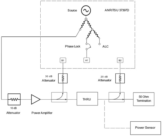
Figure 3.
The architecture of the test bench represented during the calibration phase (with a ‘thru’ connection in place of the DUT). The dotted line represents the alternative path required during one of the two calibration steps.
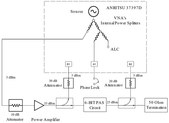
Figure 4.
Test bench architecture also shows the power splitter internal to the VNA. The power level at the relevant sections is reported, assuming 35 dBm at the input of the DUT.
Taking into account the coupling factors of the available directional couplers, the attenuators required to satisfy the above-mentioned conditions were properly dimensioned and explicitly reported in the figure.
Given the comparatively large number of states to measure, a mixed analogue/digital Input (IO) board equipped with an ethernet interface was purposely procured and adapted to the task, as shown in Figure 5.
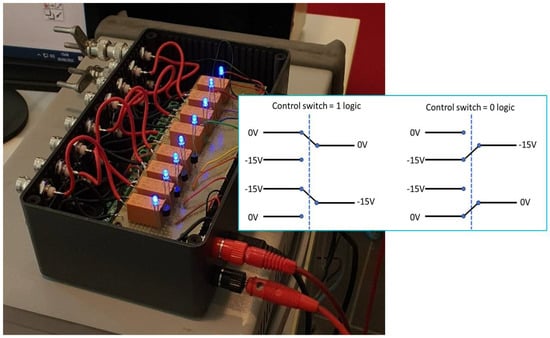
Figure 5.
Relay board interface. The inset reports the circuit topology implementing the control voltages required by the attenuation and phase-shifting cells. The relays are activated by LabView through TTL signals provided by the digital IO board.
A LabVIEW(R) program controlled all the hardware in this measurement setup through the General-Purpose Interface Bus (GPIB) cables and Local Area Network (LAN) cables, whereas the post-processing was implemented in MATLAB.
In addition to the non-linear measurements needed to characterize the AM/AM and AM/PM conversion, the PAS was preliminarily measured in terms of scattering parameters using the Anritsu 37397D in its standard configuration and calibrated with a standard Short-Open-Load-Through (SOLT) calibration on a Calibration Substrate (CS)-5 from the GGB Picoprobe. As detailed in the subsequent sections, the S-parameters allow us to accurately determine the attenuation and phase shift values synthesized by the PAS in linear operation.
3. Calibration of the Test Bench
The VNA detectors’ readings represent the DUT behavior only once the calibration is performed [52]. This section describes the determination of the required correction factors and debates the limitations of the proposed approach. The calibration process consists of two distinct phases, as also reported in Figure 3, in which a thru connection substitutes the DUT:
- In the first step, acquisitions were made from 12 GHz to 16 GHz with a 1 GHz step at a fixed −20 dBm source power level and stored in a file (labeled CALA file) collecting the readings made by the detector-b1 and the USB power sensor U2022XA (the dotted path in Figure 2).
- In the second step, acquisitions were made from 12 GHz to 16 GHz with a 1 GHz step and from −20 dBm up to 10 dBm (to verify the linearity of the driver amplifier) while setting an exit condition at 1 dB of gain compression of the driver amplifier. This second set of data is stored in a file (labeled CALB file), collecting the readings made using the detectors a1, b1, and b2 (refer to Figure 3).
The first step allows for setting an absolute power reference against which the correction factors for the VNA’s readings (b1 and b2) can be computed. The additional readings made by the a1 detector are needed only to provide a stable phase reference, as discussed later in the text. The power sweep in the second step, even if not strictly required for calibration purposes, allowed for ascertaining the linearity of the driver amplifier.
Off-line, during the post-processing, the raw measurements performed on the thru and on the DUT are imported from the three files (CALA, CALB, and DUT), and then the correction factors are computed and applied to the raw readings.
In greater detail, in the first post-processing step, the readings made by the VNA and the power sensor are considered (with a thru in place of the DUT). Comparing these two readings allows for obtaining a correction factor for the b1-detector, setting the reference plane at the coaxial connection of the output probe. Then, the reference plane is shifted to the center of the thru; in formulae, the additive correction factor for the detector b1 is:
in which are the readings (in dBm) made by the sensor and are the readings (in dBm) made by the VNA, both stored in the CALA file, whereas is the probe loss (in dB) determined through an unterminating procedure and nearly equal to 0.6 dB all over the measurement band. In a second post-processing step, the readings made by the VNA through the detectors a1, b1, and b2 are considered (with a thru in place of the DUT). Specifically, the CALB file includes the following data: , and . The readings are normalized to overcoming, in this way, the errors associated with the arbitrary phase of the internal source and simultaneously allowing for locking the receiver. The additive correction factor, , for the b2 detector is:
in which , and are the magnitude readings in dBm taken by the VNA and stored in the CALB file. The previous equation is computed at a fixed source power level, operating under the assumption of receivers’ linearity and encompassing a frequency sweep from 12 GHz to 16 GHz with increments of a 1 GHz step. Similarly, for phase:
in which is unknown since the power sensor does not provide a phase reference. However, what is needed is not the absolute phase, but the phase shift introduced by the DUT:
in which both and cancel out and must not be known. In the previous relation, the superscript ‘D’ stands for data stored in the DUT file, whereas the terms and denote a given arbitrary state and the reference state of the 6 bits of the PAS, respectively. In contrast, the rationale described above for the phase correction cannot be applied to the magnitude correction, given that, in this instance, our interest is directed towards ascertaining the output power level at which a specific degree of deviation (either in phase or amplitude) is measured.
Recalling that the linearity of the receivers is assumed, (4) is valid independently of the input power level. However, in the context of linear operation, higher accuracy can be achieved in terms of scattering parameters:
in which the forward scattering parameter also considers the mismatch at the ports and compensates for it. The comparison of (4) and (5), at a low power level, makes possible the computation of a correction factor to be applied to (4), effectively compensating for the mismatch; more simply, the deviation from the linearity measured by the proposed test bench can be used to correct the S-parameters at high power levels. In the case of the phase, for instance, this implies evaluating (4) at a low and given power level; the difference is the deviation to be added to the phase of the S-parameter measurements. Similar considerations apply to correct the magnitude of the S-parameters. The AM/AM and AM/PM distortion characteristics can indeed be measured up to about 40 dBm.
It is worth stressing that the measured AM/AM and AM/PM only relate to the PAS circuit. In fact, there are two directional couplers in the test bench, one allowing sampling of the incident wave to the input of the PAS and the other allowing sampling of the emerging wave from the output of the PAS. As a consequence, even if the driver amplifier distorts the input wave, the PAS figures of merit are derived taking into account and compensating for the effective distorted input wave (as straightforwardly derived from the relations above; (4) in particular).
4. Test Vehicle Measurement Campaign
Measurements were acquired from 12 GHz to 16 GHz with a 1 GHz step, while the internal source’s power was varied from −20 dBm to 10 dBm, with an exit condition on the DUT’s gain compression set to about 3 dB. Even if additional frequency points are available, in this section, graphical data are reported only at 15 GHz. Also, only a subset of the graphs reports the performance of the PAS vs. the input power level (Figure 6 and Figure 7), i.e., the ones in which only the attenuation or phase-shifting cells are switched and not both. Specifically, as a function of the input power level, Figure 6a,b pertain to AM/AM distortion curves, whereas Figure 7a,b relate to AM/PM distortion trends. In contrast to these plots, the remaining graphs, relating to the overall constellation, are shown for a fixed input power level for better readability.
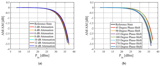
Figure 6.
Measured AM/AM static characteristics were captured under the following conditions: (a) across the spectrum of eight distinct states of the attenuator cells, with the phase shifter configured to its minimum phase shift value; (b) with the attenuator set to its minimum attenuation value, showcasing variations across the eight states of the phase shifter.
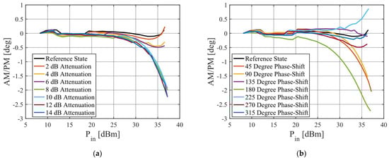
Figure 7.
Characterization of measured AM/PM responses: (a) variation in AM/PM static characteristics across eight distinctive attenuator cell states with the phase shifter configured at minimal phase shift value; (b) AM/PM static characteristics observed across the same eight attenuator cell states, with the attenuator set to its lowest attenuation value and the phase shifter switched over the eight available states.
Figure 6a depicts the measured AM/AM static characteristics for the eight possible states of the attenuator cells with the phase shifter configured to its minimum phase shift value. Under these operating conditions, the maximum measured AM/AM deviation is in the range of 3.2–3.6 dB when the device is driven at 37 dBm of input power. Similarly, Figure 6b reports the measured AM/AM static characteristics for the eight possible states of the phase-shifting cells and the attenuators set to its minimum attenuation value. Under this operating conditions, the maximum measured AM/AM deviation is in the range 3.1–3.7 dB.
Figure 7a,b outline the AM/PM conversion curves for a fixed configuration of the phase-shifting cells and for a fixed configuration of the attenuation cells, respectively. Figure 7 encompasses the response across the 8 + 8 orthogonal states: 8 on the phase axis and 8 on the attenuation axis. Independently of the internal configuration of the MMIC, measurements start deviating from linear behavior at 25 dBm of input power. As can be deducted, the maximum deviation is observed when the 180 deg cell is switched on, with about 2.5 deg at about 3 dB of gain compression.
To provide a clear picture of the non-linear effects on the overall 64 states, for two different power levels (7 dBm and 37 dBm), Figure 8 reports the synthesized attenuation and phase shift values against the nominal (desired) attenuation and nominal phase shift levels. For this purpose, two different kinds of axes were adopted: Figure 8a adopts a Cartesian plot, whereas Figure 8b a polar one, with the latter being more suited to highlight the phase deviation compared to the Cartesian plot. Measurements at 7 dBm of input power level are denoted by asterisks, whereas circles stand for 37 dBm.
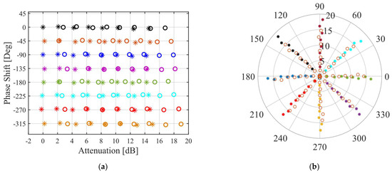
Figure 8.
Measured constellations at 7 dBm (denoted by asterisks) and 37 dBm (represented by circles) input power levels; (a) Cartesian coordinates. (b) Polar coordinates. The radial dimension corresponds to attenuation (dB), while the angular dimension corresponds to phase shift (degrees).
Conversely, Figure 9a,b depict, on a 3D plot, the AM/AM and AM/PM conversion, respectively, with regard to the nominal phase shift and nominal attenuation at 37 dBm. The insights provided by Figure 9a reveal that the AM/AM conversion’s behavior is mainly influenced by the activation status of individual phase cells, demonstrating a relatively subdued response to amplitude cell switching.
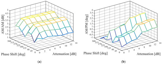
Figure 9.
AM/AM (a) and AM/PM (b) against nominal phase-shift and attenuation levels at approximately 37 dBm.
Different considerations apply to Figure 9b, where it is evident that the AM/PM conversion presents a dependence on both the amplitude- and phase-cell switching. However, in the case of the phase cells, the behavior is monotonic with respect to the increasing attenuation values. In contrast, there is no correlation between the AM/PM deviation (also for the AM/AM deviation) and the absolute phase shifting value, which is mainly dependent on the given cell and not on the value synthesized by the cell.
5. Conclusions
The AM/AM and AM/PM characteristics of a 6-bit PAS circuit realized in GaN technology operating at Ku-band are reported in this contribution. The deviation from the linear behavior of the DUT, known by the measured S-parameters, was calculated through a test bench comprising three vector receivers and an absolute power reference. The linear 64-states constellation at 7 dBm input power level and the distorted one at a 37 dBm input power level are reported: the first, computed by the S-parameters, and the second, derived by the S-parameters, plus the deviation captured by the non-linear test bench. The effectiveness of this contribution relies on further addressing the gap in the research, focusing on the non-linear characterization of passive circuits capable of high-power handling, such as PAS circuits on GaN. Although the proposed implementation presents the advantage of being easily implemented, a more complex calibration algorithm should be considered in possible future implementations for a full vector calibration.
Author Contributions
Conceptualization, W.C. and A.D.; measurement acquisition, F.B. and E.D.A.; software, S.C.; validation, W.C. and P.E.L.; formal analysis, W.C. and A.D.; Device Under Test, P.E.L.; data curation, W.C. and A.D.; writing—original draft preparation, A.D. and W.C.; writing—review and editing, A.D. and W.C.; supervision, E.L.; project administration, E.L. All authors have read and agreed to the published version of the manuscript.
Funding
The contribution described here is performed within the GAMICO project (GAN for Microwave and Millimeter-wave signal Conditioning), funded by Lazio Innova under grant no. A0375-2020-36755, Progetti di Gruppi di Ricerca 2020.
Data Availability Statement
Data is contained within the article.
Conflicts of Interest
The authors declare no conflict of interest. The funders had no role in the design of the study; in the collection, analyses, or interpretation of data; in the writing of the manuscript; or in the decision to publish the results.
References
- De Padova, A.; Longhi, P.E.; Colangeli, S.; Ciccognani, W.; Limiti, E. Design of a GaN-on-Si Single-Balanced Resistive Mixer for Ka-band Satcom. IEEE Microw. Wirel. Compon. Lett. 2019, 29, 56–58. [Google Scholar] [CrossRef]
- Sudow, M.; Andersson, K.; Fagerlind, M.; Thorsell, M.; Nilsson, P.; Rorsman, N. A single-ended resistive X-band AlGaN/GaN HEMT MMIC mixer. IEEE Trans. Microw. Theory Tech. 2008, 56, 2201–2206. [Google Scholar] [CrossRef]
- Cheng, Z.Q.; Cai, Y.; Liu, J.; Zhou, Y.; Lau, K.M.; Chen, K.J. A low phase-noise X-band MMIC VCO using high-linearity and low-noise composite-channel Al0.3Ga0.7N/Al0.05Ga0.95N/GaN HEMTs. IEEE Trans. Microw. Theory Tech. 2007, 55, 23–29. [Google Scholar] [CrossRef]
- Kim, D.; Jeon, S. W- and G-Band GaN Voltage-Controlled Oscillators with High Output Power and High Efficiency. IEEE Trans. Microw. Theory Tech. 2021, 69, 3908–3916. [Google Scholar] [CrossRef]
- Chiu, H.-C.; Chen, C.-M.; Chang, L.-C.; Kao, H.-L. A 5-bit x-band gan hemt-based phase shifter. Electronics 2021, 10, 658. [Google Scholar] [CrossRef]
- Hettak, K.; Ross, T.N.; Cormier, G.; Wight, J.S. A new type of Robust broadband GaN HEMT-based high power high-pass/low-pass 22.5 phase shifter. Microw. Opt. Technol. Lett. 2014, 56, 347–349. [Google Scholar] [CrossRef]
- Ross, T.N.; Hettak, K.; Cormier, G.; Wight, J.S. Design of X-band GaN phase shifters. IEEE Trans. Microw. Theory Tech. 2015, 63, 244–255. [Google Scholar] [CrossRef]
- Sun, P.; Liu, H.; Zhang, Z.; Geng, M.; Zhang, R.; Luo, W. X-band 5-bit MMIC phase shifter with GaN HEMT technology. Solid State Electron. 2017, 136, 18–23. [Google Scholar] [CrossRef]
- Luo, W.; Liu, H.; Zhang, Z.; Sun, P.; Liu, X. High-Power X-Band 5-b GaN Phase Shifter with Monolithic Integrated E/D HEMTs Control Logic. IEEE Trans. Electron Devices 2017, 64, 3627–3633. [Google Scholar] [CrossRef]
- Berthelot, B.; Tartarin, J.-G.; Viallon, C.; Leblanc, R.; Maher, H.; Boone, F. GaN MMIC Differential Multi-function Chip for Ka-Band Applications. In Proceedings of the 2019 IEEE MTT-S International Microwave Symposium (IMS), Boston, MA, USA, 2–7 June 2019; pp. 1399–1402. [Google Scholar] [CrossRef]
- König, H.; Gerhard, S.; Ali, M.; Heine, U.; Tautz, S.; Eichler, C.; Brüderl, G.; Peter, M.; Lell, A.; Behringer, M.; et al. Blue high power InGaN semiconductor laser diodes: Design optimization of laser bars and single emitters for best per-formance and reliability. In High-Power Diode Laser Technology XVIII; Zediker, M.S., Ed.; SPIE: Bellingham, WA, USA, 2020; p. 25. [Google Scholar] [CrossRef]
- Piprek, J. Energy Efficiency Analysis of GaN-based Superluminescent Diodes. In Proceedings of the 2019 International Conference on Numerical Simulation of Optoelectronic Devices (NUSOD), Ottawa, ON, Canada, 8–12 July 2019; pp. 79–80. [Google Scholar] [CrossRef]
- Hagino, H.; Kawaguchi, M.; Nozaki, S.; Mochida, A.; Kano, T.; Yamaguchi, H.; Fukakusa, M.; Takigawa, S.; Koga, T.; Katayama, T. A High Brightness GaN Laser Array with Lateral-Corrugated Waveguides. IEEE Photonics Technol. Lett. 2022, 34, 779–782. [Google Scholar] [CrossRef]
- Watson, S.; Yadav, A.; Docherty, K.E.; Rafailov, E.; Perlin, P.; Najda, S.P.; Leszczynski, M.; Haji, M.; Kelly, A.E.; Gwyn, S.; et al. Applications of Single Frequency Blue Lasers. In Proceedings of the 2019 21st International Conference on Transparent Optical Networks (ICTON), Angers, France, 9–13 July 2019; pp. 1–4. [Google Scholar] [CrossRef]
- Matsubara, H.; Yoshimoto, S.; Saito, H.; Jianglin, Y.; Tanaka, Y.; Noda, S. GaN Photonic-Crystal Surface-Emitting Laser at Blue-Violet Wavelengths. Science 2008, 319, 445–447. [Google Scholar] [CrossRef]
- Zhou, S.; Liao, Z.; Sun, K.; Zhang, Z.; Qian, Y.; Liu, P.; Du, P.; Jiang, J.; Lv, Z.; Qi, S. High-Power AlGaN-Based Ultrathin Tunneling Junction Deep Ultraviolet Light-Emitting Diodes. Laser Photonics Rev. 2023. [Google Scholar] [CrossRef]
- Fan, B.; Zhao, X.; Zhang, J.; Sun, Y.; Yang, H.; Guo, L.J.; Zhou, S. Monolithically Integrating III-Nitride Quantum Structure for Full-Spectrum White LED via Bandgap Engineering Heteroepitaxial Growth. Laser Photonics Rev. 2023, 17, 2200455. [Google Scholar] [CrossRef]
- Nagata, K.; Makino, H.; Miwa, H.; Matsui, S.; Boyama, S.; Saito, Y.; Kushimoto, M.; Honda, Y.; Takeuchi, T.; Amano, H. Reduction in operating voltage of AlGaN homojunction tunnel junction deep-UV light-emitting diodes by controlling impurity concentrations. Appl. Phys. Express 2021, 14, 084001. [Google Scholar] [CrossRef]
- Pandey, A.; Shin, W.; Gim, J.; Hovden, R.; Mi, Z. High-efficiency AlGaN/GaN/AlGaN tunnel junction ultraviolet light-emitting diodes. Photonics Res. 2020, 8, 331–337. [Google Scholar] [CrossRef]
- Sarwar, A.T.M.G.; May, B.J.; Deitz, J.I.; Grassman, T.J.; McComb, D.W.; Myers, R.C. Tunnel junction enhanced nanowire ultraviolet light emitting diodes. Appl. Phys. Lett. 2015, 107, 101103. [Google Scholar] [CrossRef]
- Ozgur, Ü.; Liu, H.; Li, X.; Ni, X.; Morkoç, H. GaN-Based Light-Emitting Diodes: Efficiency at High Injection Levels. Proc. IEEE 2010, 98, 1180–1196. [Google Scholar] [CrossRef]
- Lai, W.-C.; Jang, S.-L.; Lin, K.-J.; Wang, B.-J. GaN HEMT Oscillator in Phase Locked Loop for Solar-cell and PV Unit application. In Proceedings of the 2019 IEEE International Conference on Consumer Electronics—Taiwan (ICCE-TW), Yilan, Taiwan, 20–22 May 2019; pp. 1–2. [Google Scholar] [CrossRef]
- Fioretti, A.N.; Chien, T.-C.C.; Xiao, Y.; Ballif, C.; Boccard, M. Gallium Nitride as Transparent Electron-Selective Contact in Silicon Heterojunction Solar Cells. In Proceedings of the 2019 IEEE 46th Photovoltaic Specialists Conference (PVSC), Chicago, IL, USA, 16–21 June 2019; pp. 2608–2612. [Google Scholar] [CrossRef]
- Nicoletto, M.; Caria, A.; De Santi, C.; Buffolo, M.; Huang, X.; Fu, H.; Chen, H.; Zhao, Y.; Meneghesso, G.; Zanoni, E.; et al. Optically Induced Degradation Due to Thermally Activated Diffusion in GaN-Based InGaN/GaN MQW Solar Cells. IEEE Trans. Electron Devices 2023, 70, 1115–1120. [Google Scholar] [CrossRef]
- Herd, J.S.; Conway, M.D. The Evolution to Modern Phased Array Architectures. Proc. IEEE 2016, 104, 519–529. [Google Scholar] [CrossRef]
- Ramella, C.; Longhi, P.E.; Pace, L.; Nasri, A.; Ciccognani, W.; Pirola, M.; Limiti, E. Ultralow-Power Digital Control and Signal Conditioning in GaAs MMIC Core Chip for X-Band AESA Systems. IEEE Trans. Microw. Theory Tech. 2022, 70, 367–379. [Google Scholar] [CrossRef]
- Piacibello, A.; Rubio, J.J.M.; Quaglia, R.; Camarchia, V. AM/PM Characterization of Wideband Power Amplifiers. In Proceedings of the 2022 IEEE Topical Conference on RF/Microwave Power Amplifiers for Radio and Wireless Applications (PAWR), Las Vegas, NV, USA, 16–19 January 2022; pp. 82–85. [Google Scholar] [CrossRef]
- Clark, C.; Silva, C.; Moulthrop, A.; Muha, M. Power-amplifier characterization using a two-tone measurement technique. IEEE Trans. Microw. Theory Tech. 2002, 50, 1590–1602. [Google Scholar] [CrossRef]
- Nunes, L.C.; Cabral, P.M.; Pedro, J.C. AM/PM distortion in GaN Doherty power amplifiers. In Proceedings of the 2014 IEEE MTT-S International Microwave Symposium (IMS2014), Tampa, FL, USA, 1–6 June 2014; pp. 1–4. [Google Scholar] [CrossRef]
- Farsi, S.; Wang, Y.; Ali-Ahmad, W. Characterization and Estimation of EVM Hump Based on Transmitter AM-AM and AM-PM Characteristics. In Proceedings of the 2022 IEEE/MTT-S International Microwave Symposium—IMS 2022, Denver, CO, USA, 19–24 June 2022; pp. 778–780. [Google Scholar] [CrossRef]
- Arno, P.; Launay, F.; Fournier, J.; Grasset, J. A simple method based on AM-AM, AM-PM measurements and CDMA signal statistics for RF power amplifier characterization. In Proceedings of the 2004 47th Midwest Symposium on Circuits and Systems, 2004, MWSCAS ’04, Hiroshima, Japan, 25–28 July 2004; pp. III_1–III_4. [Google Scholar] [CrossRef]
- Ciccognani, W.; Colantonio, P.; Giannini, F.; Limiti, E.; Rossi, M. AM/AM and AM/PM power amplifier characterisation technique. In Proceedings of the 15th International Conference on Microwaves, Radar and Wireless Communications (IEEE Cat. No.04EX824), Warsaw, Poland, 17–19 May 2004; pp. 678–681. [Google Scholar] [CrossRef]
- Sen, S.; Devarakond, S.; Chatterjee, A. Low cost AM/AM and AM/PM distortion measurement using distortion-to-amplitude transformations. In Proceedings of the 2009 International Test Conference, Austin, TX, USA, 1–6 November 2009; pp. 1–10. [Google Scholar] [CrossRef]
- Letailleur, L.; Villegas, M.; Al Hajjar, A.; Kacou, C.E. Characterization of GaN Power Amplifier Using 5G mm-Wave Modulated Signals. In Proceedings of the 2023 IEEE Topical Conference on RF/Microwave Power Amplifiers for Radio and Wireless Applications, Las Vegas, NV, USA, 22–25 January 2023; pp. 4–6. [Google Scholar] [CrossRef]
- Acciari, G.; Colantonio, P.; De Dominicis, M.; Rossi, M. A Fast AM/AM and AM/PM Characterization Technique. In Proceedings of the Gallium Arsenide Applications Symposium (GAAS), Munich, Germany, 6–10 October 2003. [Google Scholar] [CrossRef]
- Danieli, R.; Piazzon, L.; Giofrè, R.; Colantonio, P.; Giannini, F. Low-Cost AM/AM and AM/PM Characterization Setup Based on Scalar Measurements, European Microwave Conference (EuMC). In Proceedings of the 16th European Microwave Week (EuMW 2013), Nuremberg, Germany, 6–10 October 2013. [Google Scholar]
- Bensmida, S.; Ghannouchi, F.M.; Bergeault, E. An Original Setup for Power Amplifier AM-AM and AM-PM Characterization. In Proceedings of the 2008 IEEE Instrumentation and Measurement Technology Conference, Victoria, BC, Canada, 12–15 May 2008; pp. 54–57. [Google Scholar] [CrossRef]
- Ghisotti, S.; Pisa, S.; Colantonio, P. S Band Hybrid Power Amplifier in GaN Technology with Input/Output Multi Harmonic Tuned Terminations. Electronics 2021, 10, 2318. [Google Scholar] [CrossRef]
- Hraimel, B.; Zhang, X. Characterization and compensation of AM-AM and AM-PM distortion in mixed polarization radio over fiber systems. In Proceedings of the 2012 IEEE/MTT-S International Microwave Symposium Digest, Montreal, QC, Canada, 17–22 June 2012; pp. 1–3. [Google Scholar] [CrossRef]
- Alleva, V.; Bettidi, A.; Ciccognani, W.; De Dominicis, M.; Ferrari, M.; Lanzieri, C.; Limiti, E.; Peroni, M. High-power monolithic AlGaN/GaN high electron mobility transistor switches. Int. J. Microw. Wirel. Technol. 2009, 1, 339–345. [Google Scholar] [CrossRef]
- Alleva, V.; Megna, A.; Peroni, M.; Romanini, P.; Bettidi, A.; Cetronio, A.; Ciccognani, W.; De Dominicis, M.; Ferrari, M.; Giovine, E.; et al. High Power Microstrip GaN-HEMT Switches for Microwave Applications. In Proceedings of the 2008 European Microwave Integrated Circuit Conference, Amsterdam, The Netherlands, 27–28 October 2008; pp. 194–197. [Google Scholar] [CrossRef]
- Cassinese, A.; Barra, M.; Ciccognani, W.; Cirillo, M.; De Dominicis, M.; Limiti, E.; Prigiobbo, A.; Russo, R.; Vaglio, R. Miniaturized Superconducting Filter Realized by Using Dual-Mode and Stepped Resonators. IEEE Trans. Microw. Theory Tech. 2004, 52, 97–104. [Google Scholar] [CrossRef]
- Pace, L.; Longhi, P.E.; Ciccognani, W.; Colangeli, S.; Deborgies, F.; Limiti, E. E- to K-band GaAs Sub-Harmonic Mixer Design and Characterization. In Proceedings of the 2022 International Workshop on Integrated Nonlinear Microwave and Millimetre-Wave Circuits (INMMiC), Cardiff, UK, 7–8 April 2022; pp. 1–3. [Google Scholar] [CrossRef]
- Apollonio, D.; Arena, S.; Biondi, A.; Cavanna, T.; Ciccognani, W.; Limiti, E.; Ranieri, P.; Scappaviva, F.; Suriani, A.; Vitulli, F. QV band receiver converter for satellite communications. In Proceedings of the 2014 11th European Radar Conference, Rome, Italy, 8–10 October 2014; pp. 360–363. [Google Scholar] [CrossRef]
- Qi, H.; Junning, C.; Hao, P.; Jian, M. A 1.2 V High Linearity Mixer Design. In Proceedings of the 2007 8th International Conference on Electronic Measurement and Instruments, Xi’an, China, 16–18 August 2007; pp. 2-74–2-77. [Google Scholar] [CrossRef]
- Hsiao, H.-F.; Tu, C.-H.; Tsai, H.-H.; Cheng, H.-C.; Chang, D.-C.; Juang, Y.-Z. Down-converted mixer verification using the measured X-parameter for system engineering designers. In Proceedings of the 2013 Asia-Pacific Microwave Conference Proceedings (APMC), Seoul, Republic of Korea, 5–8 November 2013; pp. 854–856. [Google Scholar] [CrossRef]
- Rolain, Y.; Vael, P.; Van Nioer, W.; Barel, A. Complete 3-port measurement of microwave mixers using a non-linear vectorial network analyser. In Proceedings of the 1998 IEEE MTT-S International Microwave Symposium Digest (Cat. No. 98CH36192), Baltimore, MD, USA, 7–12 June 1998; Volume 3, pp. 1491–1494. [Google Scholar] [CrossRef]
- Kim, J.; Jeong, J.; Kim, S.; Park, C.; Lee, K. Prediction of error vector magnitude using AM/AM, AM/PM distortion of RF power amplifier for high order modulation OFDM system. In Proceedings of the IEEE MTT-S International Microwave Symposium Digest, Long Beach, CA, USA, 17 June 2005; pp. 2027–2030. [Google Scholar] [CrossRef]
- Sombrin, J.B. Effective AM/AM and AM/PM curves derived from EVM simulations or measurements on constellations. In Proceedings of the 99th ARFTG Microwave Measurement Conference: From Fundamental to Cutting-Edge Microwave Measurement Techniques to Support 6G and Beyond, ARFTG 2022, Denver, CO, USA, 24 June 2022. [Google Scholar] [CrossRef]
- ERZIA. ERZ HPA 0600 1800 40 E Datasheet. Available online: https://www.erzia.com/products/hpa/545 (accessed on 8 October 2023).
- Anritsu Company. Series 37XXXD Vector Network Analyzer Operation Manual. 2007. Available online: http://www.us.anritsu.com (accessed on 8 October 2023).
- Teppati, V.; Ferrero, A.; Sayed, M. Modern RF and Microwave Measurement Techniques; Cambridge University Press (CUP): Cambridge, UK, 2013; ISBN 9781107036413. [Google Scholar]
Disclaimer/Publisher’s Note: The statements, opinions and data contained in all publications are solely those of the individual author(s) and contributor(s) and not of MDPI and/or the editor(s). MDPI and/or the editor(s) disclaim responsibility for any injury to people or property resulting from any ideas, methods, instructions or products referred to in the content. |
© 2023 by the authors. Licensee MDPI, Basel, Switzerland. This article is an open access article distributed under the terms and conditions of the Creative Commons Attribution (CC BY) license (https://creativecommons.org/licenses/by/4.0/).