1. Introduction & Motivation
Trends of increasing the computing power of ICs, and at the same time, reducing energy consumption and area size impose relatively strict requirements on the design of recent ICs. These trends also urge designing low-voltage ICs, as well as increasing the integration density of circuit elements (CEs). Both aspects are consequences of device/circuit shrinking and have significant impact on the design of analog (mainly) ICs. The power supply voltage
in CMOS technology has dropped from the value of about 12 V, used in the 1970s, to about 0.6 V used today. For many existing and widely used circuit topologies, this drop means their use is either limited or even impossible [
1].
The facts mentioned above have led to design of new circuit topologies able to operate reliably even at low
values. Reduction of device dimensions and increasing the integration density of integration bring advanced production processes that may introduce considerable complications and limitations from IC design point of view. One of undesirable factors is the random fluctuation of process parameters, which includes e.g. degree of semiconductor doping concentration, the gate oxide layer thickness, or geometry of devices themselves. This fluctuation can manifest itself within one ingot, different manufactured wafers, one wafer or even from chip to chip. Therefore, we can distinguish global and local fluctuations. Global fluctuations are represented by a typical or boundary conditions after IC production. On the other hand, a direct critical consequence of local fluctuations is device mismatch, which can be distance or pair. The distance mismatch is characterized by the gradient of a certain parameter of the production process, while the pair mismatch depends on specific dimensions of devices. A comparison of types of mismatch for resistors and transistors in 130 nm CMOS technology is investigated in the work of [
2]. The influence of process fluctuations will further affect the dispersion of electrical parameters of CEs. Among the most important electrical parameters of a unipolar transistor that can be affected by this fluctuation is its threshold voltage
, which is a crucial parameter for setting the region and operating point of a transistor. The transistor output current
in the saturation region of the output characteristic of NMOS transistor can be approximated by the following equation:
where
is electron mobility,
is the gate oxide capacitance per unit area,
W and
L are width and length of the transistor channel, respectively. Due to the imperfection of the production process,
,
and
become three random variables with a certain variance compared to the nominal values based on Equation (
1). Neglecting the dispersion of
and
, for the dispersion of the threshold voltage of several dimensionally identical neighboring transistors
holds:
where
is a constant dependent on the fabrication process. Equation (
2) is known as Pelgrom’s law [
3,
4,
5,
6]. The standard
deviation in 90 nm CMOS technology is 9.3%, in 65 nm technology 10.7% and in 45 nm technology up to 16% [
7]. Dispersion of the electrical parameters of the CEs further adversely affects the function and properties of a specific IC. In the case of an OPAMP, one of the undesirable consequences is an offset voltage. It is obvious that the fluctuation of production parameters can trigger a chain reaction, which may lead, in some cases, to the inoperability of proposed ICs. Additionally, the second critical aspect for IC design is a possible change in the
value, or supply current (current consumption)
value. In design practice, ICs should work reliably at a deviation of
(
) equal to ±10% from the nominal (typical) value. Despite the fact that
is applied externally to the IC contacts and can be generated with the maximum accuracy, there can be noise generation, oscillations or inaccuracy caused by the random fluctuation of process parameters within IC. The third critical issue is the temperature stability. In practice, it is usually defined in the range from
C to
C. Within this range, the resistivity of doped silicon (applies to both P-type and N-type semiconductors) increases slightly, which has impact on electrical parameters and IC functionality [
8]. These Process-Voltage-Temperature (PVT) variations need to be analyzed and taken into account in IC design. Robustness to these variations may depend on the type of circuit being designed.
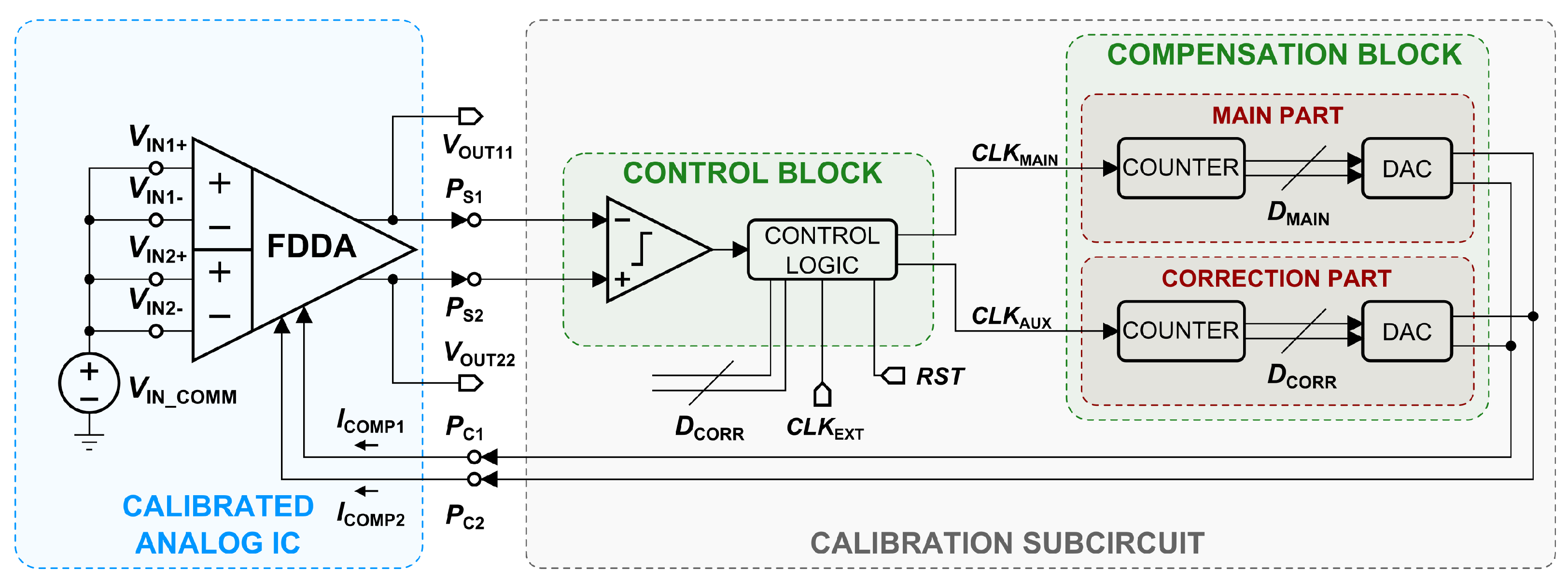
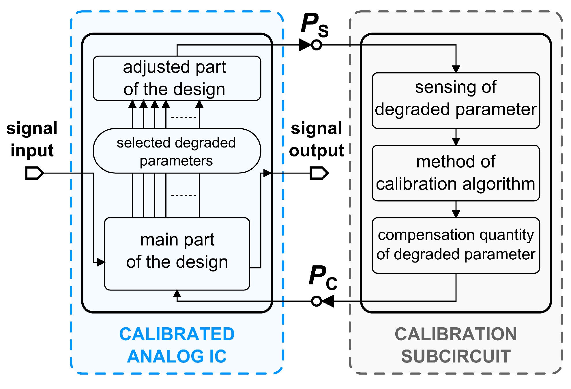
An effective way to provide robustness of analog ICs to PVT variations is additional calibration of specific parameters. Generally, calibration is performed through the compensation of precisely selected IC parameter, a value of which is degraded due to the influence of PVT variations. Such a compensation is realized by employing a calibration subcircuit, as illustrated in
Figure 1. The basic prerequisite for calibration of an analog IC is to adapt its topology by correctly defined sensing port
and compensation port
for compensating the degraded circuit parameter. The sensed value of such a parameter is fed to
port, which basically serves as a control variable for the calibration subcircuit. According to the degree of degradation that represents the key information, the calibration subcircuit brings a certain specific quantity to port
, which compensates the sensed parameter degradation. The primary requirement for the calibration subcircuit is that it does not adversely affect the calibrated analog IC. Additionally, from the low-power requirement point of view, its power consumption should not significantly increase the overall consumption. The area overhead, reliability and efficiency of calibration hardware are other important aspects. Last but not least, the calibration subcircuit itself must be very resistant to PVT variations.
2. Calibration Techniques
Nowadays, there are several techniques for calibrating analog ICs and compensating unwanted effects on their parameters. The superiority of calibration techniques lies in the exact adaptation of calibration subcircuit design to the designer-specified degraded parameter of the tuned circuit. This section offers brief review of existing calibration techniques such as fuse trimming technique (using standard fuses and anti-fuses), chopper stabilization, auto-zero technique, general analog and digital calibrations. Brief comparison of these approaches is given at the end of this section.
Fuse trimming technique consists in multiplying critical CEs in the analog IC. Additional trimming can be realized through the use of standard fuses or the use of anti-fuses on a chip, and both realizations are analogous in application. As for a principle of operation, they can be considered as mutually inverse. Electrical resistance of the fuse after it blows increases approximately a million times. In [
9], an NMOS transistor controlled by a NOR gate is used to blow the fuse. In [
10], the fuse blowing by connecting voltages of 1.5 V and 2 V is shown as illustrative comparison. Fundamental difference between standard fuse and anti-fuse approaches is their initial conductivity. In [
11], an one-time-programmable antifuse (OTPA) implemented in CMOS technology is presented. In this case, the gate oxide of an NMOS transistor serves as a high-impedance element, which could be blown by connecting the necessary value of breakdown voltage
to the specific contacts of the transistor (depending on used type). Within the application, this anti-fuse is used in a 1-bit 3T NMOS memory cell. The work [
12] also introduces anti-fuse based memory, where junction-less gate-all-around nanowire single transistor (1T) is used to demonstrate OTPA.
Chopper stabilization (CS) is primarily used for effective compensation of unwanted input offset voltage
and low-frequency 1/f noise in OPAMPs. In terms of analog IC calibration, this method is classified as dynamic one. The main idea behind CS lays in modulating the useful signal to a sufficiently high frequency, where the influence of input offset voltage and 1/f noise is negligible. This signal is subsequently amplified and demodulated to the original frequency. Modulator/demodulator could be designed by cross-connected MOS transistors or use of CMOS transmission gates [
13,
14,
15]. The CS principle visualized through the spectrum analysis is scrupulously analyzed and presented in [
16], where the CMOS bandgap voltage reference is calibrated using CS and fabricated using high temperature and high pressure CMOS 180 nm technology. In work [
17], CS is used to calibrate
of analog multipliers.
The auto-zero (AZ) technique is based on sampling an unwanted signal and then subtracting the voltage value of a sample from the useful signal. Similar to the CS technique, AZ is very often used to minimize the
of OPAMPs. The principle of AZ is also presented in [
13]. Implementation of AZ could be realized either in analog or digital way [
18]. In [
19], continuous AZ OPAMP able to achieve 2
V
used for light sensing application is discussed. Except the OPAMP
calibration, AZ technique is also applicable for the calibration of voltage comparators [
20]. In [
21], a voltage buffer with the maximum
value of 0.6
V was calibrated using this technique.
Analog calibration approach consists in the individual design of a calibration subcircuit comprising analog circuits. In [
22], analog calibration of the voltage comparator for
calibration is described. The calibration is aimed at the substrate voltage
of input transistors. In [
23], the analog calibration of a dual-mode voltage-controlled oscillator (VCO) is designed. Depending on whether the value of output voltage
is higher or lower than the reference value
, the current source will decrease or increase the tuning current value for the calibrated VCO circuit.
The main idea behind the digital calibration of analog ICs is analog-to-digital conversion of the degraded parameter quantity being sensed, its digital processing and evaluation in order to generate a compensation value, and then perform a reverse digital-to-analog conversion and bring this compensated value to a specific node of analog IC. Again, this calibration method requires an individual approach to a specific application. Similar to analog way, a calibration system designed on a digital principle can be highly versatile. In [
23] (in addition to the analog calibration), the digital calibration is also presented within the dual-mode VCO. In this case, the calibration technique is implemented as a digital-controlled current source, and a comparison between the given calibration approaches (for a specific application) is presented. It was shown that the digital mode of calibration offers higher level of stability and lower consumption. The research presented in [
24] investigates a digitally trimmable 24-GHz low-noise amplifier, which is a part of the microwave receiver system. This trimming approach is based on switched capacitors to the ground. In [
25], one can find a built-in digital self-calibration technique of analog-to-digital converter (ADC) aimed at minimizing the integral nonlinearity.
In
Table 1, the properties of presented calibration techniques for analog ICs are compared. The only static method among the analyzed techniques is fuse trimming (both realizations). Therefore, it is unjustified to discuss signal processing, noise, transmitted bandwidth or the calibration cycle with this technique. Fuse trimming is one-time and irreversible process that requires a non-negligible area overhead. The CS technique offers both sampled and continuous signal processing, which means more application possibilities. In its basic implementation (modulator, demodulator), it is the only calibration technique, where the area of additional circuitry is negligible. However, limitation of the calibrated IC frequency band can be a problem in certain applications. On the other hand, AZ technique does not limit the frequency band of calibrated analog IC, which is a great advantage. However, the work with a useful signal resides in a sampling way only. Digital implementation of AZ also has the option of a low-frequency calibration cycle. CS and AZ techniques are often combined into a very effective calibration system using the advantages of both techniques, however, with considerable area overhead. As for the signal processing and frequency options of the calibration cycle, analog calibration represents an adaptable choice for number of applications. Nevertheless, it suffers from noise robustness and the area overhead that increases significantly with the number and complexity of calibration subcircuits needed for implementation. A common property for CS, AZ (both implementations) and analog calibration is parallel cooperation with the calibrated device.
Compared to other techniques, digital calibration according to the given data offers the most adaptable option in terms of its implementation. It can be designed for once, repeatably, or in parallel cooperation with the calibrated analog IC. The useful signal can be sampled or processed continuously as needed, while it is possible to ensure low noise and at the same time not limit the band of the analog IC. The same applies to the calibration frequency, which can be used as needed. As already mentioned, the entire calibration subcircuit also requires a certain chip area, but considering its advantages, this shortcoming is acceptable. Thus, considering the versatility and all aspects regarding the digital calibration, our research was focused on development, implementation, simulation and experimental evaluation of this technique towards silicon-proved results.
In our previous research, we have developed a new digital calibration system for the
compensation in a bulk-driven variable gain amplifier (VGA) with differential output [
26]. The importance and appropriate topology of the DAC that is directly connected to the calibrated analog circuit was evaluated. In [
27], adverse effects of digital calibration hardware on the VGA performance was investigated through modeling the critical parts of the system. Models of transistors connecting the calibration subcircuit and the analog IC in calibrated and non-calibrated configurations are analyzed. Then, improvement of the digital calibration approach by the use of SAR logic was presented [
28], and modification of the calibration technique towards ping-pong implementation was described in [
29]. Both works comprehensively present design of the system, its physical layout implementation, and bring simulated and measured results.
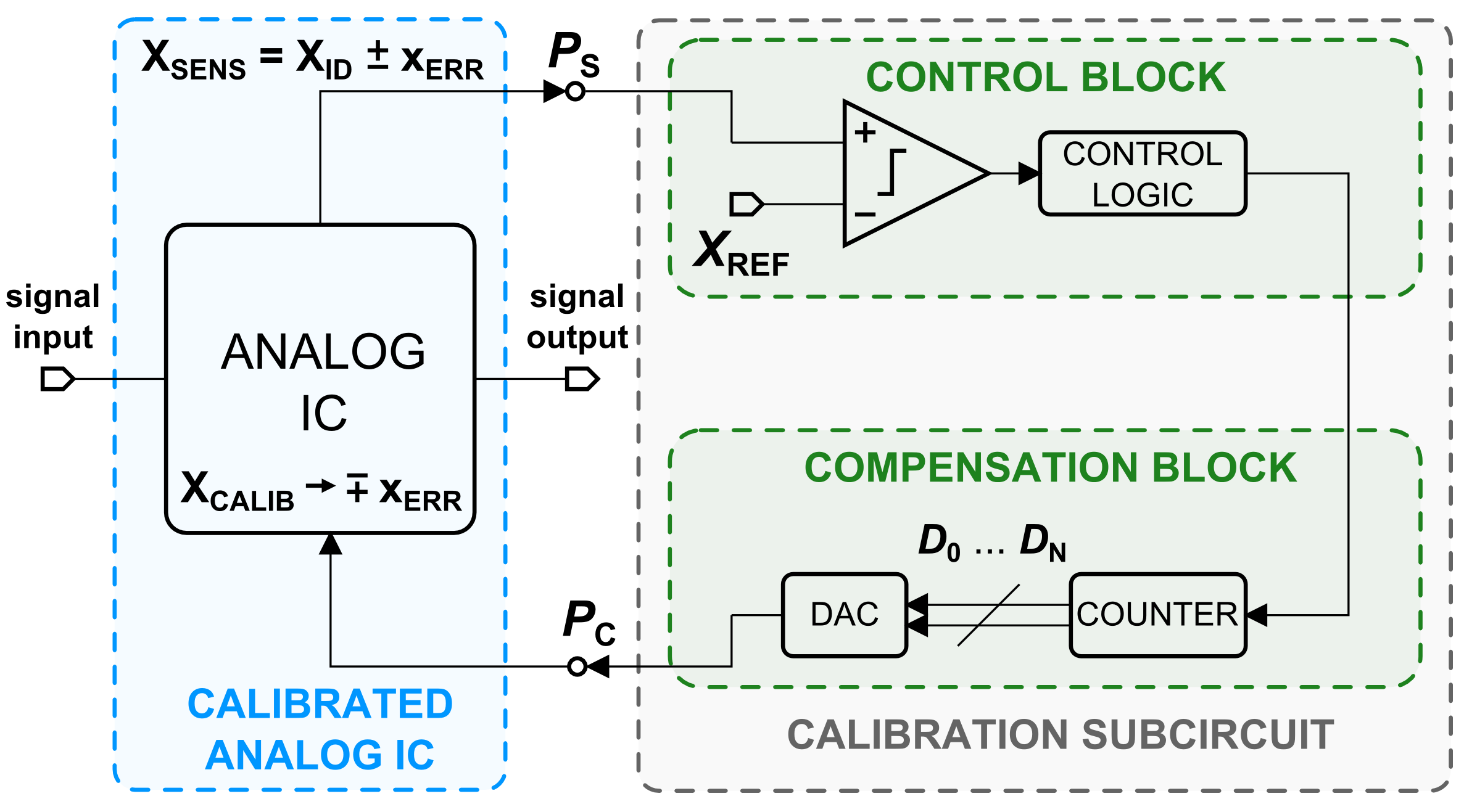
3. Proposed Digital Calibration System
In this work, a new modification of the digital calibration approach to FDDA
compensation was developed. Main block diagram of the digital calibration system used for this purpose is presented in
Figure 2. One can observe that two major parts of the calibration subcircuit are: control and compensation blocks.
Tasks of the control block are to sense the actual value of the specified degraded parameter at port
, evaluate this value, and generate appropriate master signal(s) for the compensation block. This sensed value
can be expressed as follows:
where
represents the ideal value of degraded parameter and
is deviation from the ideal value. Then, the comparator compares the
value to the reference value
(
). The control logic monitors the comparator output and controls the compensation block through a suitable algorithm until the calibration process is finished.
The compensation block consists of a DAC that is drived by a counter. The control signal coming from the control block makes the counter increment its output value that is sent in parallel via
bus (
N means number of bits) to the DAC. The DAC output represents value of the compensated parameter
fed to the analog IC during the calibration cycle. In this case, a very important aspect is synchronization of the whole system, because incrementation of the
value must cause decrementation of
. The resulting value of the compensated parameter
is given by:
where
is the minimum deviation value distinguishable by the calibration subcircuit. At the moment when
, the control logic stops its output signal and the compensated parameter value
is permanently (also during the analog IC application) fed to port
.
3.1. Operation Principle and System Design
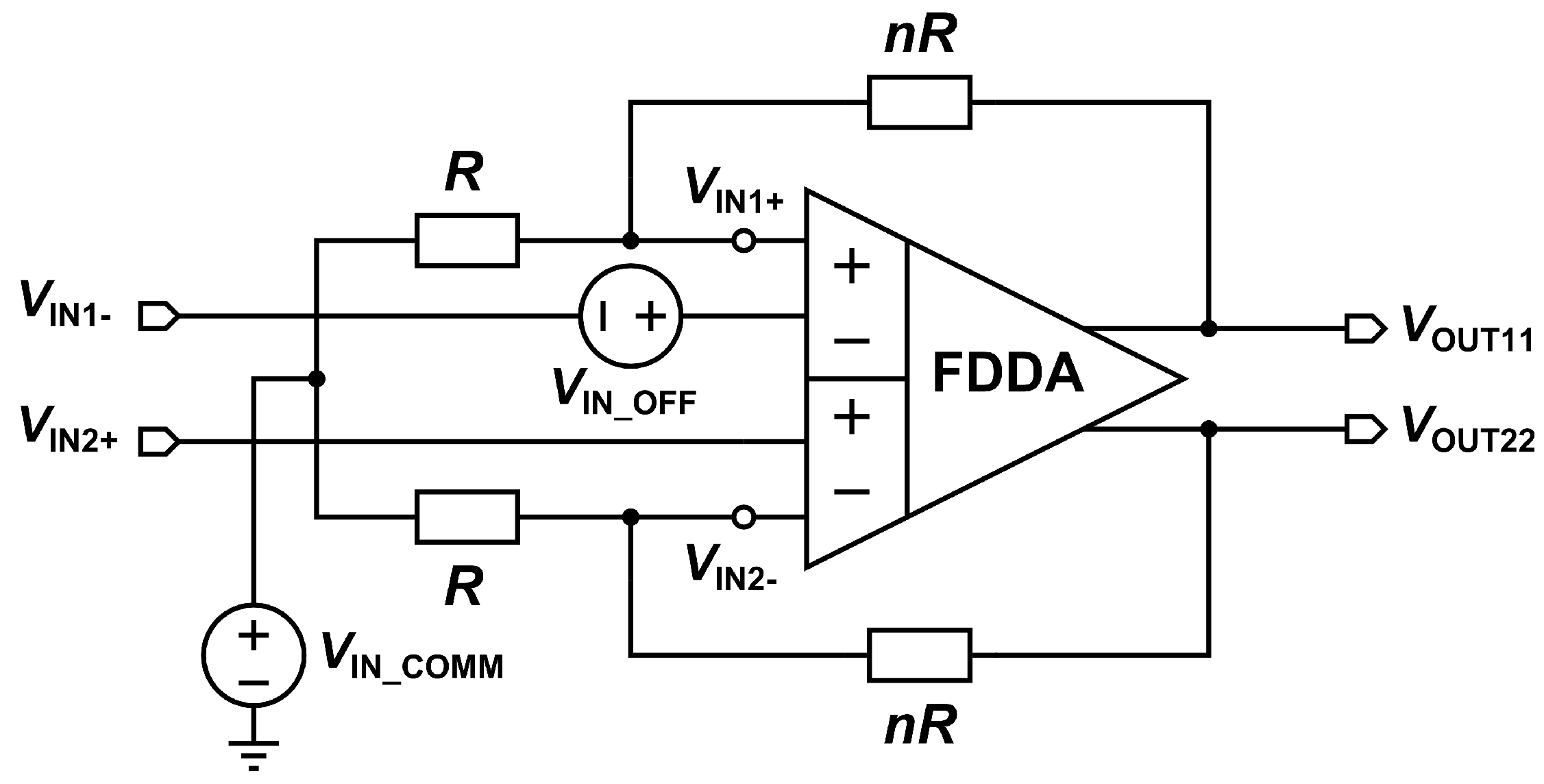
The essence of digital calibration system, in this work, is to compensate
of the FDDA. The whole methodology consists in sensing and evaluation the output offset voltage
. Consequently, based on its value, compensation currents are generated and fed into the input differential pairs. Relation between
and
can be obtained from the following facts. Convenient configuration to detect FDDA
is shown in
Figure 3. It is important to note that
of FDDA was not symmetrical in simulations, and therefore,
= 400 mV means input common DC voltage
= 200 mV.
This topology is based on well-known differential OPAMP offset detection configuration. The great advantage of FDDA circuit is direct connection of the useful signal to the amplifier.
can be provided from the following equation [
26]:
where
is the FDDA close loop gain (ideally
=
n),
and
represent the differential input and output voltage of FDDA, respectively. In this case, when detecting
, all inputs are connected to
potential which means useful signal
= 0 V and
=
. Then, it can be written:
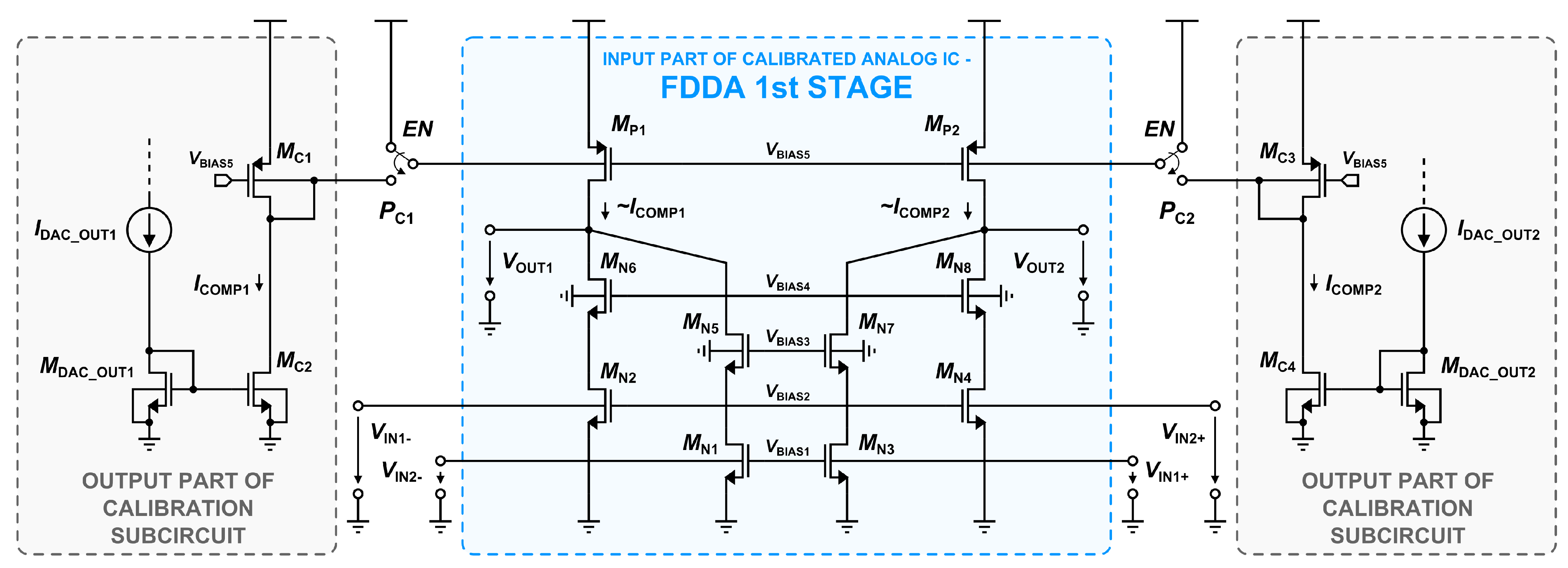
Digital calibration system for the FDDA is depicted in
Figure 4. It can be stated that the whole calibration subcircuit works as a voltage-to-current converter. In this case, the sensing quantity
is differential output signal of the FDDA consisting of two components
and
. Based on this fact, two sensing ports
and
were considered. Similarly, compensation parameter
involves two compensation currents
and
.
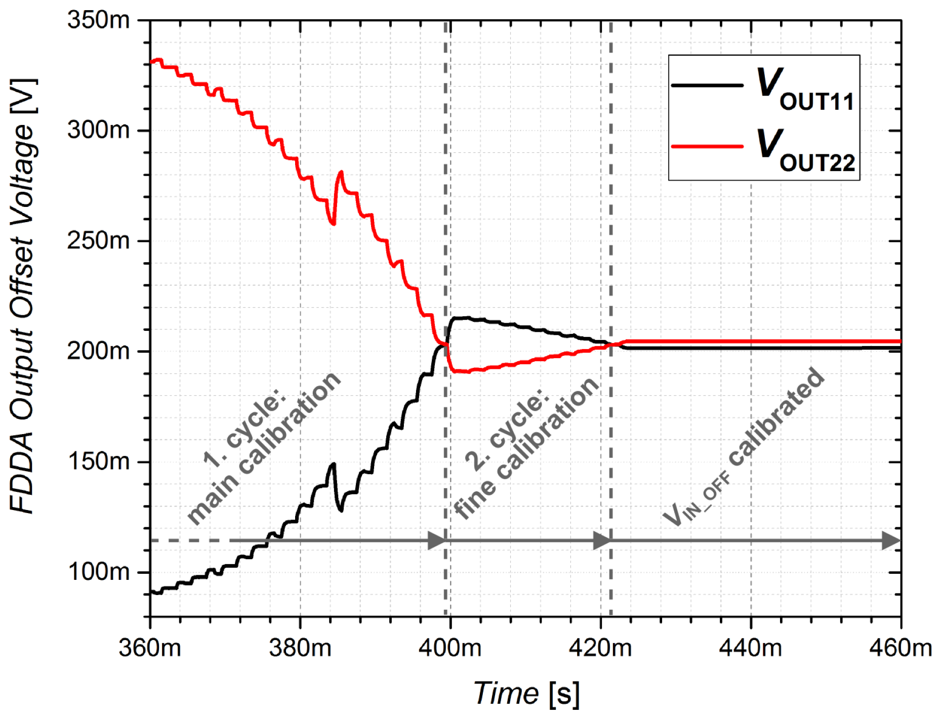
Calibration process takes place in an open loop configuration in two cycles: main calibration cycle and fine (or correction) calibration cycle. This is the reason why compensation block consist of two parts. Result of the calibration algorithm in terms of
is shown in
Figure 5, and explained in detail in the following section.
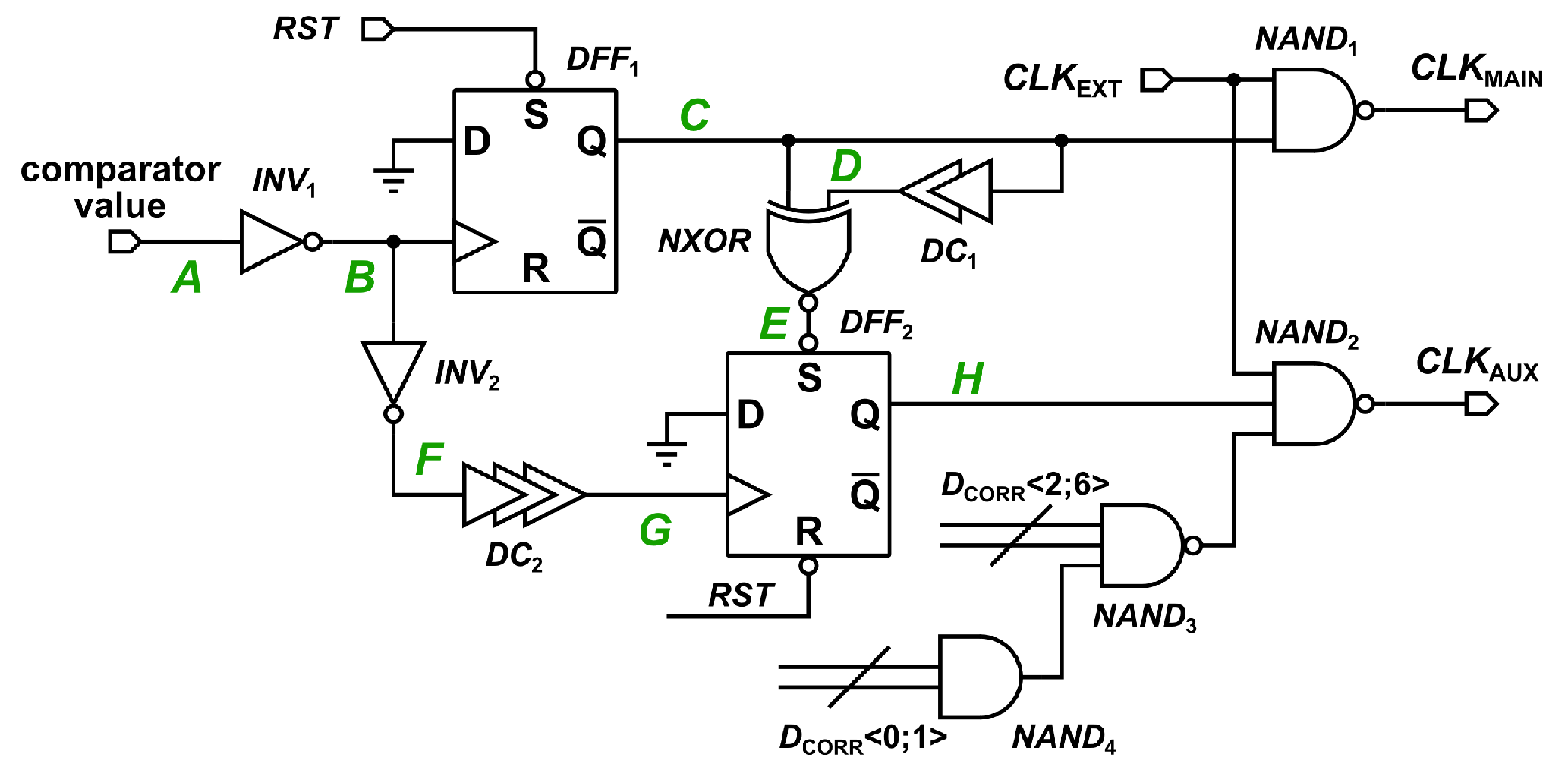
3.1.1. Control Logic: Generating and Signals
With the use of differential output, no external reference for the comparator is needed in this topology since the individual signals
and
are the referencesto each other. In the initial state of non-calibrated FDDA, at the moment when calibration is enabled, the control subcircuit disperses values of
and
(to be explained later). This means that the comparator output acquires the value of logical 1, and the first calibration cycle starts. In
Figure 6, design of the control logic block is shown. All of the signals inside of this block are marked by letters
A–
H and visualized in
Figure 7a during the most important part of the control logic function.
Circuits
and
(signals
C and
H) are initially set to logical 1 and logical 0, respectively, by the external
signal. In the first calibration cycle, signal
B is set to logical 0, so the signal
C is still in logical 1. Through the
gate, control signal
is generated. At the moment when signals
and
reverse their polarities relatively to each other, comparator flips its output value to logical 0. Rising edge of the signal
B changes the logic value of signal
C to logical 0. This means
gate stops the
signal and the main calibration cycle ends. Meanwhile, when signal
C is flipped to logical 0, the delay cell
takes place to generate signal
D for creating short impulse of logical 0 (signal
E) through
gate to set
(signal
H) to logical 1. The length of this impulse is ≈40 ns. This phenomenon can be seen in
Figure 7b, where all crucial signals are zoomed in. At this moment, the second cycle starts and signal
is generated through
gate. To ensure the sequential arrival of signals to
, the delay cell
was used. At the moment, when comparator again flips its output value to logical 1, signal
flips signal
H to logical 0 and
is stopped by
gate.
3.1.2. Digital-to-Analog Conversion
Special emphasis must be paid to the DAC design, since it is a circuit directly connected to the calibrated analog IC. The task of the calibration subcircuit is to find the most appropriate digital values for DAC circuits that will give the best result of the compensated parameter. If it was theoretically possible to achieve an ideal output value of the DAC with infinite resolution, the value of
from Equation (
3) would be zero. The converter resolution creates an error into this process, which corresponds to
value after calibration. From mathematical point of view, any value higher than ideal represents over-compensation, and any value lower, on the contrary, under-compensation [
13].
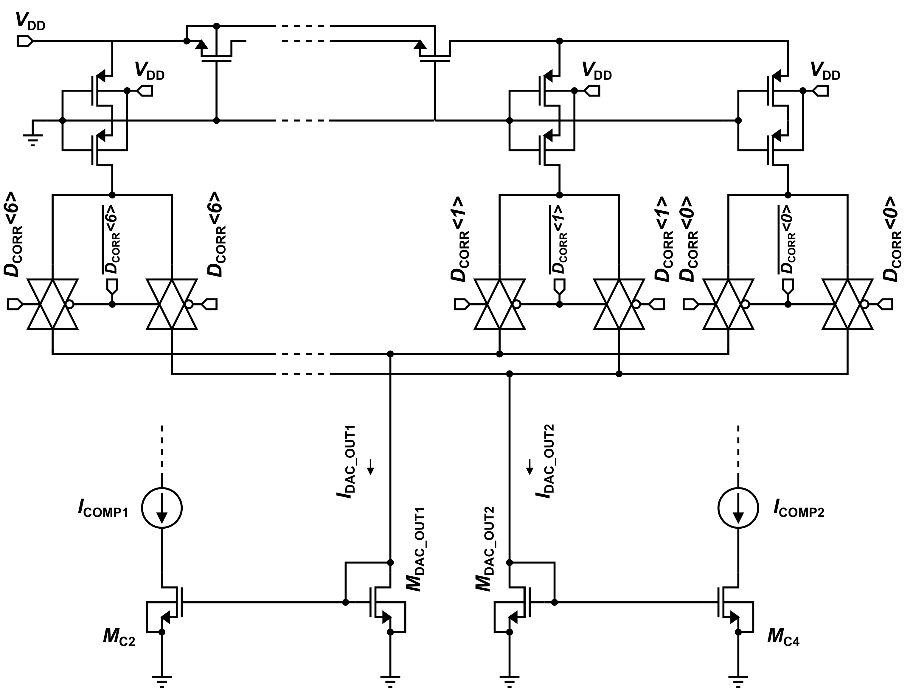
Design of the DAC circuits is realized as an M/2M network [
13]. The R/2R network resistors are replaced by MOS transistors, which analogously work as pseudo-resistors with equivalent resistance. The M/2M network is more practical solution in terms of overall circuit area considered in integrated design. The DAC circuits used for main calibration and fine calibration have resolution of 10 bits and 7 bits, respectively. In the main part of calibration subcircuit (1. cycle), a DAC with a larger step of generating compensation currents is designed compared to the DAC in correction part (2. cycle), which is used for fine tuning. The topology of 7-bit M/2M DAC is shown in
Figure 8. Transistors within the network are switched by transmission gates (T-gates), which are controlled by signals of
parallel buses (
and
). In addition to generating
signals, counters also generate their negations
. Since both types of these signals are used when switching the T-gates, output current
will always be generated on the basis of the opposite digital code compared to
current. At the beginning of calibration process, current corresponding to the full-scale range of the converter
is mirrored into the current branch
, which gradually decreases, and the current corresponding to an ideally zero value
is mirrored into the branch
, which gradually increases. Based on this fact, the branches
and
are dispersed in the manner described above. The effect of connecting the calibration circuit to the FDDA is analyzed in the following section based on critical transistors modeling.
4. Undesired Effects of Digital Calibration System for FDDA
Inteconnection of the DAC output part with the input differential pairs of FDDA is shown in
Figure 9. This connection is controlled by an external enable signal
that connects the substrate electrodes of transistors
and
at the branch belonging to
, and
and
at the branch belonging to
. By turning on
switches at the compensation ports
and
, bulk-driven current mirrors are created, through which the compensation currents are mirrored into the corresponding branches. As for the influence of this connection, the output impedance
of one half of the symmetrical input pairs in the calibrated and non-calibrated FDDA configuration was analyzed.
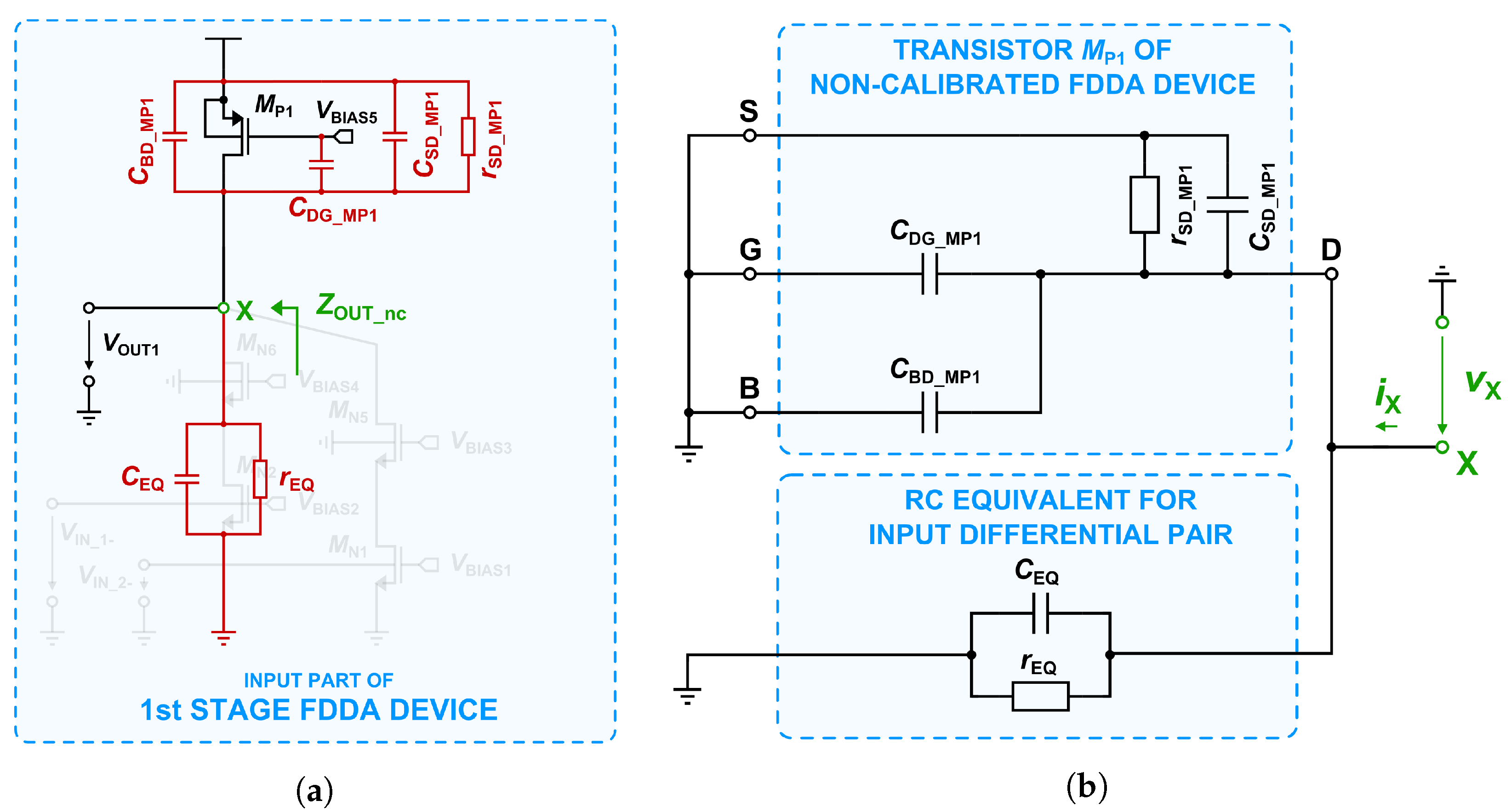
In
Figure 10, the non-calibrated FDDA configuration modeling is shown. In this case, the input differential pair is substituted by an equivalent resistance
and capacitance
. Not all parasitic capacitances are marked here for transistor
because of the specific connection of the given transistor.
Figure 10b shows a model of the circuit situation depicted in
Figure 10a. As it can be seen, only parasitic capacities
,
,
and resistance
stand out in this model. In general, for
in node
X, the equation takes place:
where
and
are voltage and current in the node X. For the output impedance in node
X of non-calibrated FDDA configuration
, the equation applies:
where all of the symbols are mentioned in
Figure 10. To simplify this relation, the following approximation can be used:
Then, output impedance
can be derived as:
Based on Equation (
11), it can be concluded that among the listed elements,
have the greatest influence on
in this case. Another situation is depicted in
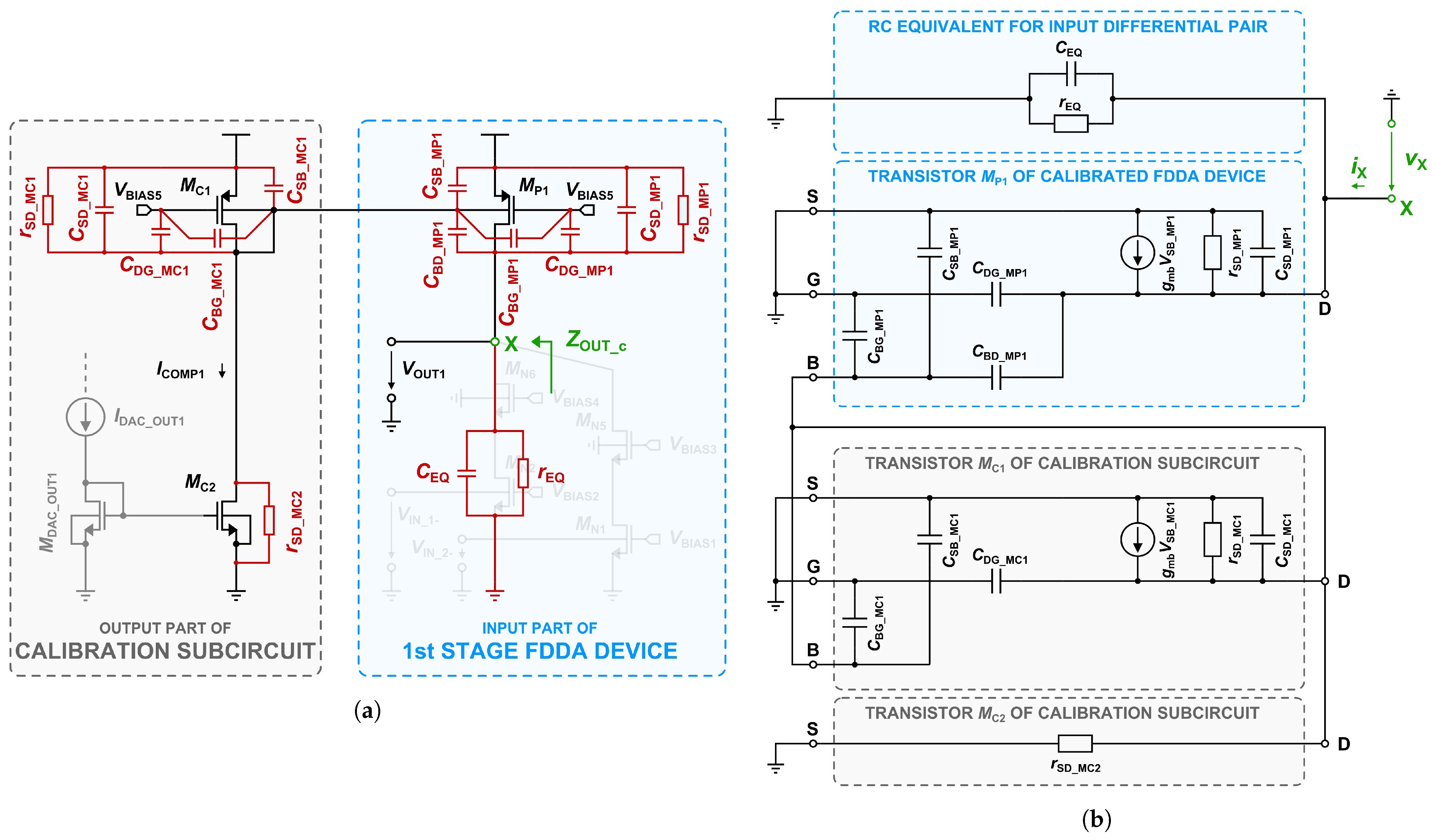
Figure 11, where calibrated FDDA configuration modeling is shown. In terms of transistor
, two more parasitic capacities
and
are considered here because of the bulk
and
connection. Marked parasitic capacities of transistor
are similarly based on its particular circuit connection (mirror transistor). Transistor
is modeled only by its output resistance
.
Figure 11b shows a model of the system situation depicted in
Figure 11a. Calibrated FDDA output impedance
could be described using
as follows:
where for
,
and
applies:
and where
is a sum of all parasitic capacitances of
transistor:
All of the other symbols used are marked in
Figure 11. Compared to
, the
impedance function also contains the substrate conductivity of both transistors (
and
), which can significantly influence this impedance. It is also possible to observe the presence of the second pole. For the proper design of the calibration subcircuit connection, dimensions of the transistors
,
,
and
are crucial, so as not to affect the frequency and phase responses in calibrated FDDA configuration [
30].
6. Simulation Results
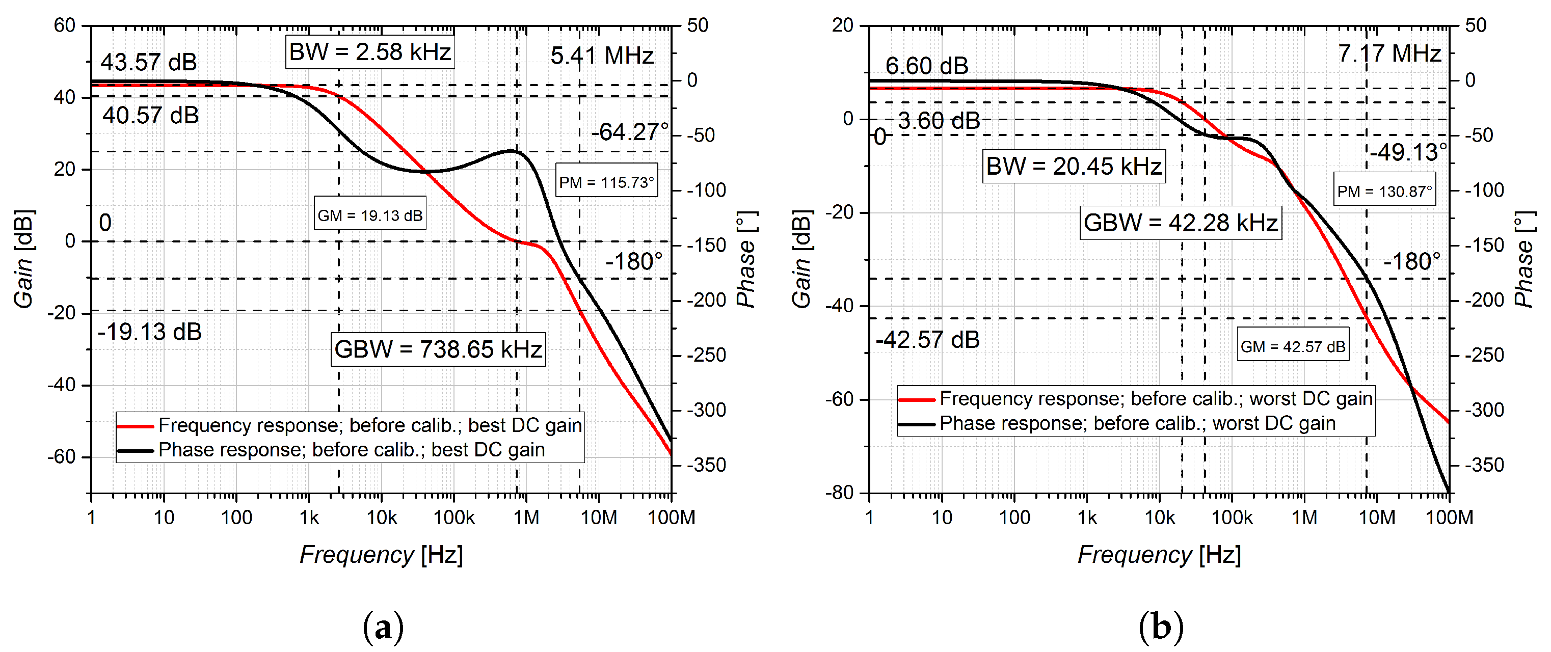
This section presents results of simulations in two groups data obtained before and after FDDA calibration using Monte Carlo (MC) analysis. In
Figure 13, the best case (BC) and worst case (WC) of non-calibrated FDDA frequency response in terms of DC gain are shown. The BC of
(
Figure 13a) was reached with the value of 43.57 dB. In this case, bandwidth (BW) 2.58 kHz, gainbandwidth (GBW) value of 738.65 kHz, gain margin (GM) of 19.13 dB and phase margin (PM) of 115.73
were reached. In the WC of frequency response (
Figure 13b),
of extremely low value 6.60 dB was achieved due to the random variance of technological process and device mismatch. As for other parameters,
= 20.45 kHz,
= 42.28 kHz,
= 42.57 dB and
= 130.87
were achieved.
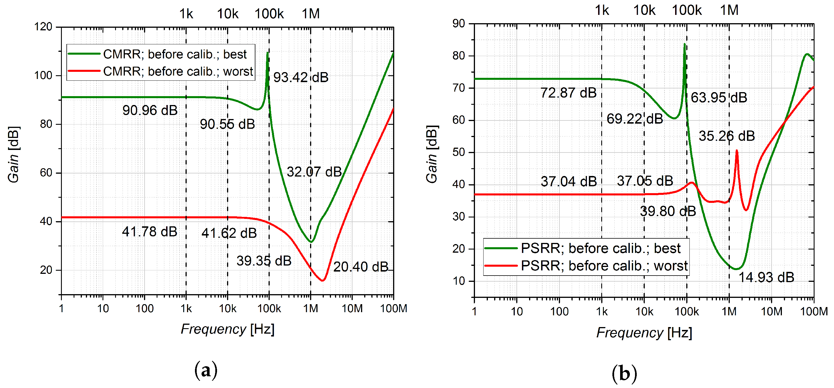
Figure 14a,b show CMRR and PSRR parameters of non-calibrated FDDA, respectively. Selected values at frequencies 1 kHz, 10 kHz, 100 kHz and 1 MHz are marked. In the BC of CMRR parameter, values of 90.96 dB @1 kHz, 90.56 dB @10 kHz, 93.42 dB @100 kHz were achieved, while @1 MHz the value dropped to 32.07 dB. In the WC of CMRR, the curve has similar shape except the dropped value in relative point of view. In this case, values of 41.78 dB @1 kHz, 41.62 dB @10 kHz, 39.35 dB @100 kHz was reached, while @1 MHz the CMRR value dropped to 20.40 dB. In the BC of PSRR, values of 72.87 dB @1 kHz, 69.22 dB @10 kHz, 63.95 dB @100 kHz were obtained, while @1 MHz the value again dropped to 14.93 dB. In the WC of PSRR before calibration, the curve is relatively constant within the 1 MHz band. PSRR values of 37.04 dB @1 kHz, 37.05 dB @10 kHz, 39.80 dB @100 kHz and 35.26 dB @1 MHz were reached.
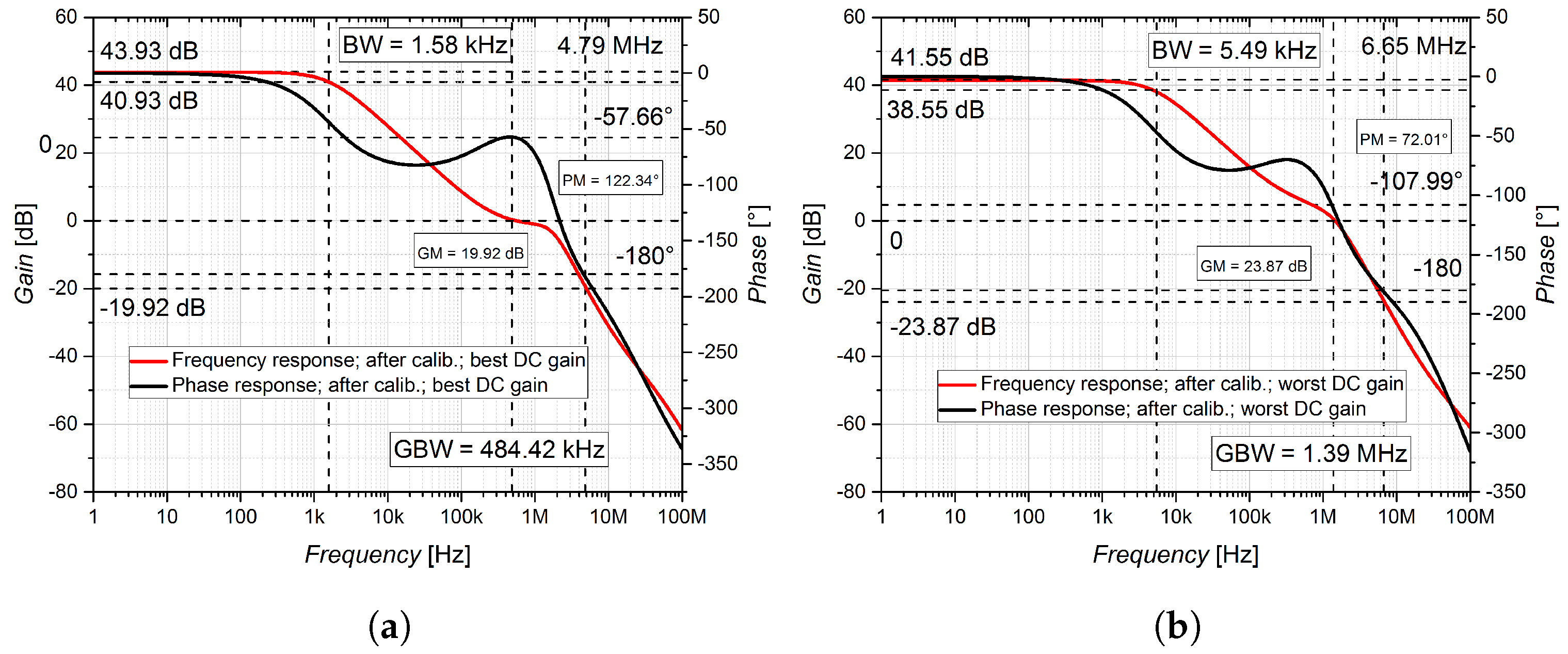
Figure 15a shows BC and WC of frequency response after FDDA calibration. In the BC (
Figure 15b),
= 43.93 dB is almost identical with the value reached for non-calibrated FDDA circuit. On the other hand, the change occurred within the
= 1.58 kHz and
= 484.42 kHz. Also
and
have similar values 19.92 dB and
in comparison to non-calibrated configuration. A considerable improvement in the WC (
Figure 15b) can be observed compared to the non-calibrated version of FDDA. The value of
= 41.55 dB was reached here (compared to 6.60 dB). Also values
= 5.49 kHz,
= 1.39 MHz,
= 23.87 dB and
=
were obtained.
Figure 16 shows BC and WC of CMRR and PSRR parameters after FDDA calibration. As for the CMRR parameter (
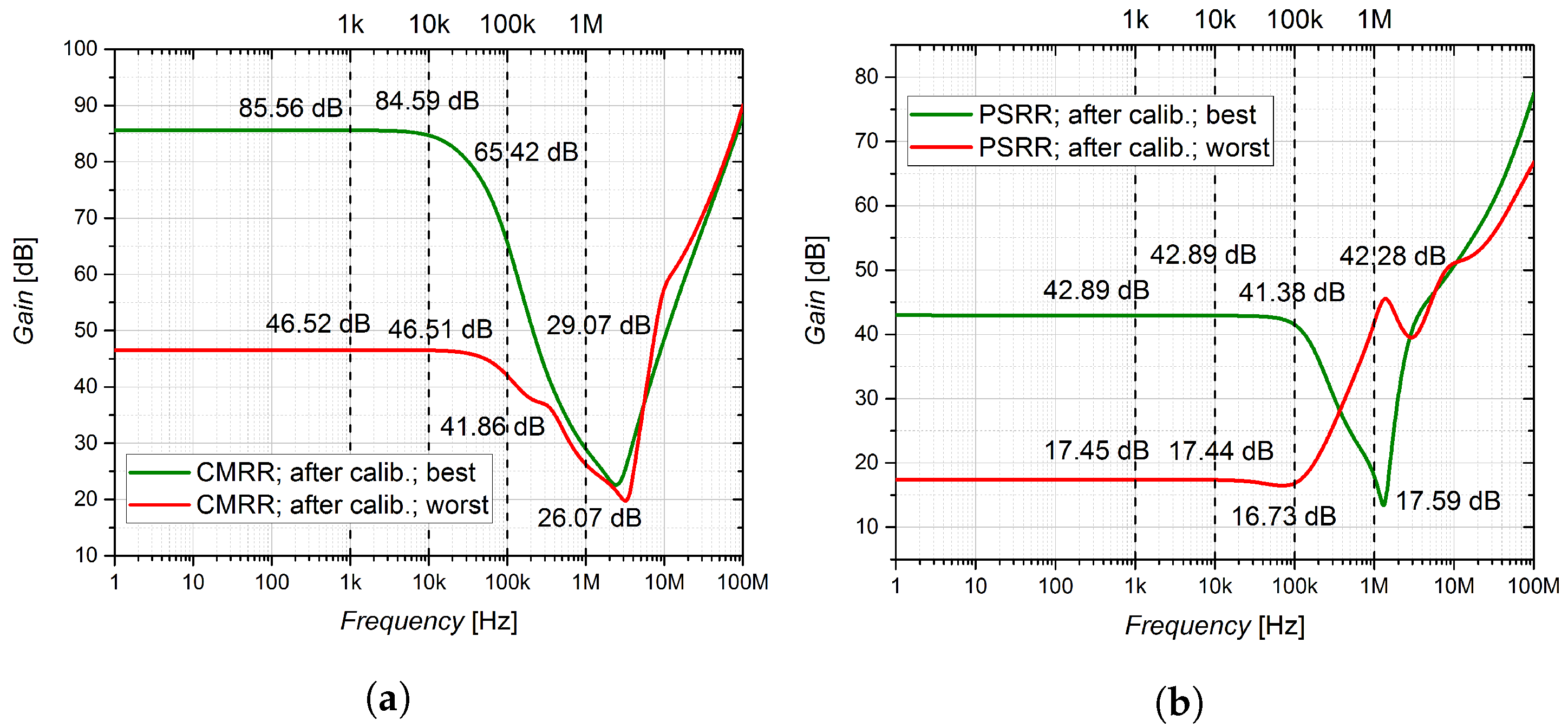
Figure 16a) in the BC, we can state a certain deterioration at all frequencies, e.g. @1 kHz it dropped from the value of 90.96 dB to 85.56 dB. On the other hand, in the WC, an improvement was achieved at all frequencies, e.g. @1 kHz from the value of 41.78 dB to the value of 46.52 dB. In terms of PSRR parameter (
Figure 16b), in simulations we can note the deterioration of this parameter at almost all frequencies again. The value of PSRR @1 kHz represented 72.87 dB in the BC before calibration, while after calibration, this value dropped to 42.89 dB. The WC situation values are very similar with before calibration @1 kHz, where the worst value is equal to 37.04 dB, while after calibration this value dropped to 17.45 dB. Similar decline in values are also @10 kHz and @100 kHz. The only improvement in the case of the PSRR parameter was simulated at @1 MHz, where before calibration in the BC this value is equal to 14.93 dB, while after calibration it rose to 17.59 dB. And the same was true in the WC, where the value before calibration was 35.26 dB, while after calibration, the value is 42.28 dB. This deterioration (or improvement at high frequencies) can be caused by the direct connection of DAC to the input differential pair of FDDA. Through this connection, noise components of the signal can leak from the supply voltage to FDDA.
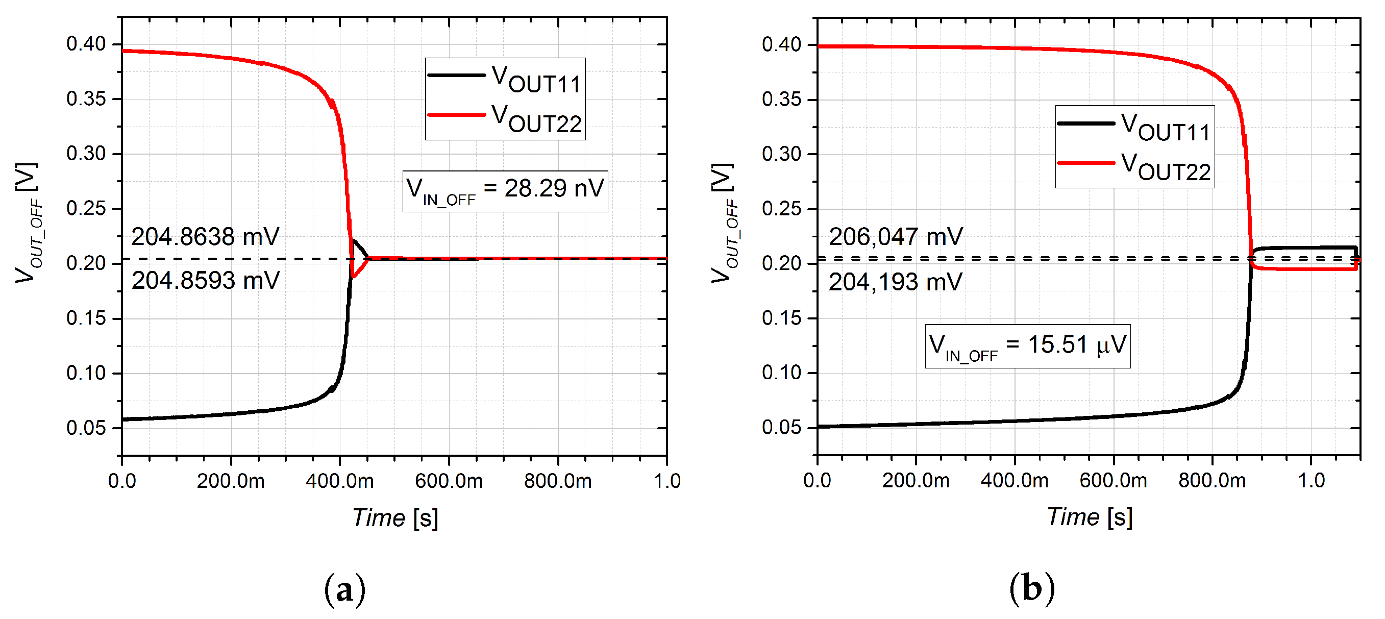
In
Figure 17, the BC (
Figure 17a) and WC (
Figure 17b) of obtained
through the zeroing
are shown. In the BC and WC,
= 28.29 nV and
= 15.51
were reached, respectively.
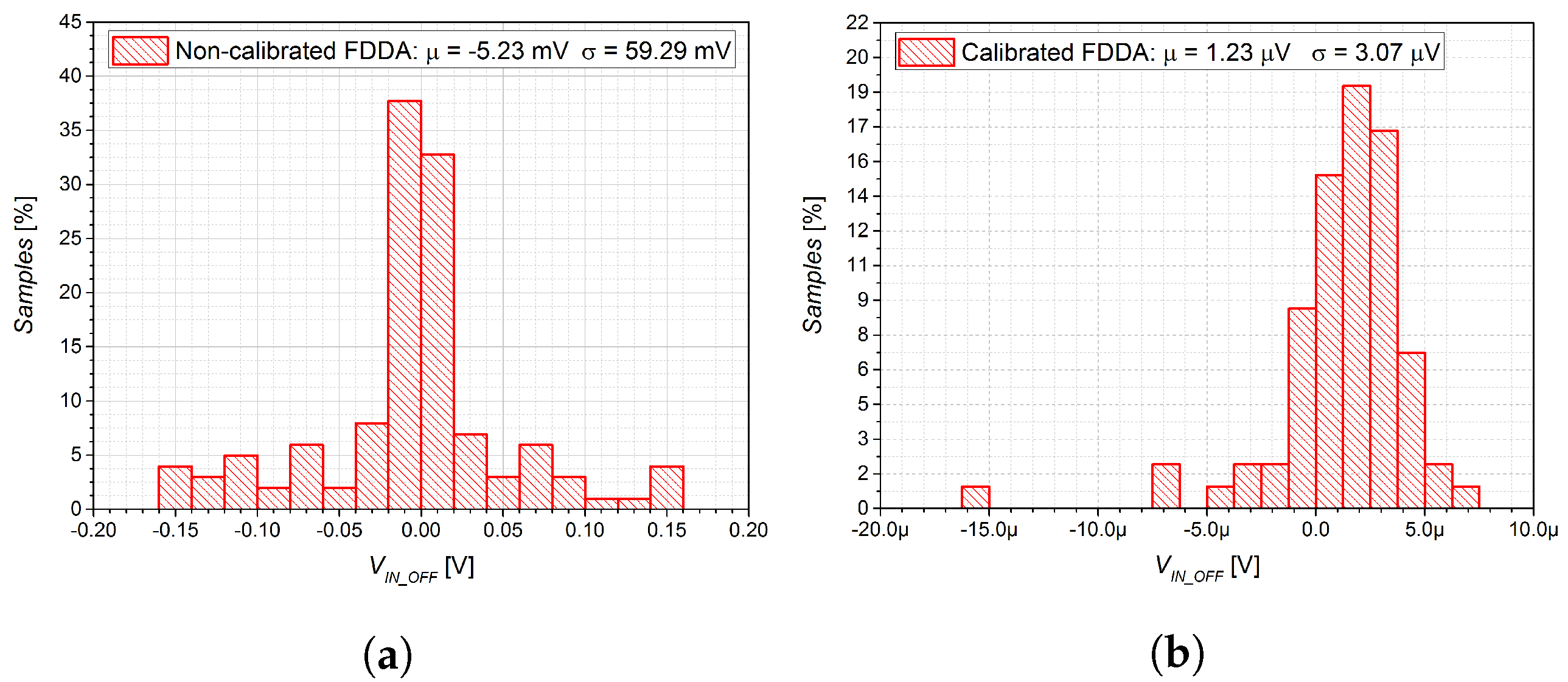
Figure 18 shows obtained histograms of
for non-calibrated and calibrated FDDA. In non-calibrated configuration (
Figure 18a), the mean value
=
mV and standard deviation
= 59.29 mV.
histogram of calibrated FDDA (
Figure 18b) shows the improved values compared to non-calibrated FDDA, where the mean value
and standard deviation
were achieved.
7. Measurement Results
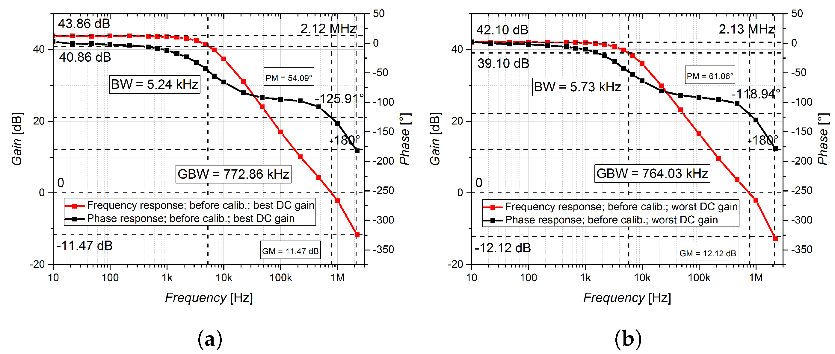
In this section, measured results of the implemented digital calibration system are presented, classified similarly to simulations. The BC and WC of the measured frequency response of FDDA before calibration in terms of DC gain
are shown in
Figure 19. The BC (
Figure 19a) exhibits the following parameters:
= 43.86 dB,
= 5.24 kHz,
= 772.86 kHz,
= 11.47 dB and
=
. In the WC (
Figure 19b)
= 42.10 dB,
= 5.73 kHz,
= 764.03 kHz,
= 12.12 dB and
=
were measured.
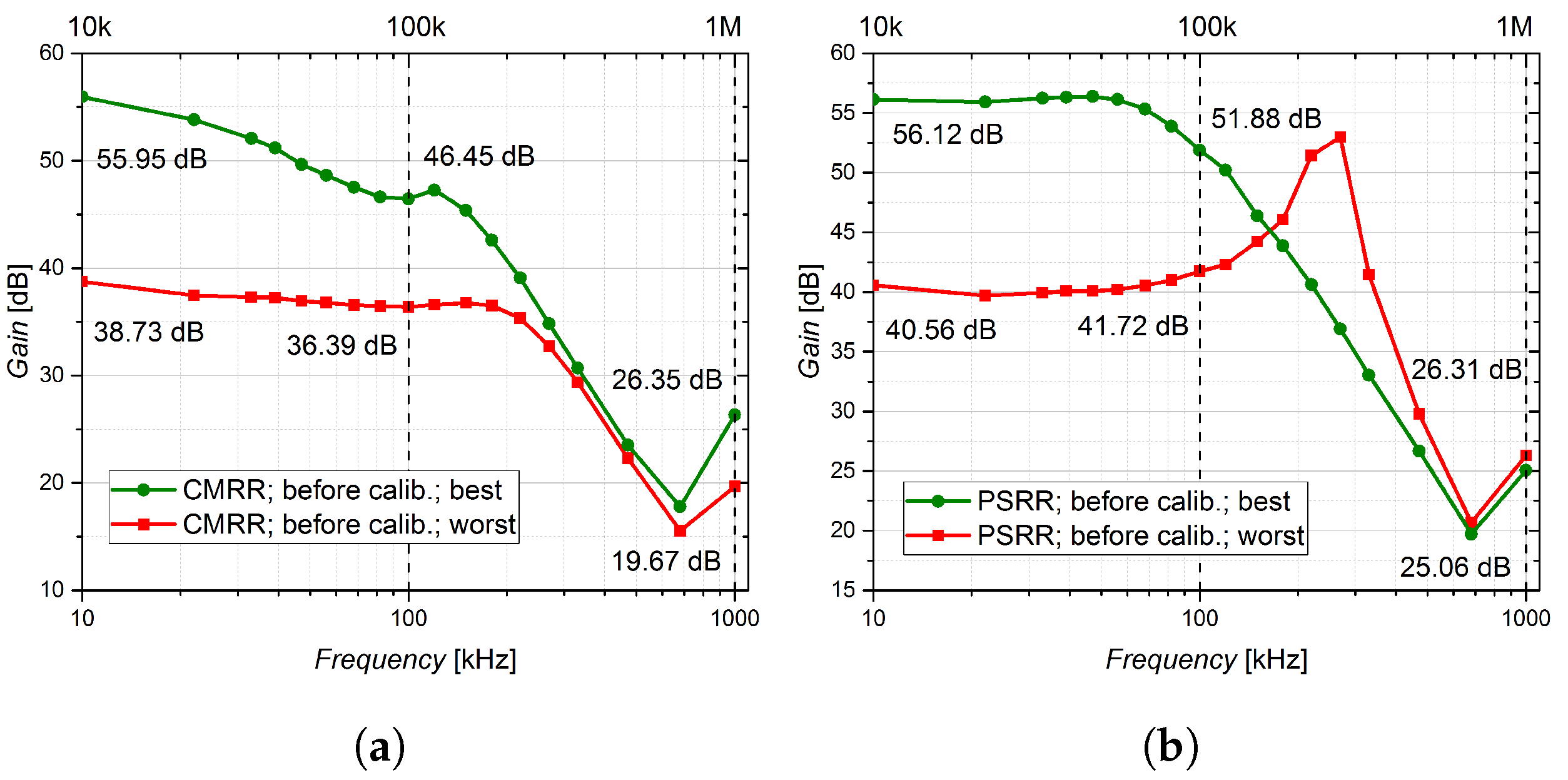
Figure 20 shows evaluated CMRR (
Figure 20a) and PSRR (
Figure 20b) parameters of FDDA before calibration. In this case, selected values at frequencies 10 kHz, 100 kHz and 1 MHz are marked. The BC of CMRR curve has a decreasing tendency, while 55.95 dB @ 10 kHz, 46.45 dB @ 100 kHz and 26.35 dB @ 1 MHz were reported. CMRR in the WC decreases more slowly but with lower initial values of 38.73 dB @ 10 kHz, 36.39 dB @ 100 kHz and 19.67 dB @ 1 MHz. PSRR parameter disposes a relatively constant value up to frequency ≈70 kHz in both cases. In the BC, PSRR values of 56.12 dB @ 10 kHz, 51.88 dB @ 100 kHz are reached, and then it drops to 25.06 dB @ 1 MHz. In the WC, the PSRR value rises within the range ≈70–120 kHz, 40.56 dB @ 10 kHZ, 41.72 dB @ 100 kHz and then, it drops sharply to the value of 26.31 dB @ 1 MHz.
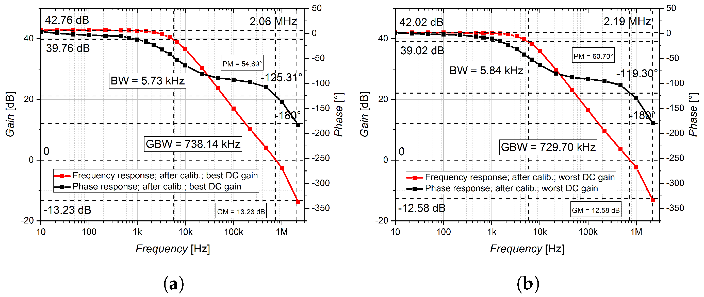
The BC and WC of frequency responses after FDDA calibration are shown in
Figure 21. In both cases, almost all parameters are practically indistinguishable to non-calibrated reached values. In the BC (
Figure 21a),
= 42.76 dB,
= 5.73 kHz,
reaches 738.14 kHz,
and
are equal to 13.23 dB and
, respectively. Similarly, in the WC of frequency response (
Figure 21b),
= 42.02 dB,
and
reach values of 5.84 kHz and 729.70 kHz, respectively, and
and
values of 12.58 dB and
were achieved, respectively.
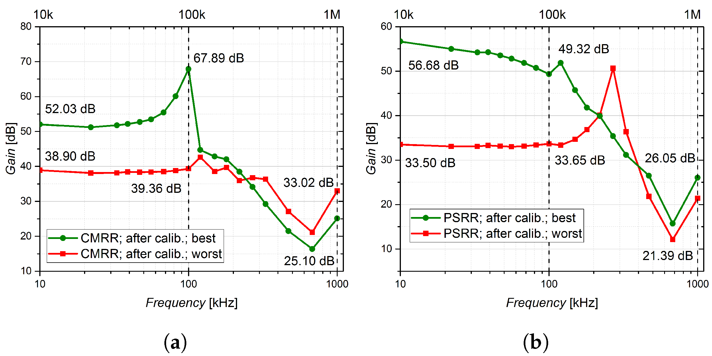
In
Figure 22, the CMRR and PSRR parameters after FDDA calibration are depicted. It can be observed in CMRR parameter (
Figure 22a) that the BC-curve has changed its downward tendency to rise up to ≈100 kHz, where the values 52.03 dB @ 10 kHz, 67.89 dB @ 100 kHz and 25.10 dB @ 1 MHz were obtained. As for the WC of CMRR, the curve shape is very similar to the non-calibrated configuration but at higher values at all frequencies were measured: 38.90 dB @ 10 kHz, 39.36 dB @ 100 kHz and 33.02 dB @ 1 MHz. The PSRR parameter (
Figure 22b) of the calibrated FDDA is, in the BC, almost identical with non-calibrated configuration with the following values 56.68 dB @ 10 kHz, 49.32 dB @ 100 kHz and 26.05 dB @ 1 MHz. Similarly, the shape of the WC-curve is pretty similar to the one of non-calibrated FDDA, however, it lays at lower gain values: 33.50 dB @ 10 kHz, 33.65 dB @ 100 kHz and 21.39 dB @ 1 MHz.
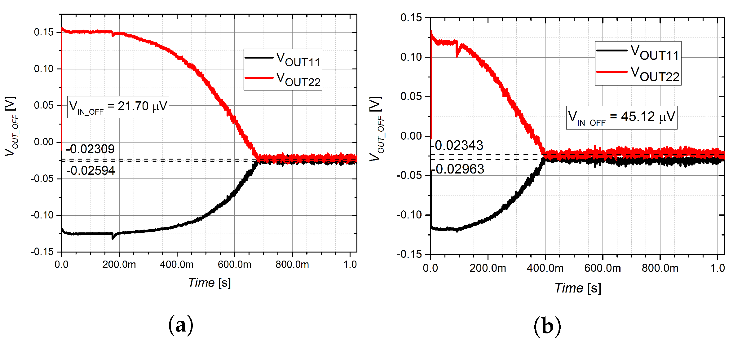
Figure 23 shows the measured calibration effect on
in real time. The BC value is
= 21.70
, while in the WC,
value of 45.12
was obtained.
In
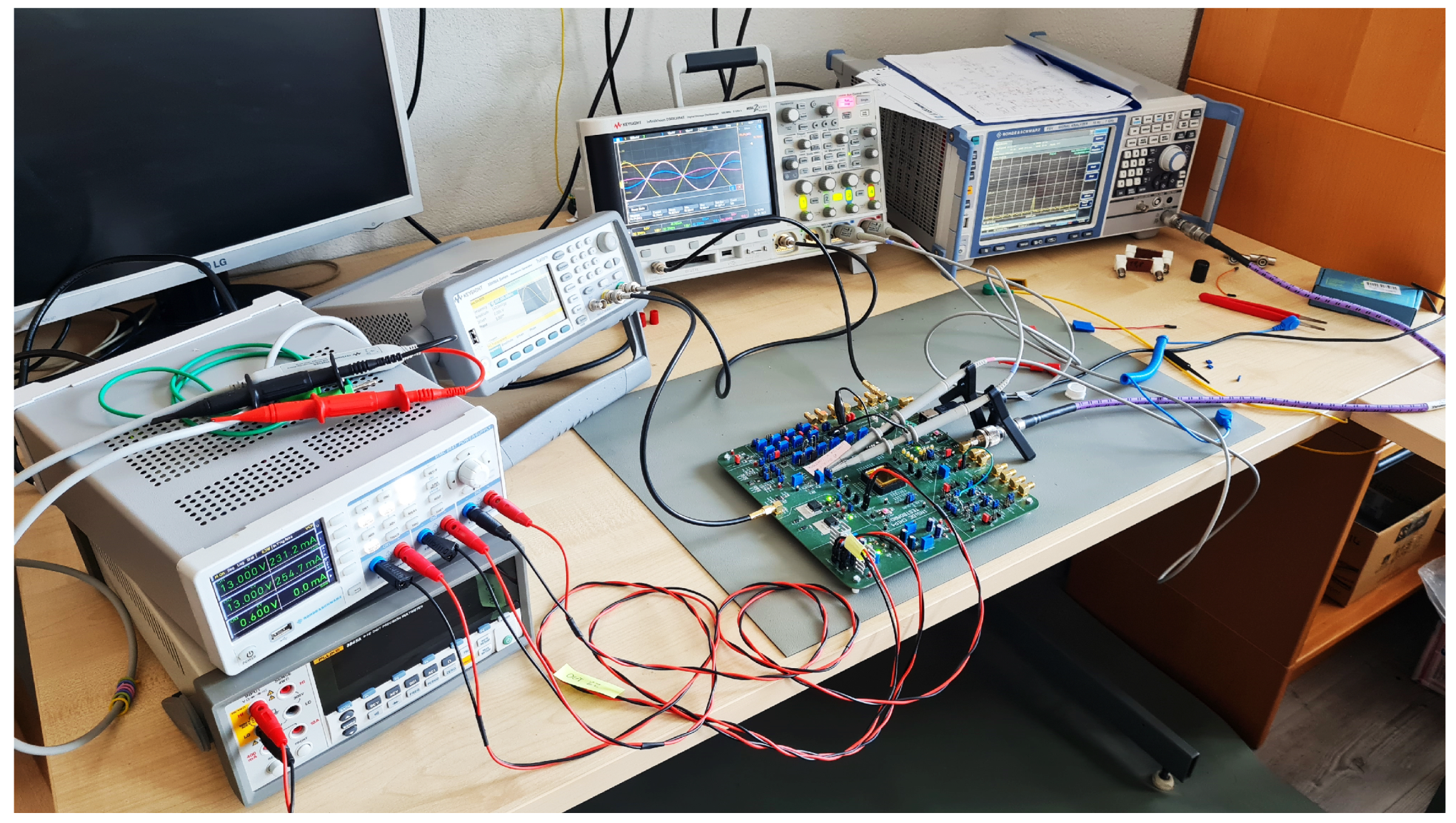
Figure 24, a photography of the evaluation environment including a measurement PCB developed for chip measurements is shown.
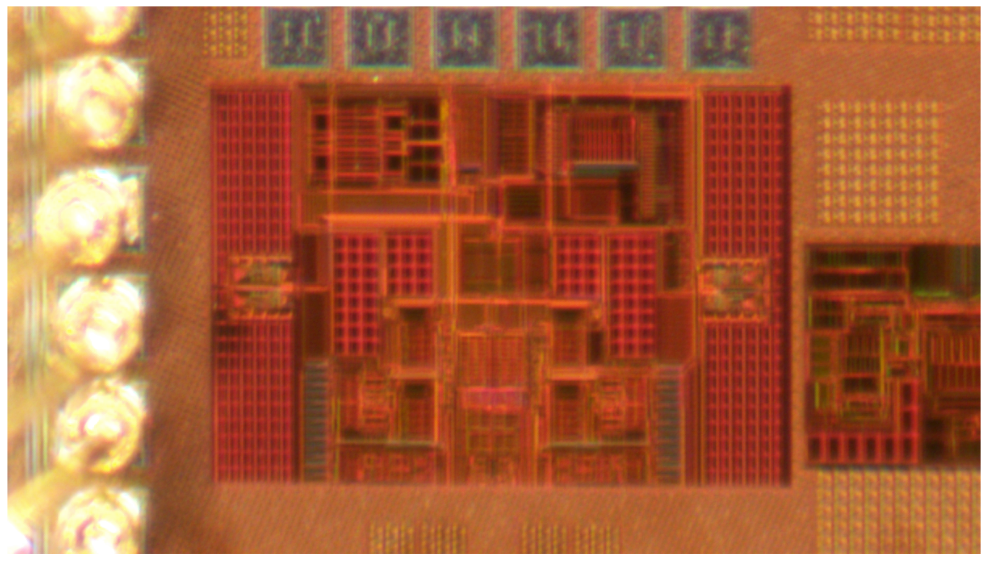
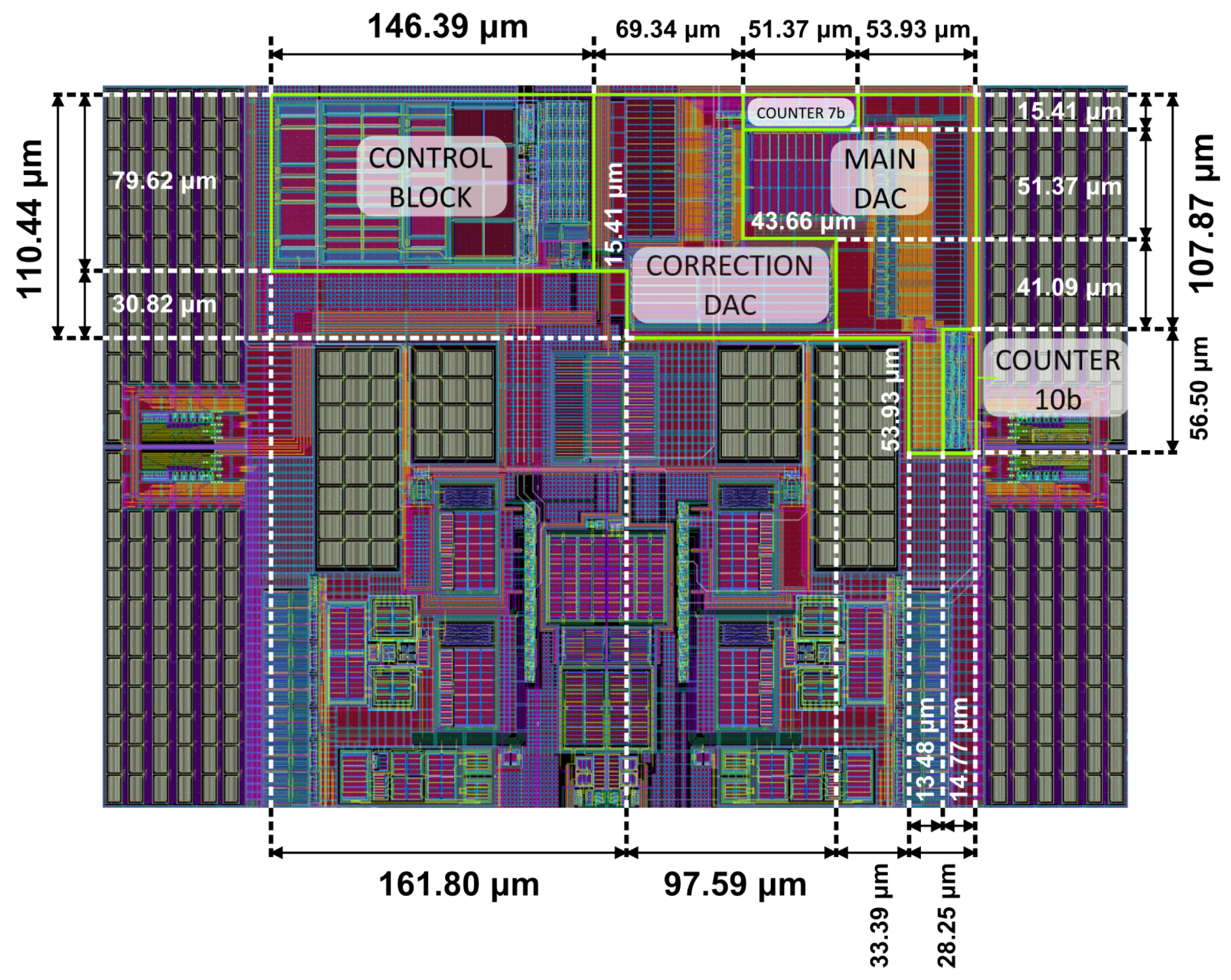
Figure 25 shows under-microscope photography of implemented FDDA with the entire digital calibration system, and bonding wires on the left side of this picture. One can observe that it corresponds with layout exported from the design software environment (
Figure 12).
8. Results Comparison & Discussion
The overall comparison of simulated and measured results of the digital calibration system is presented in
Table 3. Based on this comparison, it can be concluded that all the assumptions obtained by simulations have been confirmed experimentally. In terms of the measured FDDA frequency response after calibration, very similar parameter values were achieved in comparison before calibration,
in range of 42.02–42.76 dB,
in range of 5.73–5.84 kHz and
in range of 729.70–738.14 kHz. The same applies for reached
in range of 12.58–13.23 dB and
obtained in range of 54.69–61.70
. It can be stated the calibration subircuit does not affect the frequency properties of the FDDA. It is a consequence of the correct transistors dimensions design at the DAC output and bulk-driven current mirrors. The simulated values of CMRR parmeter were degraded in BCs after calibration, but improved in the WCs after calibration. The measurement values of CMRR were improved in generall, because WC boundary was shifted from the range of 19.67–38.73 dB to the range of 33.02–39.36 dB at selected frequencies.
The degradation of PSRR parameter reflects the diminution of the WC boundary from the range of 26.31–41.72 dB to the range of 21.39–33.65 dB at selected frequencies after FDDA calibration. As already mentioned, this PSRR degradation was caused by the connection of DAC output transistors and bulk-driven current mirror to the input differential pair. Measurement results proved that afterr FDDA calibration, was improved from the value of −0.4416 mV to the value of 21.70 in the BC, and from −3.8471 mV to 45.12 in the WC scenario.
Establishment of representative figure of merit (FOM) is hindered by limited results provided by other works. These are aimed mainly on application, where OPAMP calibration is used. Therefore, the performance of the developed calibration method is of the secondary interest. FOM is built in relative (
) and absolute (
) perspectives, as follows:
where
is scaling constant,
is reached
,
and
are of calibration hardware and IC under calibration, respectively, and
and
are power consumption of calibration hardware and calibrated IC, respectively.
The
quantifies the proportion of calibration related hardware to calibrated amplifier in terms of area and power consumption demands. The
represents these quantities of calibration hardware in the absolute manner. Both versions are directly proportional to residual input referred offset of amplifier after the calibration is carried out. Furthermore, the scaling constants are used to improve clarity of results and set as
=
and
=
.
Table 4 compares the key parameter results of our work compared to the other state of the art works.


 ,
, 


