Article

Designing an Electro-Optical Tunable Racetrack Microring Resonator on a Diamond–Lithium Niobate Thin-Film Hybrid Platform

1
School of Optoelectronic Engineering, Xi’an Technological University, Xi’an 710021, China
2
College of New Materials and New Energies, Shenzhen Technology University, Shenzhen 518118, China
*
Author to whom correspondence should be addressed.
Electronics 2023, 12(22), 4616; https://doi.org/10.3390/electronics12224616
Submission received: 7 October 2023 / Revised: 3 November 2023 / Accepted: 9 November 2023 / Published: 11 November 2023
(This article belongs to the Section Optoelectronics)

Abstract

:
This study proposes and simulates a numerical analysis of a diamond racetrack microring resonator on a lithium niobate thin film, operating at a 1.55 µm wavelength. The single-mode conditions, transmission losses, and waveguide dispersions are systematically examined. The microring resonator’s radius and gap size are computed and optimized. The designed racetrack microring resonator exhibits a high quality factor (Q-factor) and a high coupling efficiency of approximately 6100 and 95%, respectively, for the transverse TE mode in the C-band. This study achieves a resonant tunability of 1.84 pm/V near the 1.55 μm wavelength by harnessing the electro-optical effect of lithium niobate.

1. Introduction

Diamond exhibits exceptional material characteristics, such as a high refractive index (n ≈ 2.38 at λ = 1.55 μm), low absorption across a broad optical transmission spectrum (from ultraviolet to far infrared), and excellent thermal properties. These attributes render diamond an ideal material for integrated nonlinear optical systems in visible and infrared wavelengths [1,2,3]. Additionally, diamond possesses color centers with single-atom properties, enabling consistent single-photon emissions at room temperature, rendering it highly suitable for quantum information applications [4,5,6,7,8]. Diamond showcases notable nonlinear properties, such as the absence of two-photon absorption due to its wide 5.5 eV bandgap and a relatively high nonlinear refractive index (n2 = 8.2 ± 3.5 × 10⁻²⁰ m2/W in the telecommunication wavelengths) [9,10,11]. Therefore, diamonds can transform photon wavelengths emitted by its color centers from visible light to telecommunication wavelengths, potentially outperforming silicon nitride microresonators [12,13]. This capability facilitates the integration of quantum and classical optical information on the same chip [14,15,16,17].
However, diamond’s lack of a linear electro-optical (E-O) effect limits its application in integrated optics. To harness diamond’s exceptional optical properties, we propose a diamond waveguide based on an x-cut lithium niobate thin film (LNOI) platform [18,19]. Lithium niobate (LiNbO3, LN) is a nonlinear optical crystal with outstanding E-O, acousto-optic, and nonlinear optical characteristics and a wide transparency range [20,21,22]. LN’s high linear E-O coefficient (γ33 = 31.2 pm/V) is extensively utilized in E-O modulators and tunable filters [23,24,25]. The synergy of diamond and LN combines LN’s strong linear E-O effect with diamond’s exceptional optical properties, enabling tunability, single-photon emission, nonlinear frequency conversion, and a low operating voltage on a single chip. This innovation advances nonlinear and integrated optics [26,27]. Microring resonators are pivotal in photonic integrated circuits due to their compact design, wavelength selectivity, and versatile functionality. Consequently, these devices are widely employed in integrated photonic devices, such as optical switches [28], filters [29], modulators [30,31], photodetectors [32], and optical frequency combs [33].
This study investigates and simulates an E-O tunable diamond racetrack microring resonator on an LNOI. The racetrack microring resonator’s design parameters, including waveguide dimension, bending radius (R), and electrode distance (D), are optimized using the finite-difference eigenmode (FDE) approach. This optimization ensures single-mode operation, minimizes propagation loss, and provides optical power distribution of the waveguide and bending loss. Furthermore, the three-dimensional finite-difference time-domain (3D-FDTD) method is employed to simulate the gap between the microring and the straight waveguide and explore the effects of E-O modulation [34,35].

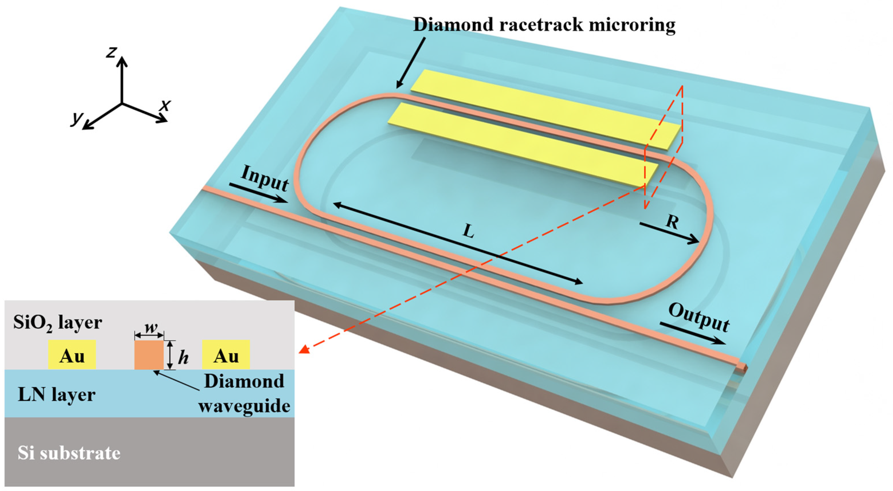
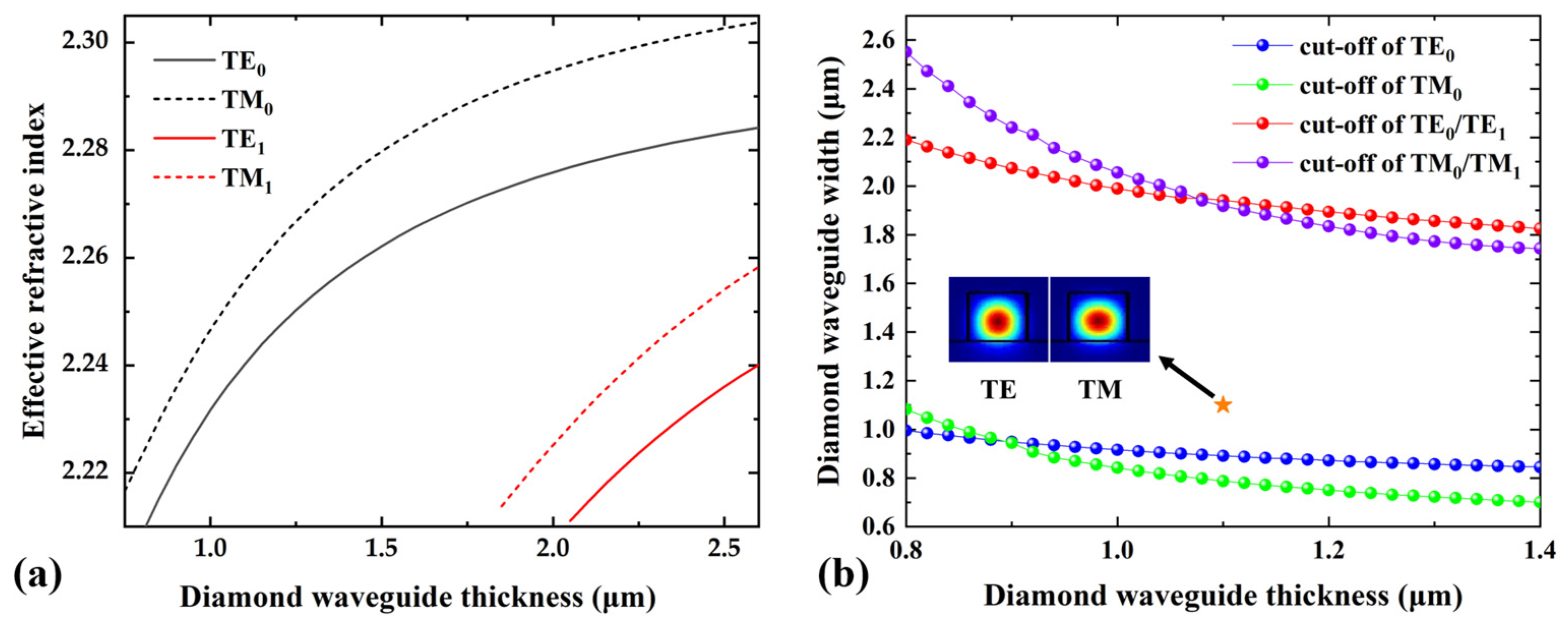
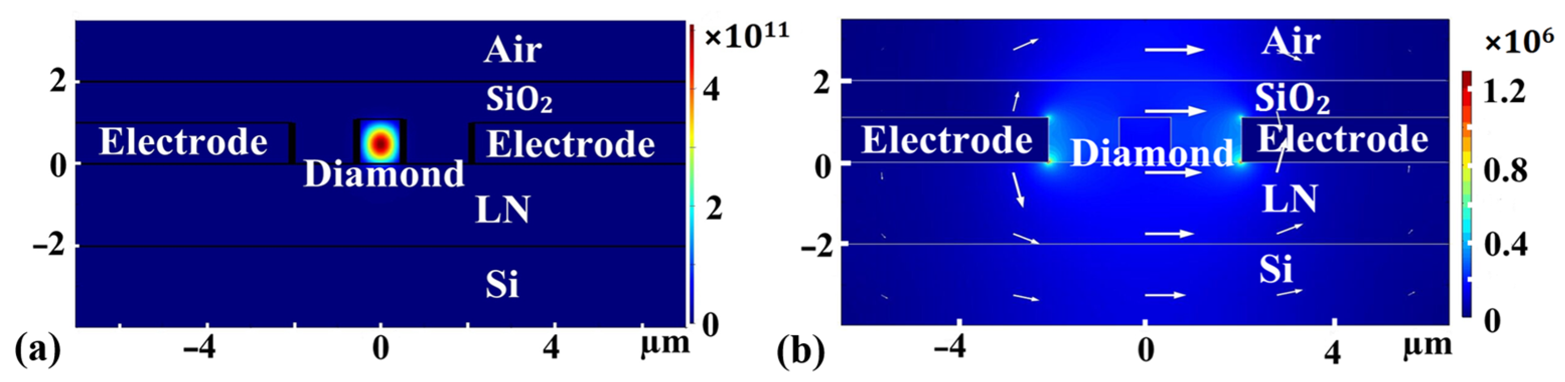
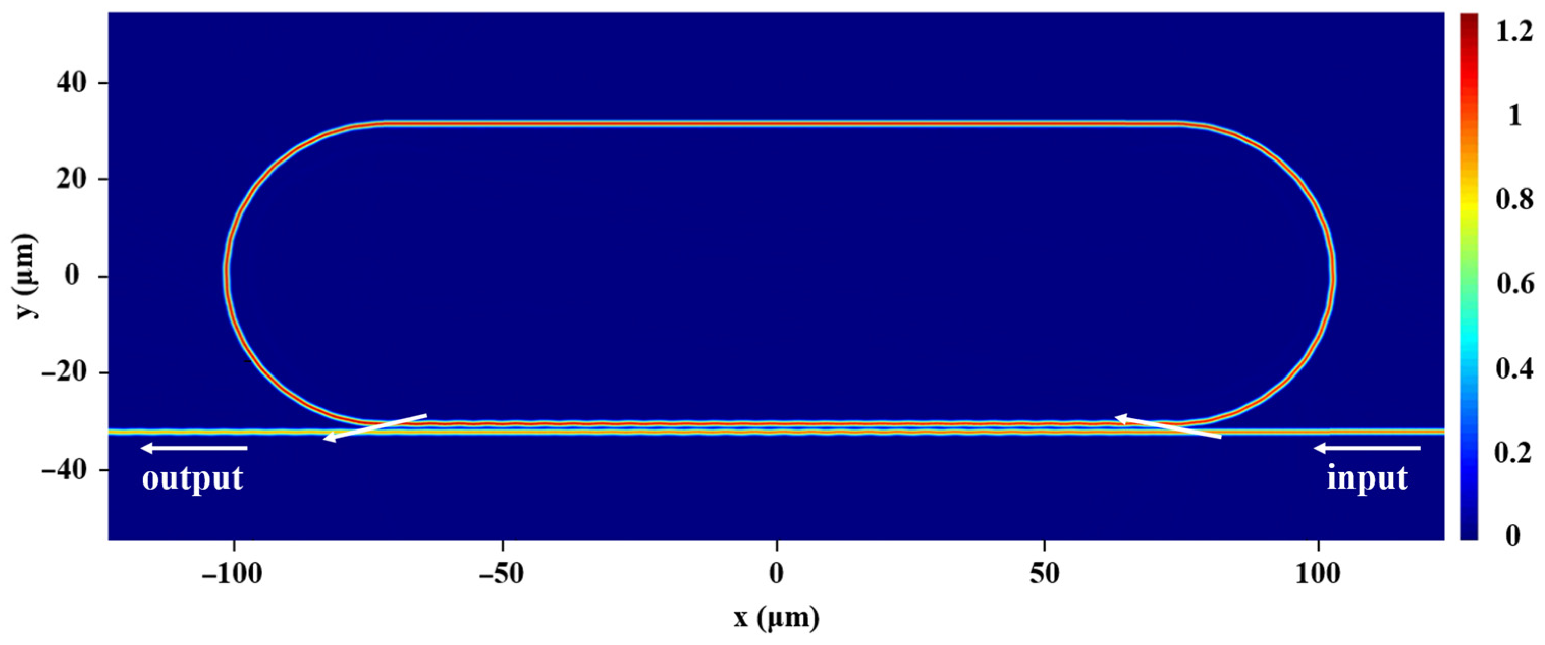
2. Design and Methods

The racetrack microring resonator on the diamond–LNOI hybrid platform comprises a diamond waveguide, an x-cut LNOI, a silicon substrate, and a SiO2 coating for packaging. The diamond racetrack microring resonator is embedded within the SiO2 coating layer, and gold (Au) electrodes are integrated on both sides of the microring track (Figure 1). In the inset of Figure 1, the red box highlights the cross-sectional view; R represents the bending radius of the microring; L denotes the length of the racetrack structure; and the x, y, and z axes signify the 3D-FDTD simulation directions. The choice of the x-cut orientation was based on its flexible electrode design, effectively harnessing the maximum E-O coefficient γ33 of x-cut LN. The racetrack microring resonator comprises a single straight waveguide and a racetrack microring. When the resonant conditions are met, light couples from the straight waveguide to the racetrack microring due to the presence of evanescent waves. Resonance reinforcement occurs as light re-enters the straight waveguide after circulating the microring, causing an optical path difference of integer multiples of the λ between the light in the racetrack microring and the straight waveguide, yielding optical amplification.
The refractive index, power ratio in LN, propagation loss, and bending loss are computed using the FDE technique. The quality factor (Q-factor) and free spectral range (FSR) are determined using the commercial software Lumerical FDTD Solutions 2020 R2 version (ANSYS Inc., South Pittsburg, PA, USA). PML boundary conditions were utilized to absorb emitted light within the simulation area [35].
The FDE technique is a numerical method used in the field of electromagnetics and optics to calculate the eigenmodes (or eigenfrequencies) of electromagnetic waveguides, resonators, and other structures. Eigenmodes represent the specific electromagnetic field patterns and frequencies that a given structure can support. This technique is particularly useful for analyzing and designing photonic and optoelectronic devices, such as optical waveguides, microcavities, and photonic crystals. In this method, the electromagnetic field equations, typically Maxwell’s equations, are discretized on a grid using finite-difference approximations. The grid divides the structure into small cells, and the equations are solved numerically for each cell while taking into account the boundary conditions. The goal is to find the solutions that satisfy the eigenvalue problem, where specific frequencies (eigenfrequencies) and corresponding field patterns (eigenmodes) are sought. These eigenmodes represent the fundamental modes or resonant modes supported by the structure. The FDE technique, as a tool for understanding the behavior of electromagnetic fields in complex structures, accurately predicts the resonant frequencies and mode distributions of various photonic and optoelectronic devices to optimize their performance.
In FDTD solutions, the vector three-dimensional Maxwell equations are discretized over both time and space using time-domain signals. This meticulous gridding process facilitates the acquisition of steady-state continuous wave solutions, resulting in a wide bandwidth for electromagnetic simulations. Additionally, a unique material model is integrated into the framework to accurately depict the dispersion characteristics of materials across a broad spectrum, and this model is bolstered by high-speed computing capabilities. With the assistance of high-performance computing engines, the method efficiently computes multiwavelength results in a single simulation run, rendering it a versatile and indispensable tool for researchers and engineers. This approach empowers simulations of diverse three-dimensional shapes while maintaining precision in modeling material dispersion. The 3D FDTD method is a robust numerical technique extensively employed in electromagnetic simulations. It entails the grid-based discretization of three-dimensional space and the iterative solution of Maxwell’s equations in the time domain. This methodology is particularly adept at yielding steady-state continuous wave solutions, rendering it exceptionally suitable for investigating a wide spectrum of electromagnetic phenomena.
Nonetheless, the FDTD method comes with inherent limitations, primarily linked to computational resources. The finite memory capacity and processing speed of computers typically confine FDTD simulations to specific spatial domains or volumes. To overcome this limitation when simulating ultrasonic wave propagation across larger areas, it becomes imperative to address wave reflections at simulation boundaries. This is where PML plays a crucial role. PML serves as an absorption boundary condition technique specifically designed to minimize wave reflections at the boundaries of a simulation domain. Unlike simpler boundary conditions, PML is engineered to theoretically achieve complete absorption of incoming waves, rendering it a valuable asset for accurately simulating wave propagation in extensive and complex environments. The implementation of PML empowers researchers to expand the computational domain of their FDTD simulations, ensuring the faithful representation of electromagnetic wave behavior in larger regions.
In essence, the 3D FDTD method is a potent numerical tool for simulating electromagnetic phenomena, with a strong focus on accurate dispersion modeling and wide bandwidth capabilities. To surmount limitations associated with computational resources and facilitate electromagnetic wave simulations over larger areas, the incorporation of PML absorption boundaries is essential, effectively minimizing wave reflections and enabling comprehensive simulations in intricate scenarios.

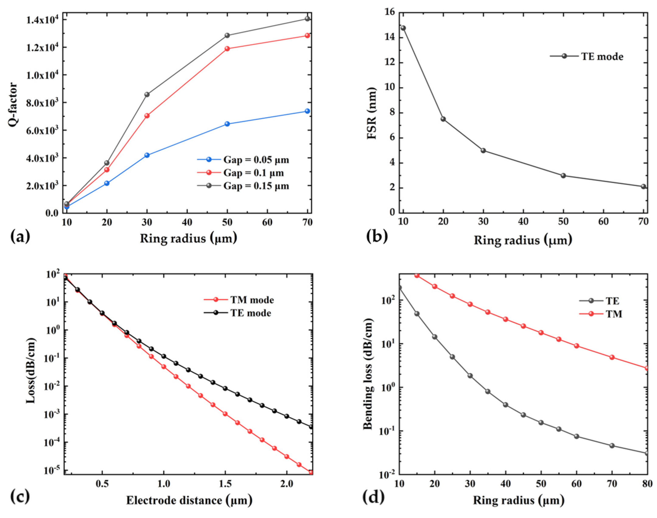
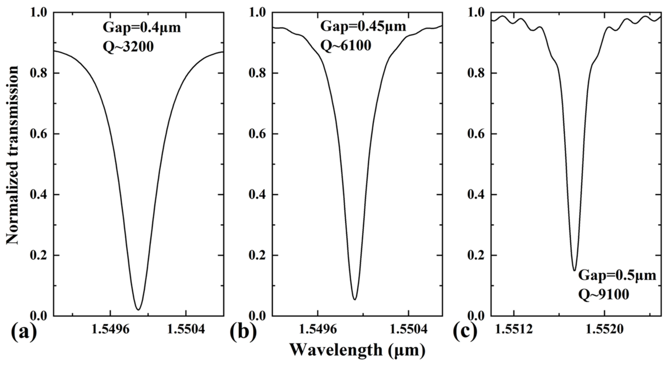
3. Results and Discussion

Achieving single-mode operation is crucial for microring resonators, as each mode in a multi-mode waveguide possesses a unique resonant wavelength. When closely spaced resonant wavelengths of various modes coexist, the transmission spectrum becomes disordered, causing signal distortion. To circumvent this issue and optimize performance, we determined the appropriate waveguide size for single-mode operation, alleviating signal distortion. Thus, the investigation into single-mode conditions not only enhanced efficiency but also ensured the reliability of optical waveguide systems.
Figure 2a illustrates the correlation between the effective refractive index (neff) and h of the diamond waveguide at a fixed w of 1.1 μm, corresponding to a wavelength of 1.55 μm, for the transverse electric (TE) mode and transverse magnetic (TM) modes. In the single-mode cutoff size range, only the fundamental TE (TE0) and fundamental TM (TM0) modes exist. An increasing waveguide thickness causes neff to rise, resulting in the emergence of multiple modes. The first-order TE (TE1) and first-order TM (TM1) modes appear when h exceeds 2.05 μm and 1.85 μm, respectively. Figure 2b depicts a cross-sectional view of the TE and TM modes when the diamond waveguide has a width and thickness of 1.1 μm, with the cut-off dimensions of the TE0 and TM0 modes and the TE1 and TM1 modes. For instance, with a 1.1 μm diamond waveguide thickness, the single-mode waveguide width ranges for the TE and TM modes are 0.891–1.942 μm and 0.788–1.918 μm, respectively. To ensure single-mode operation, the diamond waveguide’s thickness and width are set to 1.1 μm, as indicated by the star marker in Figure 2b, consistent across all diamond waveguides, including straight and bending waveguides and racetrack sections. The fundamental TE and TM modes are shown in the inset of Figure 2b.
Group velocity dispersion of waveguide modes near the pumping wavelength exhibits anomalous behavior due to third-order nonlinear phenomena, such as self-phase modulation, four-wave mixing, and cross-phase modulation [26]. Figure 3 illustrates the dispersion curves of diamond waveguides for the TE and TM modes, featuring a 1.1 μm thickness and a 1.1 μm width. At λ = 1.55 μm, the TE and TM modes demonstrate positive and negative dispersions, respectively, signifying normal and anomalous dispersions.
Key performance metrics of the microring resonator encompass coupling efficiency, Q-factor, and FSR. Q-factor and FSR are influenced by the radius and gap size, while the coupling efficiency is affected by the gap size and coupling length. The Q-factor is determined as follows [36]:
Q = π n g L λ 1     r 1 r 2 a 1     1     r 1 r 2 a ,
where L denotes the resonator length; r1 and r2 represent the loss coefficients, where r1 = r2; and a = exp(−αL⁄2), where α signifies the total loss in the ring, encompassing material absorption, radiation loss, and scattering loss due to wall roughness. Figure 4a showcases the correlation between the Q-factor and bending radius of the TE mode microring resonator (excluding the racetrack structure) for various gap sizes. For microring radii below 50 μm, the Q-factor exhibits a rapid increase as the radius grows. However, this increase in the Q-factor becomes less pronounced as the radius exceeds 50 μm. This behavior can be attributed to the reduction in radiation losses with larger curvature radii. Concurrently, as the microring length increases, the total propagation losses stabilize, leading to a more gradual increase in the Q-factor. The FSR, defined as the distance between neighboring resonant wavelengths, can be expressed as follows [36]:
F S R = λ 2 n g · L ,
where ng denotes the group refractive index:
n g = n e f f   λ d n e f f d λ .
In Figure 4b, the FSR of the racetrack microring resonators is computed for various radii through simulation using Lumerical FDTD Solutions 2020 R2 version software, considering h = w = 1.1 μm and wavelengths near 1.55 μm. The FSR decreases as the resonator length increases, resulting from the longer resonator lengths associated with larger radii. The racetrack microring yields a maximum FSR of 14.77 nm at a radius of 10 μm. However, as the radius increases further, for instance to 70 μm, the FSR decreases to 2.12 nm, which could be attributed to the corresponding increase in length due to larger radii. Figure 4c presents the relationship between bending loss and bending radius for the TE and TM modes in a diamond waveguide. Bending loss, computed using the FDE approach, diminishes with increasing radius, with the TE mode exhibiting significantly lower loss than the TM mode. The interaction between the evanescent wave and metal in the diamond waveguide increases the transmission loss, known as surface plasmon resonance. To examine the impact of the separation distance (D) between the electrode and diamond waveguide on propagation loss, we conducted a systematic study. The results in Figure 4d indicate that when the separation distance is relatively small, the waveguide’s mode field interacts with the metal, exciting surface plasmons and significantly increasing transmission loss. However, with increasing separation distance, the propagation loss gradually diminishes. For a separation distance exceeding 1.5 μm, the TE and TM modes exhibit propagation losses of less than 10−2 dB/cm. Consequently, the separation distance is set to 1.5 μm.
To fully leverage the E-O coefficient γ33 of x-cut LN, we focused exclusively on TE mode computations in subsequent simulations. We conducted structural optimization to strike a balance between the gap size and process complexity because an excessively small gap size challenges the processing. The racetrack structure was integrated into the microring, enhancing the coupling length and increasing the gap size. This modification ensured high coupling efficiency and mitigated processing difficulty. Figure 5 displays the transmission spectra of the racetrack microring resonator with various gap sizes, considering a racetrack length (Lr) and radius (R) of 150 μm and 30 μm, respectively. The results demonstrate that an increasing gap size enhances the Q-factor and diminishes the coupling efficiency. For a 0.4 μm gap, the coupling efficiency approaches 100%, but the corresponding Q-factor of 3200 is relatively low. In contrast, a gap size of 0.5 μm yields a higher Q-factor of 9100, but approximately 15% of light remains uncoupled into the ring. Therefore, a gap size of 0.45 μm achieves an optimal balance, with a high Q-factor (~6100) and a satisfactory coupling efficiency (~95%) for the racetrack microring resonator.
The resonant characteristics of the racetrack microring resonator rely on its length and refractive index. The resonant wavelength (λ) of the racetrack resonator can be defined as follows:
λ = n e f f   · L m ,
where neff represents the effective refractive index of the waveguide; and m is an arbitrary integer. Subsequently, we could deduce the following:
λ m = n 1 L 1 + L r + n 2 L r ,
where n1 and n2 signify the effective refractive indices of the waveguide without and with electric field intensity, respectively, and L1 denotes the length of the bend waveguide.
E-O tunability is pivotal in the performance of tunable racetrack microring resonators. Equation (5) highlights that the wavelength shift necessitates a change in the effective refractive index. However, diamond lacks E-O effects; therefore, increasing the electric field intensity has no impact on the refractive index of diamond. In contrast, lithium niobate exhibits E-O effects, and increasing the electric field intensity alters its refractive index, influencing the waveguide’s effective refractive index and causing wavelength shifts.
Figure 6a shows the distribution of light field intensity when the light (λ = 1.55 μm) propagates in the diamond waveguide. Most of the light is distributed in the diamond waveguide, and a small amount of light is distributed in the LN layer, so the refractive index of both diamond and LN has an effect on the effective refractive index of the waveguide. The effective refractive index of the waveguide could be changed by the change in the refractive index of LN when the electric field intensity is different. Figure 6b shows the distribution of the direct current electric field intensity when 1 V voltage is applied. In the figure, 1 V voltage is applied to the left Au electrode, and the right Au electrode is grounded. It can be seen that the electric field intensity generated between the electrodes completely includes the LN layer, and the electric field direction is parallel to the surface of LN and perpendicular to the propagation direction of light, which will change the ne of x-cut LN.
To observe and utilize this tunability, an electric field, assumed to be uniform, is generated between the electrodes on both sides of the waveguide by applying a voltage. Therefore, the extraordinary refractive indices of LN under various electric field intensities can be computed. By varying the intensity of the electric field voltage, we can determine Δne as follows:
Δ n e = 1 2 n e 2 γ 33 E z
where Ez represents the electric field intensity in the z-direction; and ne denotes the extraordinary refractive index. When the electric field intensity Ez is 1 V/μm, the change in extraordinary refractive index of LN (Δne) for a wavelength λ = 1.55 μm is 1.3 × 10⁻⁴. Subsequently, the strength of the photoelectric E-O effect can be modified by adjusting the applied electric field intensity and varying the resonant wavelength by controlling Δne.
An increasing electric field intensity causes larger extraordinary refractive index changes in LN, increasing the effective refractive index of the diamond waveguide and causing a resonance wavelength shift. To simulate variations in electric field intensity, different refractive indices are set for LN, and the FDE approach is employed to determine the effective refractive index of the TE mode at λ = 1.55 μm propagating in the diamond waveguide under various electric field intensities. Equation (5) is utilized to compute the resonant wavelength shift (ΔλTE) of the TE mode.
Table 1 shows the refractive index and dielectric constant of the materials used in the simulation, where the ne of LN can be substituted into Equation (6) to obtain the relationship between Δne and the electric field intensity, so as to obtain the ne under different electric field intensities. The effective refractive index of the waveguide with different electric field intensities can be obtained by using a different ne in the simulation. Then, the resonance wavelength offset under different electric field intensities can be obtained by using Equation (5).
Figure 7a depicts the optical power percentage of the TE mode in the LN layer for various diamond waveguide thicknesses at λ = 1.55 μm, computed using the FDE method. The results indicate that the percentage of optical power in the LN layer exhibits a negative correlation with the diamond waveguide thickness due to a higher optical power distribution within the diamond waveguide with increasing diamond waveguide thickness, resulting in a decreased proportion of optical power in lithium niobate. The diamond waveguide thicknesses of 1 μm, 1.1 μm, and 1.2 μm yield the optical power percentages of 8.69%, 6.84%, and 5.48%, respectively. The decrease in the percentage of optical power in LN weakens the electro-optical effect, resulting in a decrease in wavelength offset at the same electric field intensity, as shown in Figure 7b. The resonant wavelength shift for diamond waveguide thicknesses of 1 μm, 1.1 μm, and 1.2 μm at an electric field intensity of 15 V/μm are 33.62 pm, 27.64 pm, and 23.16 pm, respectively. When the thickness of the diamond waveguide is 1 μm, the fundamental mode of the TE mode is close to the cutoff size, so a thickness of 1.1 μm is suitable. The wavelength shift increases with rising electric field intensity, with wavelength shifts of 9.5 pm, 16.8 pm, and 27.6 pm at electric field intensities of 5 V/μm, 10 V/μm, and 15 V/μm, respectively. These findings exhibit a linear relationship between the wavelength shift and the electric field intensity. The tuning coefficient, representing the rate of change in the wavelength shift with respect to the electric field intensity, is 1.84 pm/V.
Figure 8 shows the electric field intensity distribution of light in a racetrack microring resonator. The incident light enters from the input end of the diamond/LNOI waveguide. When the light propagates in the waveguide and generates total reflection, there are evanescent waves, but when the gap between the straight waveguide and the racetrack is small enough, the evanescent waves could be coupled into the racetrack. When the light in the racetrack and the light in the straight waveguide meet the conditions of interference reinforcement, the coupling efficiency could be greatly improved. When the light in the racetrack passes through the output end around the microring, the wavelength that satisfies interference reinforcement is coupled into the straight waveguide and output from the output end, and the wavelength that does not satisfy the interference reinforcement condition cannot enter the straight waveguide.
Table 2 presents a list of different types of microring resonators reported previously, including diamond, Si3N4, Si, Ta2O5, chalcogenide, and direct etching, and compares them to this work. In this study, the combination of diamond waveguides with LNOI resulted in a larger FSR and extinction ratio, as well as an E-O tunability of 1.84 pm/V, with a Q-factor of approximately 6100. These outstanding performance characteristics in integrated optics applications contribute to the realization of high-performance, compact, and multifunctional optical components. These advantages and benefits render them a popular choice in micro/nano optical chips with photonic integration.

4. Conclusions

In this study, we have developed an E-O tunable racetrack microring resonator and assessed it on a diamond–LNOI hybrid integration platform using the 3D-FDTD and FDE approaches. Furthermore, we have determined the optimal device parameters: R, h, w, gap sizes, and D to be 30 μm, 1.1 μm, 1.1 μm, 0.45 μm, and 1.5 μm, respectively. The designed E-O tunable resonator showcases a high coupling efficiency and Q-factor of approximately 95% and 6100, respectively, at λ = 1.55 μm, and an FSR of 4.99 nm at Lr = 150 μm with a racetrack structure. A wavelength shift of 27.6 pm is achieved at an electric field strength of 15 V/μm, yielding a tuning factor of 1.84 pm/V. To mitigate the manufacturing complexity associated with smaller gap sizes while preserving coupling efficiency, a racetrack structure is incorporated to increase the gap size. This study offers valuable insights and practical guidelines for future research and fabrication of E-O tunable racetrack microring resonators, facilitating the integration of quantum and classical optical information on a single chip.

Author Contributions

Conceptualization, F.Y. and C.C.; methodology, F.Y. and Y.W.; software, F.Y. and Y.W.; validation, F.Y., Y.W., H.F. and C.C.; formal analysis, C.C.; investigation, F.Y., Y.W. and H.F.; resources, C.C.; data curation, C.C.; writing—original draft, F.Y. and Y.W.; writing—review and editing, F.Y., Y.W. and H.F.; visualization, F.Y.; supervision, C.C.; project administration, C.C.; funding acquisition, C.C. All authors have read and agreed to the published version of the manuscript.

Funding

This research was funded by the National Natural Science Foundation of China, grant numbers 12105190 and 61935014.

Data Availability Statement

The data used to support the findings of this study are included within the article.

Conflicts of Interest

The authors declare no conflict of interest.

References

  1. Hausmann, B.J.M.; Bulu, I.; Venkataraman, V.; Deotare, P.; Lončar, M. Diamond nonlinear photonics. Nat. Photonics 2014, 8, 369–374. [Google Scholar] [CrossRef]
  2. Faraon, A.; Barclay, P.E.; Santori, C.; Fu, K.C.; Beausoleil, R.G. Resonant enhancement of the zero-phonon emission from a colour centre in a diamond cavity. Nat. Photonics 2011, 5, 301–305. [Google Scholar] [CrossRef]
  3. Sanong, E.; Pimthong, T. Transflectance Spectra of Faceted Diamonds Acquired by Infrared Microscopy. Appl. Spectrosc. 2005, 59, 1160–1165. [Google Scholar] [CrossRef]
  4. Evans, R.E.; Bhaskar, M.K.; Sukachev, D.D.; Nguyen, C.T.; Sipahigil, A.; Burek, M.J.; Machielse, B.; Zhang, G.H.; Zibrov, A.S.; Bielejec, E.; et al. Photon-mediated interactions between quantum emitters in a diamond nanocavity. Science 2018, 362, 662–665. [Google Scholar] [CrossRef]
  5. Shandilya, P.K.; Flågan, S.; Carvalho, N.C.; Zohari, E.; Kavatamane, V.K.; Losby, J.E.; Barclay, P.E. Diamond Integrated Quantum Nanophotonics: Spins, Photons and Phonons. J. Light. Technol. 2022, 40, 7538–7571. [Google Scholar] [CrossRef]
  6. Ge, F.; Chen, B.; Wang, Y.; Zhou, F.; Zheng, R.; Yang, X.; Qian, P.; Xu, N. A Wideband Balun-Based Microwave Device for Quantum Information Processing with Nitrogen–Vacancy Centers in Diamond. J. Light. Technol. 2022, 40, 7572–7577. [Google Scholar] [CrossRef]
  7. Wickenbrock, A.; Zheng, H.; Bougas, L.; Leefer, N.; Afach, S.; Jarmola, A.; Acosta, V.M.; Budker, D. Microwave-free magnetometry with nitrogen-vacancy centers in diamond. Appl. Phys. Lett. 2016, 109, 053505. [Google Scholar] [CrossRef]
  8. Aharonovich, I.; Greentree, A.D.; Prawer, S. Diamond photonics. Nat. Photonics 2011, 5, 397–405. [Google Scholar] [CrossRef]
  9. Josset, S.; Muller, O.; Schmidlin, L.; Pichot, V.; Spitzer, D. Nonlinear optical properties of detonation nanodiamond in the near infrared: Effects of concentration and size distribution. Diam. Relat. Mater. 2013, 32, 66–71. [Google Scholar] [CrossRef]
  10. Levenson, M.D.; Bloembergen, N. Dispersion of the nonlinear optical susceptibility tensor in centrosymmetric media. Phys. Rev. B 1974, 10, 4447–4463. [Google Scholar] [CrossRef]
  11. Dong, X.; Wang, T.; Lu, Z.; An, Y.; Wang, Y. Computational design of reliable intermediate-band photovoltaic absorber based on diamond. Opt. Express 2023, 31, 18227–18239. [Google Scholar] [CrossRef] [PubMed]
  12. Ahmed, A.N.R.; Shi, S.; Zablocki, M.; Yao, P.; Prather, D.W. Tunable hybrid silicon nitride and thin-film lithium niobate electro-optic microresonator. Opt. Lett. 2019, 44, 618–621. [Google Scholar] [CrossRef] [PubMed]
  13. Snigirev, V.; Riedhauser, A.; Lihachev, G.; Churaev, M.; Riemensberger, J.; Wang, R.N.; Siddharth, A.; Huang, G.; Möhl, C.; Popoff, Y.; et al. Ultrafast tunable lasers using lithium niobate integrated photonics. Nature 2023, 615, 411–417. [Google Scholar] [CrossRef]
  14. Hausmann, B.J.M.; Choy, J.T.; Babinec, T.M.; Shields, B.J.; Bulu, I.; Lukin, M.D.; Lonvcar, M. Diamond nanophotonics and applications in quantum science and technology. Phys. Status Solidi A 2012, 209, 1619–1630. [Google Scholar] [CrossRef]
  15. Schröder, T.; Mouradian, S.L.; Zheng, J.; Trusheim, M.E.; Walsh, M.; Chen, E.H.; Li, L.; Bayn, I.; Englund, D. Quantum nanophotonics in diamond. J. Opt. Soc. Am. B 2016, 33, B65–B83. [Google Scholar] [CrossRef]
  16. Liu, Y.; Wang, Q.; Qin, Y.; Guo, H.; Li, J.; Li, Z.; Wen, H.; Ma, Z.; Tang, J.; Liu, J. Microwave target location method based on diamond NV color center. Appl. Optics 2023, 62, 4275–4280. [Google Scholar] [CrossRef]
  17. Omar, M.; Conta, A.; Westerhoff, A.; Hasse, R.; Chatzidrosos, G.; Budker, D.; Wickenbrock, A. Diamond-optic enhanced photon collection efficiency for sensing with nitrogen-vacancy centers. Opt. Lett. 2023, 48, 2512–2514. [Google Scholar] [CrossRef] [PubMed]
  18. Poberaj, G.; Hu, H.; Sohler, W.; Günter, P. Lithium niobate on insulator (LNOI) for micro-photonic devices. Laser Photonics Rev. 2012, 6, 488–503. [Google Scholar] [CrossRef]
  19. Han, H.; Cai, L.; Hu, H. Optical and structural properties of single-crystal lithium niobate thin film. Opt. Mater. 2015, 42, 47–51. [Google Scholar] [CrossRef]
  20. Palm, K.J.; Dong, M.; Golter, D.A.; Clark, G.; Zimmermann, M.; Chen, K.C.; Li, L.; Menssen, A.; Leenheer, A.J.; Dominguez, D.; et al. Modular chip-integrated photonic control of artificial atoms in diamond nanostructures. Optica 2023, 10, 634–641. [Google Scholar] [CrossRef]
  21. Han, H.; Xiang, B. Integrated electro-optic modulators in x-cut lithium niobate thin film. Optik 2020, 212, 164691. [Google Scholar] [CrossRef]
  22. Langrock, C.; Diamanti, E.; Roussev, R.V.; Yamamoto, Y.; Fejer, M.M.; Takesue, H. Highly efficient single-photon detection at communication wavelengths by use of upconversion in reverse-proton-exchanged periodically poled LiNbO3 waveguides. Opt. Lett. 2005, 30, 1725–1727. [Google Scholar] [CrossRef] [PubMed]
  23. Lu, H.; Xiong, H.; Huang, Z.; Li, Y.; Dong, H.; He, D.; Dong, J.; Guan, H.; Qiu, W.; Zhang, X.; et al. Electron-plasmon interaction on lithium niobate with gold nanolayer and its field distribution dependent modulation. Opt. Express 2019, 27, 19852–19863. [Google Scholar] [CrossRef] [PubMed]
  24. Liu, Y.; Li, H.; Liu, j.; Tan, S.; Lu, Q.; Guo, W. Low Vπ thin-film lithium niobate modulator fabricated with photoliography. Opt. Express 2021, 29, 6320–6329. [Google Scholar] [CrossRef]
  25. Ahmed, A.N.R.; Shi, S.; Mercante, A.J.; Prather, D.W. High-performance racetrack resonator in silicon nitride -thin film lithium niobate hybrid platform. Opt. Express 2019, 27, 30741–30751. [Google Scholar] [CrossRef]
  26. Wu, Y.; Zong, R.; Han, H.; Lu, S.; Lin, J.; Xie, H.; Zhang, Y.; Ruan, S.; Han, P.; Xiang, B. Design of an electro-optical tunable race-track diamond microring resonator on lithium niobate. Diam. Relat. Mater. 2021, 120, 108692. [Google Scholar] [CrossRef]
  27. Desiatov, B.; Shams-Ansari, A.; Zhang, M.; Wang, C.; Loncar, M. Ultra-low-loss integrated visible photonics using thin-film lithium niobate. Optica 2019, 6, 380–384. [Google Scholar] [CrossRef]
  28. Cheng, Q.; Dai, L.Y.; Abrams, N.C.; Hung, Y.; Morrissey, P.E.; Glick, M.; O’Brien, P.; Bergman, K. Ultralow-Crosstalk, Strictly Non-Blocking Microring-Based Optical Switch. Photonics Res. 2019, 7, 155–161. [Google Scholar] [CrossRef]
  29. Chen, G.; Jiang, C. Reverse design of microring resonator channel dropping filters. Results Phys. 2020, 19, 103380. [Google Scholar] [CrossRef]
  30. Bahadori, M.; Goddard, L.L.; Gong, S. Fundamental Electro-Optic Limitations of Thin-film Lithium Niobate Microring Modulators. Opt. Express 2020, 28, 13731–13749. [Google Scholar] [CrossRef]
  31. Han, H.; Xiang, B.; Lin, T.; Chai, G.; Ruan, S. Design and Optimization of Proton Exchanged Integrated Electro-Optic Modulators in X-Cut Lithium Niobate Thin Film. Crystals 2019, 9, 549. [Google Scholar] [CrossRef]
  32. Maiti, R.; Patil, C.; Saadi, M.A.S.R.; Xie, T.; Azadani, J.G.; Uluutku, B.; Amin, R.; Briggs, A.F.; Miscuglio, M.; Thourhout, D.V.; et al. Strain-Engineered High Responsivity MoTe2 Photodetector for Silicon Photonic Integrated Circuits. Nat. Photonics 2019, 14, 578–584. [Google Scholar] [CrossRef]
  33. Hu, Y.; Yu, M.; Buscaino, B.; Sinclair, N.; Zhu, D.; Cheng, R.; Shams-Ansari, A.; Shao, L.; Zhang, M.; Kahn, J.M.; et al. High-efficiency and broadband on-chip electro-optic frequency comb generators. Nat. Photonics 2022, 16, 679–685. [Google Scholar] [CrossRef]
  34. Lumerical Solutions. Available online: http://www.lumerical.com/ (accessed on 15 July 2023).
  35. Shibayama, J.; Ando, R.; Yamauchi, J.; Nakano, H. A 3-D LOD-FDTD Method for the Wideband Analysis of Optical Devices. J. Light. Technol. 2011, 29, 1652–1658. [Google Scholar] [CrossRef]
  36. Rabiei, P.; Steier, W.H.; Zhang, C.; Dalton, L.R. Polymer micro-ring filters and modulators. J. Light. Technol. 2002, 20, 1968–1975. [Google Scholar] [CrossRef]
  37. Wong, K.K. Properties of Lithium Niobate, 1st ed.; INSPEC: London, UK, 2002; pp. 115–128. [Google Scholar]
  38. Mahmoud, M.; Cai, L.; Bottenfield, C.; Piazza, G. Lithium Niobate Electro-optic Racetrack Modulator Etched in Y-Cut LNOI Platform. IEEE Photonics J. 2018, 10, 1–10. [Google Scholar] [CrossRef]
  39. Hausmann, B.; Bulu, I.; Deotare, P.; McCutcheon, M.; Venkataraman, V.; Markham, M.; Twitchen, D.; Loncar, M. Integrated High-Quality Factor Optical Resonators in Diamond. Nano Lett. 2013, 13, 1898–1902. [Google Scholar] [CrossRef]
  40. Wu, Z.; Lin, Y.; Han, S.; Yin, X.; Ding, M.; Guo, L.; Yang, X.; Zhao, M. Simulation and Analysis of Microring Electric Field Sensor Based on a Lithium Niobate-on-Insulator. Crystals 2021, 11, 359. [Google Scholar] [CrossRef]
  41. Chen, L.; Wood, M.; Reano, R. 12.5 pm/V hybrid silicon and lithium niobate optical microring resonator with integrated electrodes. Opt. Express 2013, 21, 27003–27010. [Google Scholar] [CrossRef]
  42. Han, H.; Xiang, B. Simulation and analysis of electro-optic tunable microring resonators in silicon thin film on lithium niobate. Sci. Rep. 2019, 9, 6302. [Google Scholar] [CrossRef]
  43. Rao, A.; Patil, A.; Chiles, J.; Malinowski, M.; Novak, S.; Richardson, K.; Rabiei, P.; Fathpour, S. Heterogeneous microring and Mach-Zehnder modulators based on lithium niobate and chalcogenide glasses on silicon. Opt. Express 2015, 23, 22746–22752. [Google Scholar] [CrossRef] [PubMed]
  44. Rabiei, P.; Ma, J.; Khan, S.; Chiles, J.; Fathpour, S. Heterogeneous lithium niobate photonics on silicon substrates. Opt. Express 2013, 21, 25573–25581. [Google Scholar] [CrossRef] [PubMed]
Figure 1. Structure of a diamond racetrack microring resonator. Inset: schematic of cross-section of diamond on LNOI.
Electronics 12 04616 g001
Figure 2. (a) Correlation between the effective refractive index (TE and TM modes) and the width at λ = 1.55 µm. (b) Variation in the cut-off dimension as a function of diamond waveguide thickness and width at λ = 1.55 µm. Inset: mode profile of the fundamental TE and TM modes.
Electronics 12 04616 g002
Figure 3. Dispersion curves of TE and TM modes at h = 1.1 μm and w = 1.1 μm.
Electronics 12 04616 g003
Figure 4. Correlations between (a) Q-factor and bending radii at various gaps in the TE mode (excluding racetrack structure) and (b) FSR and bending radii in the TE mode. (c) The bending loss of the TE and TM modes. (d) The propagation loss of the TE mode in the diamond waveguide with varying electrode distances.
Electronics 12 04616 g004
Figure 5. Normalized transmission spectra of the TE mode in racetrack microring resonator with gap sizes of (a) 0.4 μm, (b) 0.45 μm and (c) 0.5 μm.
Electronics 12 04616 g005
Figure 6. (a) Distribution of light field intensity in diamond waveguide at λ = 1.55 μm. (b) Distribution of electric field intensity when 1 V voltage is applied to the electrode.
Electronics 12 04616 g006
Figure 7. (a) Percentage of optical power distributed in the LN layer as a function of diamond waveguide thickness. (b) Resonant wavelength shift for diamond waveguide thicknesses of 1 μm, 1.1 μm, and 1.2 μm at an electric field intensity of 15 V/μm.
Electronics 12 04616 g007
Figure 8. Distribution of electric field intensity of light in racetrack microring resonator.
Electronics 12 04616 g008
Table 1. The refractive indices and dielectric constants at λ = 1.55 μm of the materials used in the simulation.
MaterialRefractive IndexDielectric Constant
Ordinary
Refractive Index (no)
Extraordinary
Refractive Index (ne)
LN [37]2.2112.13828.4
Si3.4812.1
Diamond2.3845.7
Table 2. Performance comparison of microring resonator.
Type of ResonatorQ-FactorFSR (nm)Operating
Wavelength (μm)
Extinction Ratio (dB)E-O Tunability Tunability
(pm/V)
Ref
Diamond microring resonator1 × 1067.51545.1 (TE)3-[1]
Si3N4 strip-loaded microring on x-cut LNOI1.8 × 1050.581551.98 (TE)26.921.78[12]
Si3N4 strip-loaded racetrack resonator on x-cut LNOI1.3 × 1050.2071550.1 (TE)422.9[25]
Etched microring on x-cut LNOI7.8 × 106~0.59637 (TE)~16-[27]
Fourth-order filter 101550>50-[29]
Racetrack modulator etched on y-cut LNOI4.8 × 104~0.651549.8 (TE)>100.32[38]
Diamond microring resonator2.5 × 105~31550 (TE)~4.56-[39]
Etched microring on z-cut LNOI1 × 106-1550 (TM)~4.348[40]
Si waveguide racetrack resonator on z-cut LNOI1.15 × 1047.151552 (TM)~8.512.5[41]
Si waveguide resonator on z-cut LNOI~1 × 10412.51550 (TM)>2014.6[42]
Ge23Sb7S70 waveguide on y-cut LNOI1.2 × 105~0.831550 (TE)133.2[43]
Ta2O5 waveguide on y-cut LNOI~7.2 × 10⁴~1.151550 (TE)20-[44]
Diamond waveguide racetrack resonator on x-cut LNOI~61004.991550 (TE)~131.84This work
Disclaimer/Publisher’s Note: The statements, opinions and data contained in all publications are solely those of the individual author(s) and contributor(s) and not of MDPI and/or the editor(s). MDPI and/or the editor(s) disclaim responsibility for any injury to people or property resulting from any ideas, methods, instructions or products referred to in the content.

