1. Introduction
Clustering is the task of grouping sets of objects so that objects in the same group are more similar to each other than objects in other groups. Each group is referred to as a cluster, and this task is called clustering. Clustering results can be used for statistical data analysis that is used in many applications. Researchers and engineers have employed a variety of cluster models and clustering algorithms. Hierarchical clustering [
1] was the earliest clustering method that is based on distance connectivity. The expectation-maximization algorithm [
2] is one of the probability model-based approaches using statistical distributions, such as multivariate normal distributions. The k-means algorithm [
3] is another popular alternative for clustering, in which each cluster is represented by a single mean vector. K-means clustering has been widely studied with various extensions and applied in a variety of substantive areas.
The self-organizing map (SOM) [
4] is a type of unsupervised artificial neural network. The main feature of SOM is the nonlinear mapping of high-dimensional vectors onto a low-dimensional map of neurons, which has similar characteristics to the conventional clustering methods. With this feature, SOMs have been successfully used in a wide range of applications. Brito et al. [
5] proposed a method for cluster visualization using the SOMs. Zhang et al. [
6] presented a visual tracking of objects in video sequences. Gorzalczany et al. [
7] applied SOM to complex cluster analysis problems. Campoy et al. [
8] proposed a time-enhanced SOM and applied it to low-rate image compression.
The size of a SOM, i.e., the number of neurons, depends on the type of application, and certain applications require a large SOM. For some applications, SOM must handle high-dimensional vectors. For SOMs to process an image, the image is converted into vectors, but even a small image becomes a high-dimensional vector. Simulating SOMs in software is efficient because its flexibility makes it possible to easily change the SOM configurations, such as the number of neurons and vector dimensions. However, the computational cost of the large SOM and high-dimensional vector computation are too high for software SOMs. In such cases, an application-specific hardware SOM accelerator is highly desirable, and various custom hardware SOMs have been proposed [
9].
In our previous work, nested architecture for the SOM was proposed [
10]. The architecture is based on a homogeneous modular structure to provide easy expandability. The nested hierarchical architecture consists of multiple modules, and each module is made up of sub-modules. All modules have a similar structure, which makes it easier for designers to design a large hardware SOM.
Field-programmable gate array (FPGA) is a suitable and commonly used platform for implementing hardware SOMs, and hardware description languages (HDLs) are widely used. It is recommended to divide the large HDL model into hierarchies so that the synthesis tools can run more efficiently, and the hierarchical design makes it easier to write smaller modules if the design is broken up into smaller modules [
11]. In our previous work, performance analysis of the nested SOM architecture under various place-and-route (PAR) implementation strategies was not carried out. The PAR result can be evaluated by the worst negative slack (WNS) against the target clock constraint, which estimates the operation speed.
The previous work [
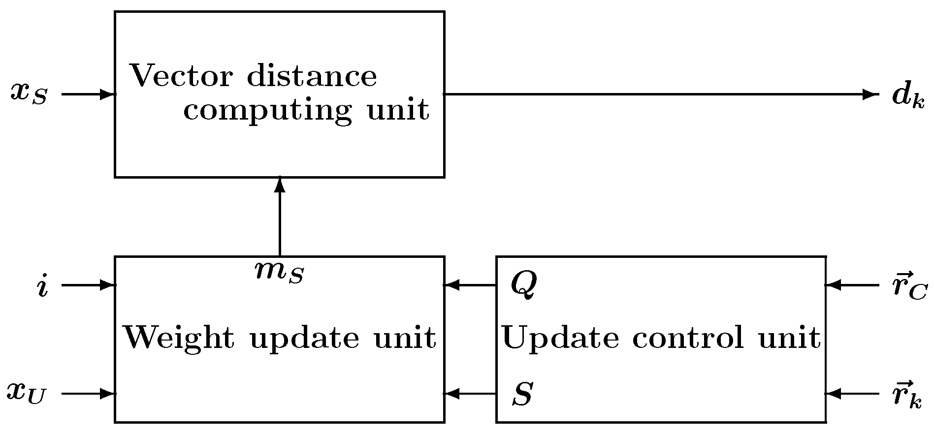
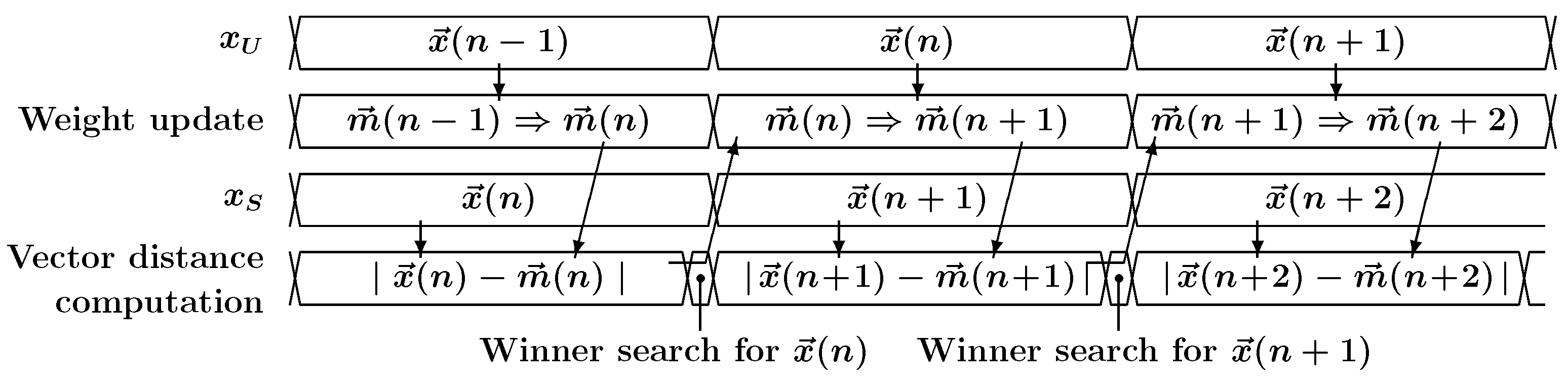
10] was designed to do the clustering of high-dimensional vectors by processing the vector elements sequentially. The sequential computation requires many clocks to process the one input vector, which significantly reduces overall throughput. The throughput can be improved by taking advantage of the parallelism embedded in the SOM computation. Therefore, parallel computing architectures are suitable for implementing SOM. Parallel computing systems can be constructed using temporal parallelism, spatial parallelism, or both. The pipelining of calculations is one of the common approaches to speed up calculations. It exploits temporal parallelism, where the processing task is partitioned into multiple steps, and the task is parallelized by executing the partitioned steps by different computing elements sequentially. To cope with the problem, the previous SOM incorporated simple pipeline computing. The learning process of the SOM consists of a winner search and a weight vector update. This pipeline operation of the architecture made it possible to compute the winner search and the weight update concurrently.
As stated above, designing a nested SOM architecture must consider WNS or the critical path more carefully, which motivates the paper to analyze various WNS-oriented implementation strategies and to add a pipeline stage. The contributions of this paper are summarized as follows:
- (1)
Analysis of the nested architecture’s impact on the PAR
Hardware SOMs with nested and flat architectures are described by VHDL, and their implementations are carried out by FPGA development tools. Then, their results are compared to reveal the efficiency of the nested architecture. In addition, the operating speeds of the two SOMs are compared through FPGA experiments to confirm the nested architecture efficiency.
- (2)
Enhancement of the pipeline computation
The higher the clock frequency, the higher the SOM’s performance becomes. To allow operation at the higher clock frequency, pipeline stages are increased in the winner search and the weight update.
The remainder of this paper is organized as follows.
Section 2 describes the SOM algorithm, and related hardware SOMs in the literature are briefly surveyed in
Section 3. The details of the nested SOM architecture are discussed in
Section 4. The results of the FPGA implementations and experiments are presented in
Section 5, and the results are discussed in
Section 6. Finally, the paper is concluded in
Section 7.
2. Self-Organizing Map Algorithms
The SOM consists of neurons typically placed in a two-dimensional grid, and all neurons include weight vectors. Neuron-
k includes a
D-dimensional weight vector
, which is made up of vector elements
’s.
The operation of the SOM can be divided into two phases: learning and recall. In the learning phase, a map is trained with a set of training vectors. Afterward, the weight vectors of neurons are retained, and the map is used in the recall phase.
The learning phase starts with an appropriate initialization of the weight vectors. Subsequently, the input vectors,
, are presented to the map in multiple iterations.
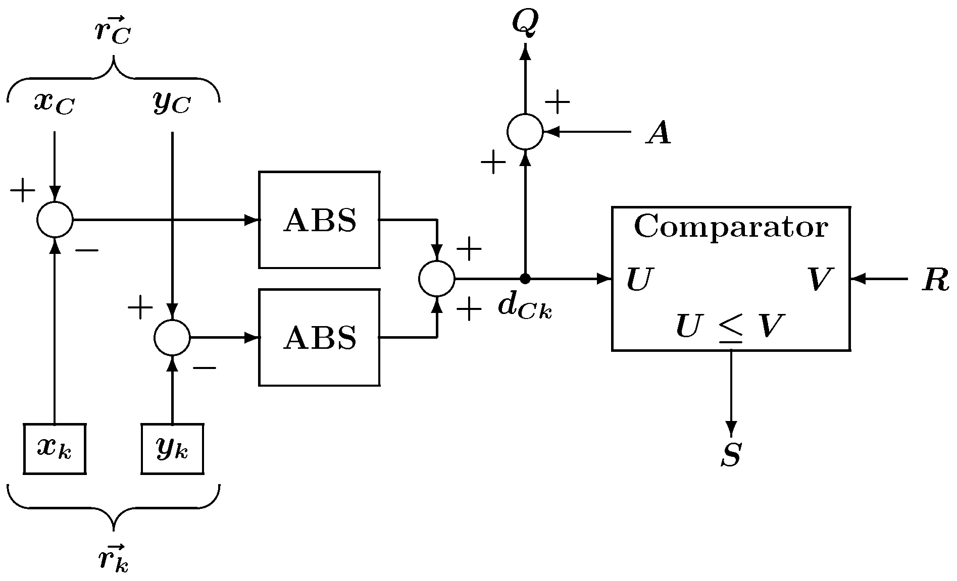
For each input vector, the distances to all weight vectors are calculated, and neuron-
C with the shortest distance is searched. This neuron-
C is called the winner neuron.
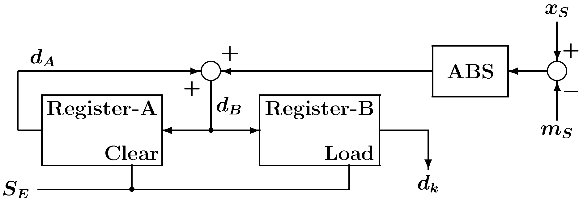
Euclidean distance was originally used for the vector distance
, but its hardware cost is too high. Thus, many hardware SOMs utilize the following Manhattan distance [
9].
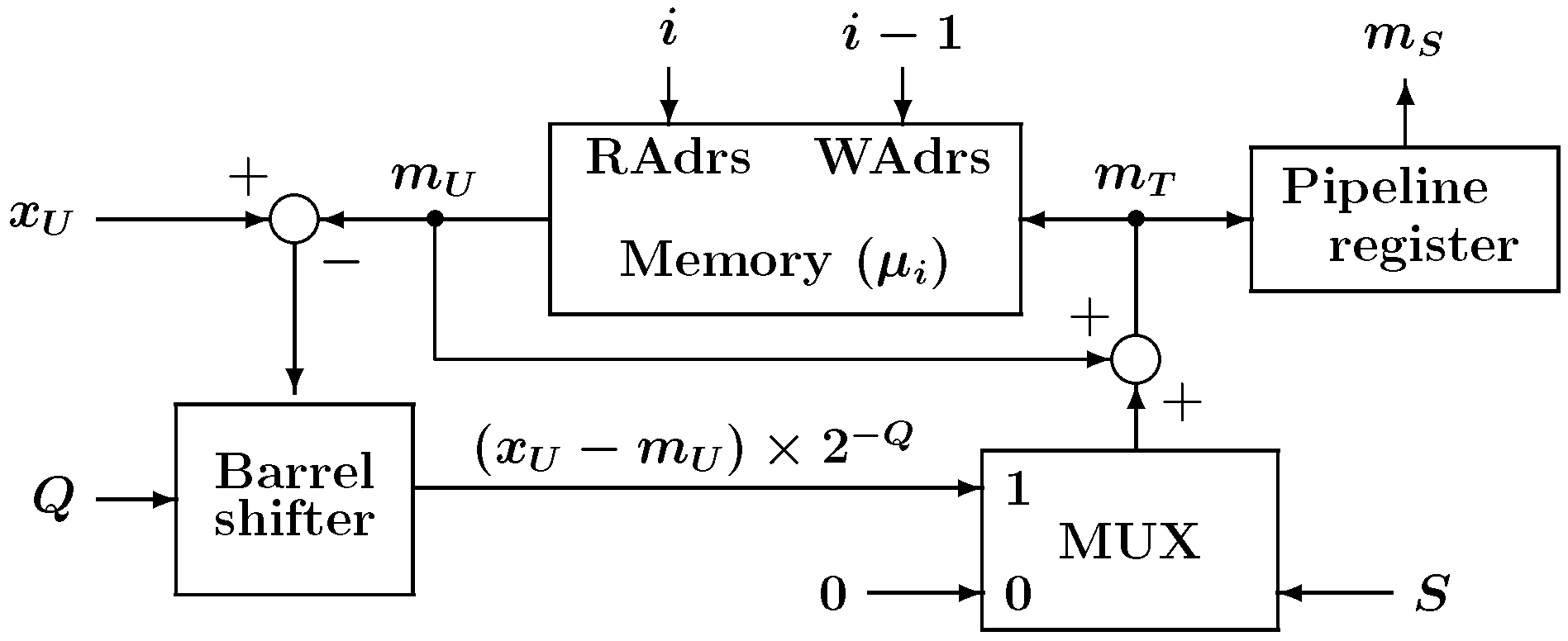
After the winning neuron is determined, the weight vectors of neurons in the vicinity of the winner neuron-
C are adjusted toward the input vector.
Here,
is called the neighborhood function and is defined as follows:
where
is the learning rate and
defines the size of the neighborhood, both of which decrease as the learning progresses (
t is the number of learning iterations).
and
are position vectors of the winner neuron-
C and neuron-
k, respectively. With this neighborhood function, vectors that are close to each other in the input space are also represented closer to each other on the map. This topology-preserving nature is a very important feature of the SOM. Like the Euclidean distance computation, the neighborhood function in Equation (
6) is too complicated for hardware implementation, so many hardware SOM utilize simplified neighborhood functions such as negative powers of two or a step function [
9].
3. Related Work
The researchers implemented the SOM algorithm on parallel computing hardware consisting of many processing elements (PEs). Such parallel architectures include those that consist of PEs that operate in a single-instruction-multiple-data (SIMD) manner. Porrmann et al. [
12] implemented a SOM on the universal rapid prototyping system RAPTOR2000, which consists of SIMD PEs. Multiple neurons could be implemented in each PE. The RAPTOR2000 system consisted of Xilinx Virtex FPGAs. Then, Porrmann et al. [
13] proposed another hardware accelerator. They developed the NBX neuro processor with CMOS technology, which was made up of eight PEs and worked in SIMD mode, and the Multiprocessor System for Neural Applications (MoNA) was developed by integrating the NBX neuro processors. The original SOM algorithm was modified to facilitate implementation in parallel hardware. Specifically, the Manhattan distance was used. Lachmair et al. [
14] proposed gNBXe, a hardware SOM based on a modular architecture. This work was based on the principles of NBX [
12]. It consisted of a global controller (GC) and the PEs that executed the neurons. The system could be easily extended by adding the gNBXe modules to the system bus. The instruction set of the PE was modified to implement Conscience SOM (CSOM).
Array processor is another parallel processing system in which the PEs are placed in an array structure. The array processor is suitable for the implementation of the SOM algorithm, too. Ramirez-Agundis et al. [
15] proposed a modular, massively parallel hardware SOM. The hardware architecture was divided into a processing unit array, an address generator, and a control unit. The processing unit array was distributed into modules, with 16 units each and a maximum of 16 modules (up to 256 neurons). The proposed system was applied to a vector quantizer for real-time video coding. Tamukoh et. al. [
16] proposed a winner search circuit, which was a modified version of bit-serial comparison. The proposed winner search performed a rough comparison in the early stage and a strict comparison in the later stage, which provided faster learning for massively parallel SOM architectures.
Kung [
17] proposed the systolic array, which is a homogeneous network of PEs. The PEs communicate only with their neighboring PEs to receive and deliver the computing data. As its name suggests, the propagation of data through a systolic array resembles the pulse of the human circulatory system. Like other parallel computing systems, the systolic array can be used to implement the hardware SOM. Manolakos et al. [
18] designed a modular SOM systolic architecture. The proposed array was made up of two types of PEs: the recall mode PE (PER) and the weights update PE (PEU). The proposed SOM was implemented on an FPGA, and a real-time vector classification problem was performed. They also developed a soft IP core in synthesizable VHDL, where the network size, vector dimension, etc. were configured by parameters. Jovanovic et al. [
19] implemented a hardware SOM that used network-on-chip (NoC) communication. NoC is a network-based communication subsystem on an integrated circuit. Its key feature is that the architecture can perform different applications in a time-sharing manner by dynamically defining the use of neurons and their interconnections. The proposed hardware SOM architecture also utilized the systolic way of data exchange through the NoC, which provided high flexibility and scalability. Ben Khalifa et al. [
20] proposed a modular SOM architecture called systolic-SOM (SSOM). The proposed architecture is based on the use of a generic model inspired by systolic movement and was formed by two levels of nested parallelism of neurons and connections. The systolic architecture was based on a concept in which a single data path traversed all neural PEs and was extensively pipelined.
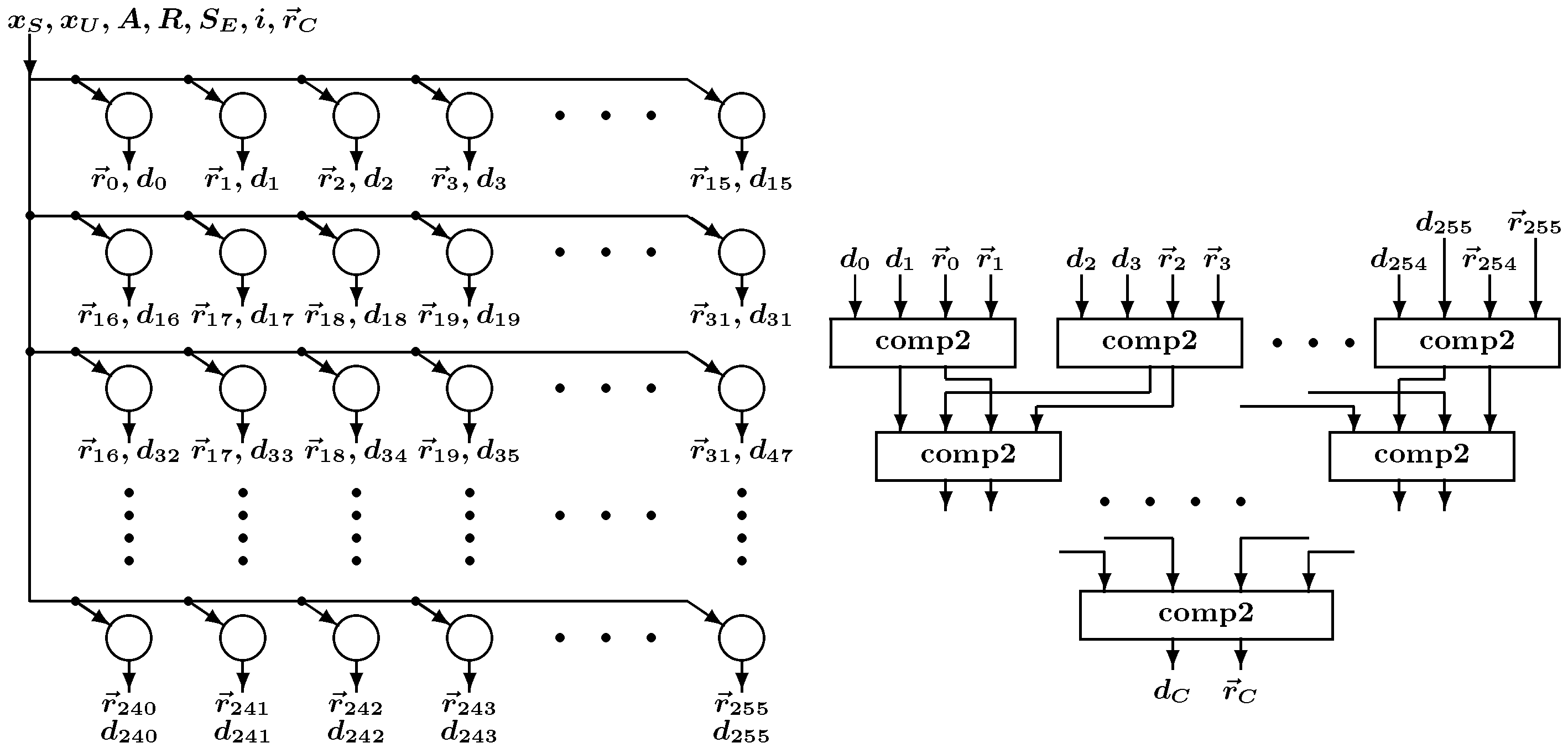
In the hardware SOM, the winner search is the key process that governs overall SOM’s computing speed because it must compare all vector distances of the neurons to find the smallest one. Researchers focused on effective methods to implement the winner search. de Abreu de Sousa et al. [
21] compared three different FPGA hardware architectures—centralized, distributed, and hybrid—for executing SOM learning and recall phases. The centralized architecture used a central control unit that found the global winner and controlled all computation units. In the distributed architecture, local winners of neuron groups were identified, and the global winner was selected from them. The hybrid model combined the two architectures. Three architectures were compared in terms of chip area occupation and maximum operating frequency, and the results revealed that the centralized model outperformed the other models. All Winner-SOM (AW-SOM) proposed by Cardarilli et al. [
22] did not require the identification of the winner neuron, which is a crucial operation in terms of propagation delay. Experimental results showed that if the neurons were initialized using a uniform or random distribution, the results of AW-SOM and traditional SOM clustering were comparable in 92% of the cases. The absence of the comparator tree for the winner neuron selection considerably improved the system performance.
Various applications were applied to the hardware SOMs in the literature, such as image enlargement [
16], image compression [
15,
20,
22] and image clustering [
10]. Applications other than image processing were applied to the hardware SOMs, too. A hardware SOM called SOMprocessor was proposed by de Sousa et al. [
23], which used two different computational strategies to improve the data flow and flexibility to implement different network topologies. The first improvement was achieved by implementing multiplex components, which supported alternating processing of neuron sets by the arithmetic circuits. This strategy enables more flexible use of the chip so that larger networks can be processed in low-density FPGAs. The second improvement was the inclusion of a pipeline architecture for the training algorithm so that different parts of the circuit could process data at the same time. SOMprocessor was used to categorize videos of human actions for autonomous surveillance. Quadrature amplitude modulation (QAM) has been applied in many communication systems. Abreu de Sousa et al. [
24] proposed an FPGA-based hardware SOM to detect 64-QAM symbols. The use of a SOM in Quadrature/In-phase pair detection enabled the QAM constellation to be adjusted continuously with no supervision. Thus, bandwidth could be saved, and training data retransmission was no longer necessary. Tanaka et al. [
25] developed a single-layer deep SOM network and a fully connected neural network (FCNN). Hardware for the deep SOM network and the FCNN were designed and implemented on an FPGA. Then, an amygdala model, which is an area of the brain associated with classical fear conditioning, was implemented and applied to a robot waiter task in a restaurant.
5. Experiments
Here, we examine the impact of the nested architecture on logic synthesis, place, and route (PAR). The non-hierarchy flat structured SOM model shown in
Figure 9 was prepared for comparison. Please note that flat architectures also incorporate the same pipelined computation circuitry as the nested architecture. Both SOMs were described in VHDL, and the results of logic synthesis and PAR were compared.
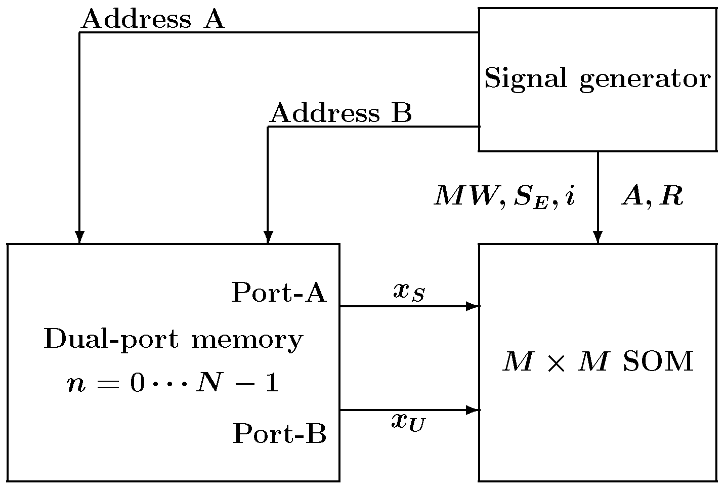
The experimental configuration for testing the SOM is shown in
Figure 10. The system consists of the proposed SOM, a signal generator, and dual-port memory, where
N is the number of training vectors. The entire system was written using VHDL for the FPGA implementation. The signal generator generates the necessary signals for the SOM to perform learning. The memory contains high-dimensional training vectors, and the dual-port memory is used for the pipeline computation. The precision of the vector elements in the memory was 8-bit while the weight vector elements stored in the neurons were represented by 16-bit fixed point format (8-bit integer and 8-bit fractional parts). The number of training iterations was 16 epochs, and the neighborhood function parameters
A and
R were implemented as follows:
where
E is number of epochs (
).
In the experiment, the clustering problem was applied to the SOMs. Clustering is a segmentation problem in which the objective is to gather similar data together. It can be extended to vector quantization, where a large data set can be downsized to a smaller set by substituting a prototype that represents the corresponding cluster instead of the data that belongs to the cluster. Image samples of handwritten digits taken from the Modified National Institute of Standards and Technology (MNIST) database [
27] were used as training data. Each sample is a
grayscale image, making the dimension of the vector
. The MNIST data set consists of ten classes of handwritten digits, and 100 samples were randomly taken from each class for training. The memory shown in
Figure 10 stores these training data, which is 1000 in total (
).
First, the nested SOM and flat SOM were described by VHDL and were processed by Quartus prime targeting Aria 10 FPGA. With clock constraints set to 20 ns (50 MHz), six implementations were performed with different strategies. The strategies in
Table 1 are provided by Quartus prime. A properly selected strategy optimizes the FPGA implementation in speed, area, or power consumption. The implementation results are summarized in
Table 1. The better results using the same strategy are highlighted in bold. The table shows that the nested architecture yielded faster and smaller hardware SOMs in five out of six strategies.
The same implementation experiment was carried out with AMD Vivado design tools. These tools are provided by the FPGA vendor, i.e., AMD, for users to develop their FPGA designs. Virtex-7 VC709 Evaluation Platform (xc7vx690tffg1761-2) was used for the implementation. We tested three different versions of Vivado (Vivado 2019, 2020, and 2021) for the implementations, using a 20 ns (50 MHz) clock constraint. The Vivado design tool does synthesis and implementation steps for the FPGA design. The synthesis is the process of transforming a register transfer level (RTL) design into a gate-level representation, and place-and-route the netlist onto the FPGA device resources is carried out in the implementation step. The synthesis and implementation steps include various strategies for optimizing speed, area, runtime, or power consumption. For the synthesis strategy, Flow_PerfOptimized_high, which optimizes the performance, was chosen. Since Vivado has many implementation strategies, 24 performance-related strategies were tested to find one that better fits SOM architecture.
The WNS was used to estimate the operation speed. Various constraints, such as clock period, are predefined to help the synthesis tools run efficiently. The tools do the PAR while trying to meet all constraints. The WNS is the difference between the target clock period that is defined in the constraint and the estimated clock period.
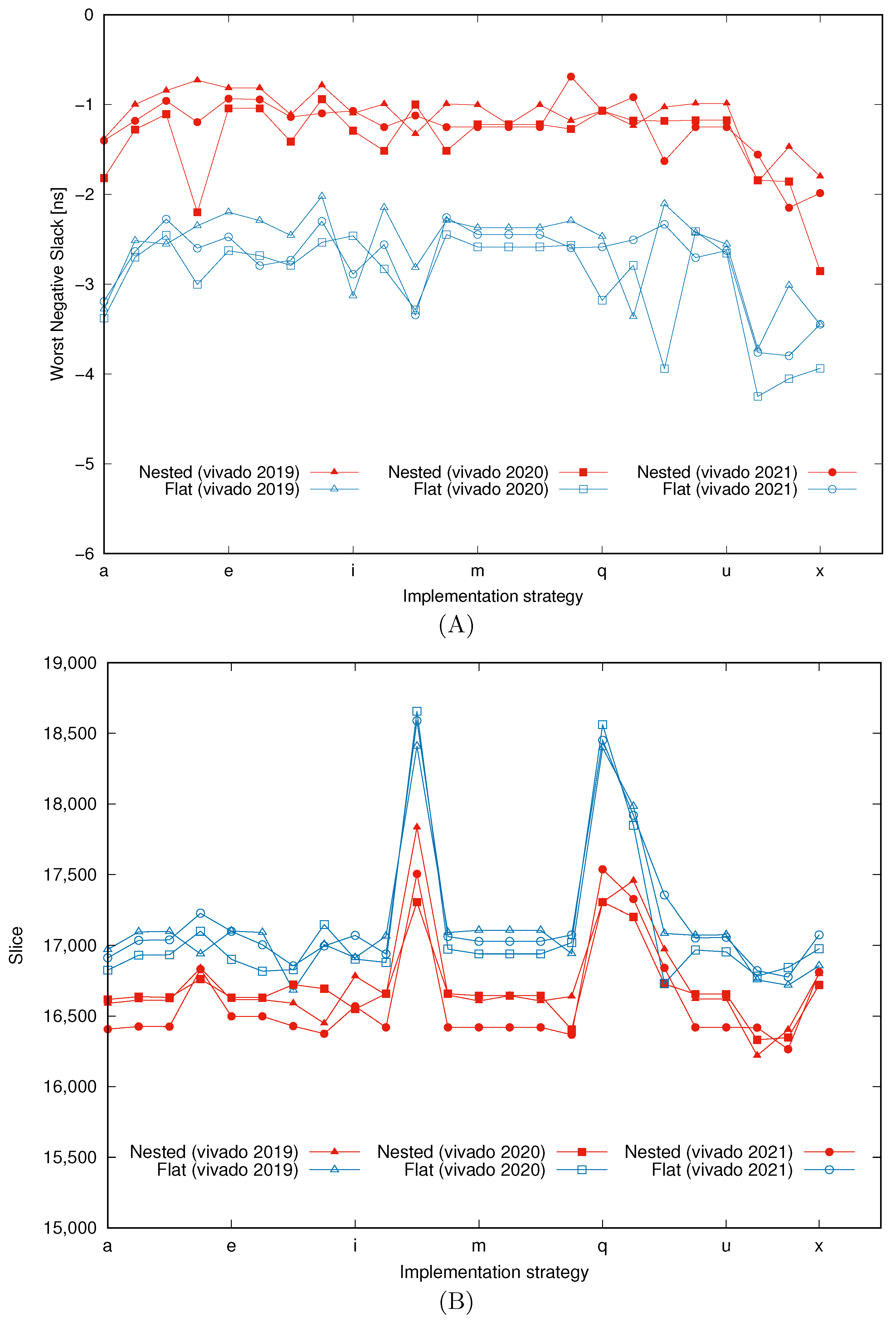
Figure 11A shows the WNS, where labels ‘a’ ∼ ‘x’ on the x-axis represent the implementation strategies. Positive WNS means that the implemented design’s clock period is less than the target period. Because all WNSs are negative, the closer the WNS is to zero, the higher clock frequency can be expected. This figure indicates that the speed of the circuit generated using the nested architecture was faster than that of the flat architecture for all implementation strategies.
Figure 11B shows the slice utilization of the implemented designs. Slice is a basic logic element included in FPGA and constitutes a configurable logic block. Each slice contains lookup tables (LUTs), registers, a feed chain, and multiplexers. The result revealed that the nested architecture produced a smaller design.
| a: Vivado Implementation Defaults, | b: Performance Explore, |
| c: Performance_ExplorePostRoutePhysOpt, | d: Performance_ExploreWithRemap, |
| e: Performance_WLBlockPlacement, | f: Performance_WLBlockPlacementFanoutOpt, |
| g: Performance_EarlyBlockPlacement, | h: Performance_NetDelay_high, |
| i: Performance_NetDelay_low, | j: Performance_Retiming, |
| k: Performance_ExtraTimingOpt, | l: Performance_RefinePlacement, |
| m: Performance_SpreadSLLs, | n: Performance_BalanceSLLs, |
| o: Performance_BalanceSLRs, | p: Performance_HighUtilSLRs, |
| q: Congestion_SpreadLogic_high, | r: Congestion_SpreadLogic_medium, |
| s: Congestion_SpreadLogic_low, | t: Congestion_SSI_SpreadLogic_high, |
| u: Congestion_SSI_SpreadLogic_low, | v: Area_Explore, |
| w: Area_ExploreSequential, | x: Area_ExploreWithRemap. |
Next, we experimentally examined the operable highest clock frequency. Using the top five strategies that performed well on each architecture with Vivado 2021 in
Figure 11, SOMs with two architectures were implemented on the FPGA, and operable clock frequencies were measured.
Table 2 summarizes the operating clock frequencies and slice usages of the two SOM architectures. The larger the WNS, the higher the operating clock frequency becomes, which improves the operating speed. In terms of the circuit size, a smaller number of slices is desired. The better results using the same strategy are highlighted in bold.
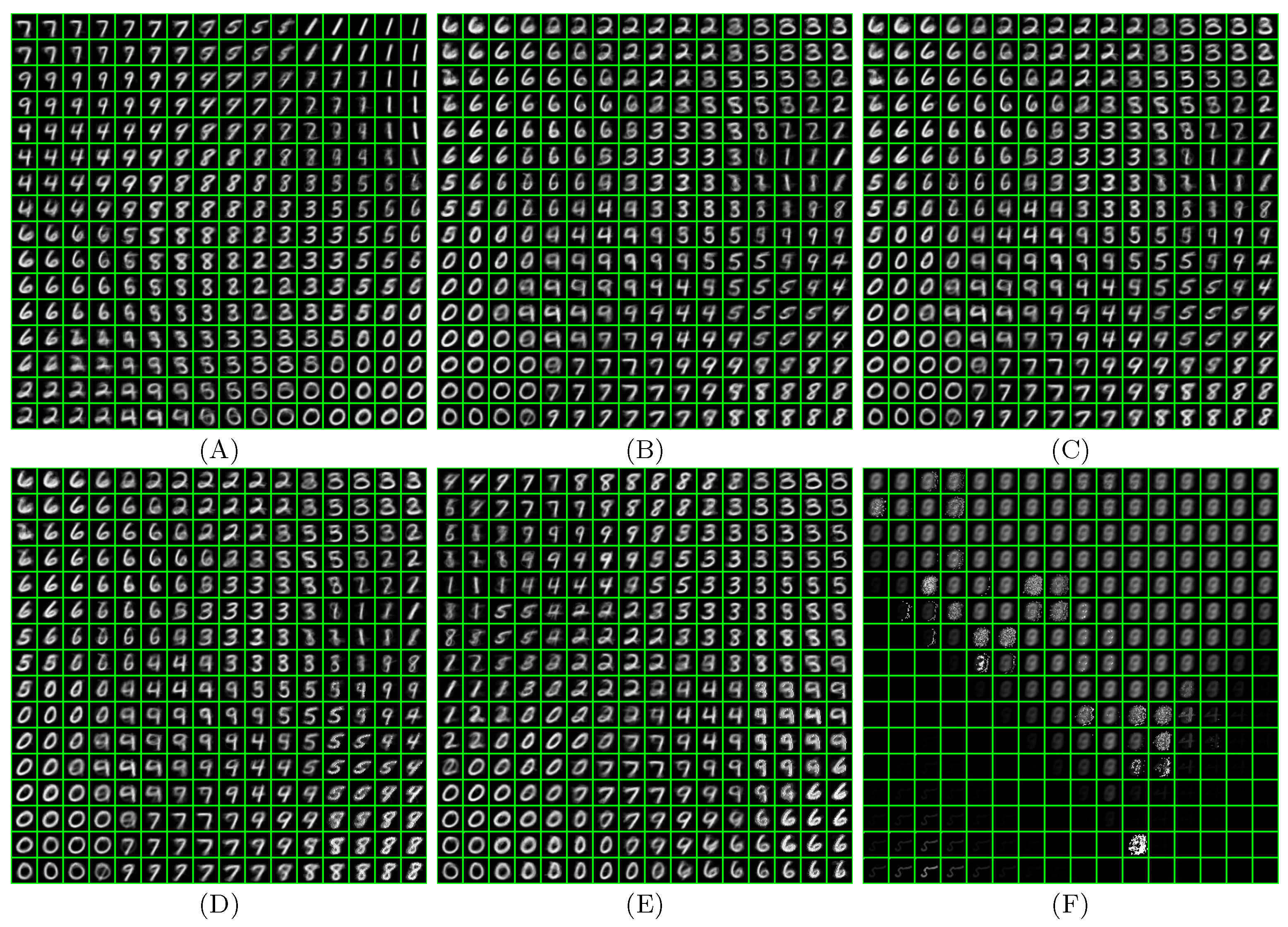
Figure 12 shows the neuron maps after training with different clock frequencies, as well as the maps generated by the software and VHDL simulations. The neuron map is a set of visualized weight vectors that were read out from the FPGA. Until the clock frequency reached 81 MHz, the generated maps and quantization errors were the same as those that the VHDL simulation generated, and a different map was generated at 82 MHz clock frequency. The diversity of the maps in the figure is likely due to calculation errors in the SOM circuit. Each computation circuit completes its calculation with a certain delay. Therefore, this delay must be less than the period of the clock signal. Otherwise, incorrect and incomplete calculation results will be output. For the 82 MHz clock, this timing violation appears to have occurred in the winner search circuit since the 82 MHz map is different from the 81 MHz map. Since the 83 MHz and 82 MHz maps are different, it is thought that the output results of the winner search circuit became unstable in this frequency range. Meanwhile, the vector update circuit seems to have worked correctly because the clear clustering can be observed in the map. Finally, the map collapsed at 88 MHz clock, as shown in
Figure 12F because the weight update circuit apparently failed to work. The map obtained with an 82 MHz clock shows the topology-preserving nature of the SOM, and its quantization error (QE) is the same level as that of the 81 MHz map, so the SOM appears to be operating at a clock frequency above 82 MHz. Hence, we need a criterion to determine the highest operable clock frequency. Here, the operating frequency was taken as the highest frequency that produced the same map as the VHDL simulation. Therefore, 81 MHz is the highest operable clock frequency in this case.
To further demonstrate the impact of the nested architecture, we implemented the nested and flat architecture SOMs on different FPGAs and compared the implementation results. The design tool processed the implementations for Virtex7, Virtex ultrascale, Kintex, Kintex ultrascale, and Zynq ultrascale FPGAs with the same constraints as the previous experiment. For synthesis and implementation strategies, Flow_PerfOptimized_high and Performance explore were used, respectively.
Table 3 summarizes the results, including WNS estimation, a lookup table (LUT), Elapsed time, and Total on-chip power estimation. For the hardware size estimation, we used the number of LUTs for the designs because some of the FPGAs are configured using a configurable logic block (CLB) instead of the Slice. Both the Slice and CLB contain the LUTs for the logic implementation. The Elapsed time is the amount of time for the tool to complete the implementation. We used a PC with an i9-12900K processor running at 3.19 GHz clock frequency. Same as the other tables, the better results are highlighted in bold. As this table shows, the nested architecture provided a smaller and faster design implementation with smaller power consumption while it required the tool to have a longer processing time.
6. Discussion
As
Table 2 indicates, the nested architecture resulted in a smaller and better performing SOM in all cases, even though flat architecture-friendly strategies were used. The highest clock frequency in
Table 2 is 81 MHz. The operating clock frequency of the previous research [
10] was 60 MHz, but the frequency has been improved by 20 MHz. This is thought to be due to improved pipeline processing. Embedded counter counted 12,617,184 clocks during the learning. Therefore, the training time can be calculated as 0.1558 s with 81 MHz clock frequency. The total number of vector element updates during the training was
, which translates to
vector elements were updated in one second. Since the connection update is equivalent to the vector elements update in the SOM, the 81 MHz clock frequency resulted in a learning rate of 21.61 giga connection updates per second (GCUPS).
Regarding the quantization error, the SOM implemented in the FPGA had the same quantization error at 10 MHz, but the error decreased at about 80 MHz. Since this phenomenon occurred in the higher frequency region, it is thought that small calculation errors within the circuit caused the reduction of the quantization error, as discussed before. As shown in
Figure 12A shows, the quantization error of software SOM is much smaller than that of hardware SOMs implemented on the FPGA. This is because the software SOM used floating-point calculations and a traditional Gaussian neighborhood function, while all variables in the hardware SOMs are integers.
Table 1,
Table 2 and
Table 3, and
Figure 11 clearly show that the nested architecture results in a faster and smaller design over the flat architecture. The advantage of the nested architecture is due to its structure, as both architectures incorporate the same pipeline computation. Here, from
Table 2, we examine more detailed implementation results for both architectures. The average values of the characteristics of both architectures are compared.
WNS (estimated performance)
Slice (resource utilization)
Clock freq. (physical performance)
The WNS is the estimated delay difference from clock constraints (20 ns). Thus, the smaller, the better. On average, the WNS of the nested architecture is only 38.2% of the WNS of the flat design. The number of slices indicates the size of the hardware design; thus, fewer slices are desired. The nested architecture’s slice usage is, on average, 97.2% of the flat design. The frequency of the clock determines the physical operating speed of the hardware SOM; thus, the clock frequency is more important than WNS. The comparison reveals that the nested architecture SOM can operate with 10% higher clock frequency compared to the flat SOM design.
Execution speeds of existing hardware SOMs in the literature are summarized in
Table 4. Due to the modification to the pipeline computation method in this paper, the performance of the SOM with the MNIST training vector reached 20.6 GCUPS, which is higher than its predecessor [
10] by 5 GCUPS. However, the clock frequency of the state-of-the-art SOM exceeds 100 MHz, which is much higher than this work. The proposed architecture made use of only temporal parallelism by the pipeline computing, but the SOM algorithm is made of independent tasks such as the vector distance computation and weight vector update. In addition, the vector distance computation and the vector update computation can be done with fewer clocks by processing multiple vector elements simultaneously. Therefore, the performance of the proposed architecture can be further improved by exploiting spatial parallelism, where multiple computing units are employed. For example, if the number of the vector distance computing unit and the weight update unit is four, the performance would be quadrupled. Since the cost of the spatial parallel architecture is very high, a novel implementation method would be required.


