
Relative Jitter Measurement Methodology and Comparison of Clocking Resources Jitter in Artix 7 FPGA


Abstract
:1. Introduction
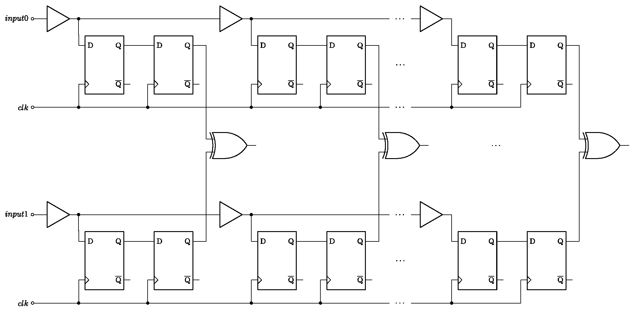
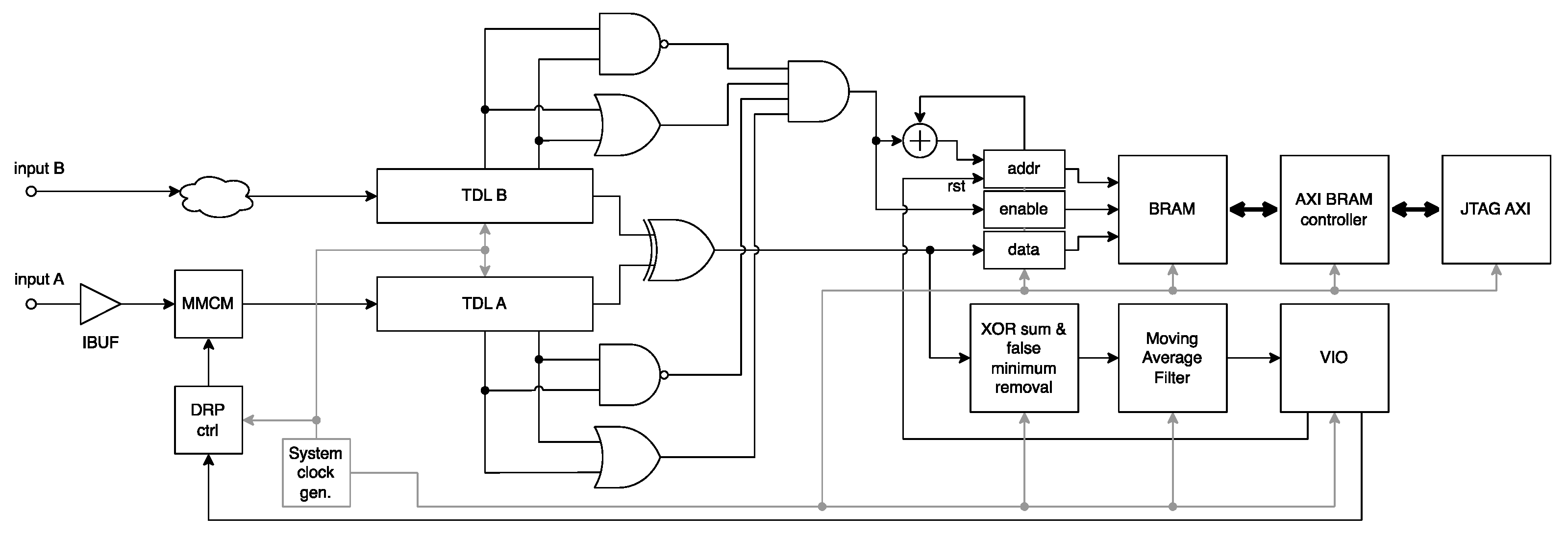
2. Design Architecture
2.1. Initial Concept
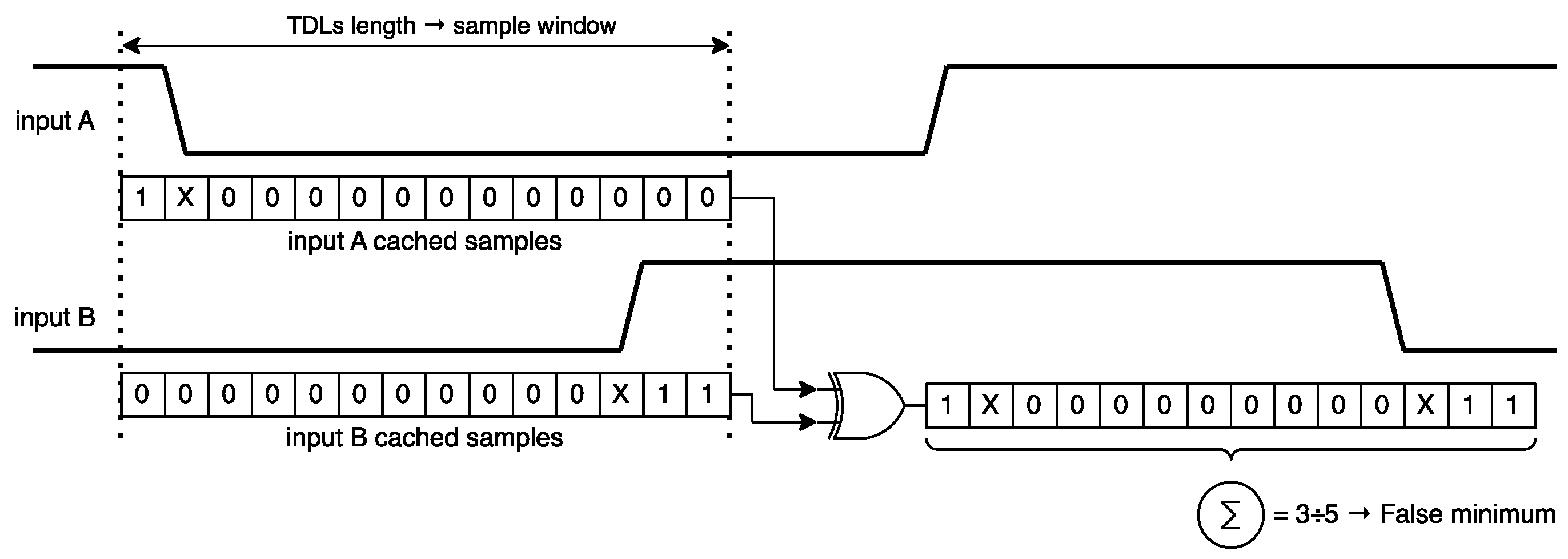
- No transition is detected in both TDLs for a certain amount of time;
- Multiple transitions are detected in the XORed difference of the two TDL vectors—as depicted in Figure 6.
3. Measurement Methodology
- Set the MMCM phase shift value (from 0 to 255) via the VIO and restart the MMCM;
- Read 16 average measurements (MA filter output values) via the VIO and calculate the final average for the currently selected MMCM phase shift value;
- After repeating the first and second step for all 256 phase shifts, set the MMCM phase shift equal to the value corresponding to the least average measurement acquired in Step 2;
- After resetting the BRAM via the VIO, wait for memory to fill up with data;
- Read the FPGA die temperature using a temperature sensor in the FPGA XADC (system monitor) [24];
- Read the BRAM data to the connected PC via the JTAG to the AXI Master;
- Repeat steps four through six fifty times and merge the acquired data and temperatures to two CSV files.
3.1. Calculation of Absolute Jitter
- The CARRY4 primitive delays reported by Xilinx Vivado are the same for all elements used for TDL implementation, but differ depending on the PVT corner—as depicted in Table 2;
- The reported delays for each CARRY4 primitive are non-monotonic—as depicted in Table 2;
- The interconnect delays between the consecutive CARRY4 elements reported by Xilinx Vivado are 0 (with 1 ps precision) for interconnects in a single clock region, and non-zero for interconnects across clock regions;
- While the paths from the system clock source to the corresponding TDL flip-flops are symmetrical (as described in Section 2.1), the delays for each flip-flop pair are different and non-monotonic—as depicted in Tables S1 and S2 in the Supplementary Materials;
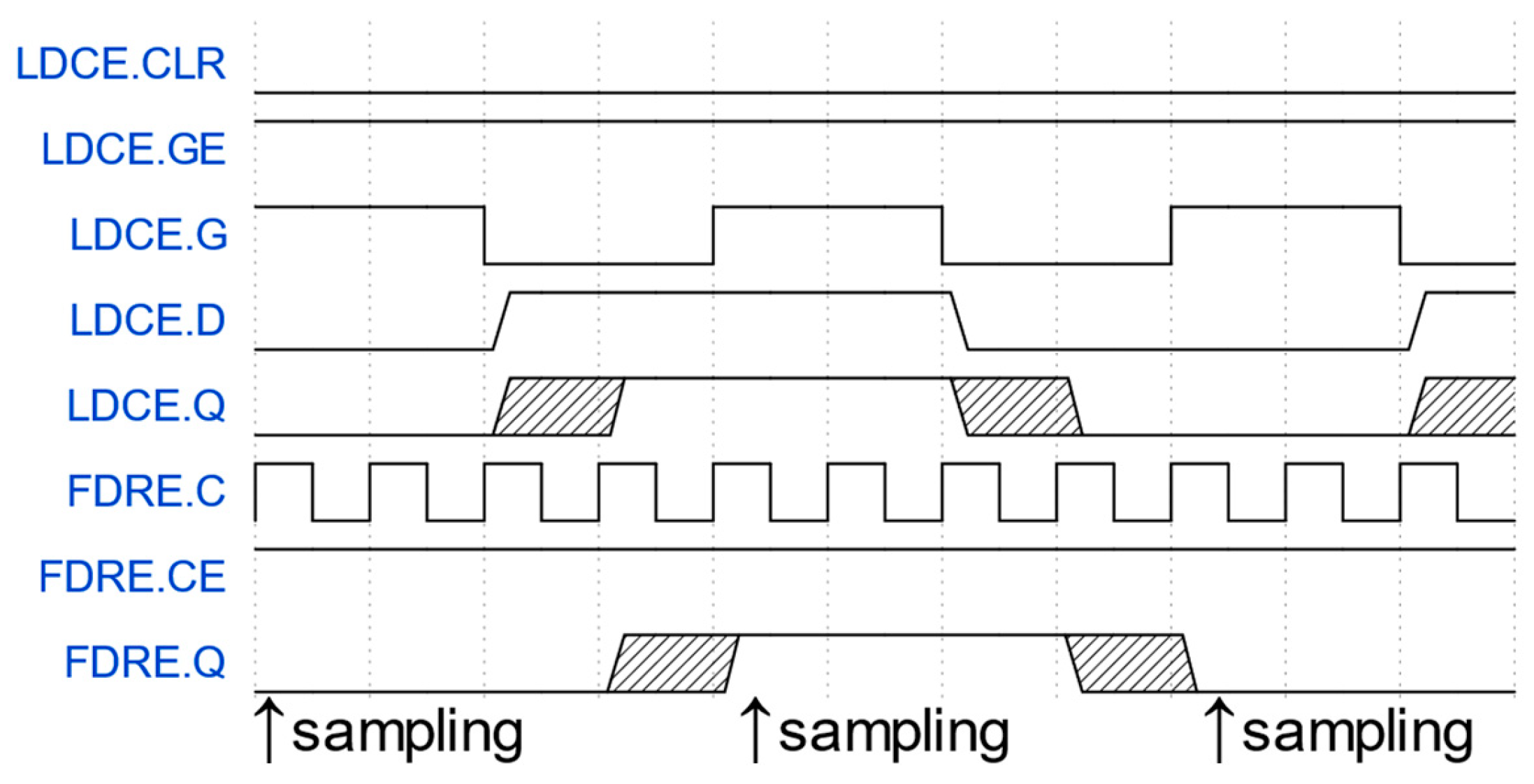
- The setup and hold time violations (resulting in storage elements metastability) are inherent to the TDL architecture, which is an additional source of Gaussian jitter [28] that would need to be subtracted from the raw measurement. This effect is further discussed in Section 4.1.
3.2. Relative Entropy Calculation
4. Reference Measurements and Initial Concept Revision
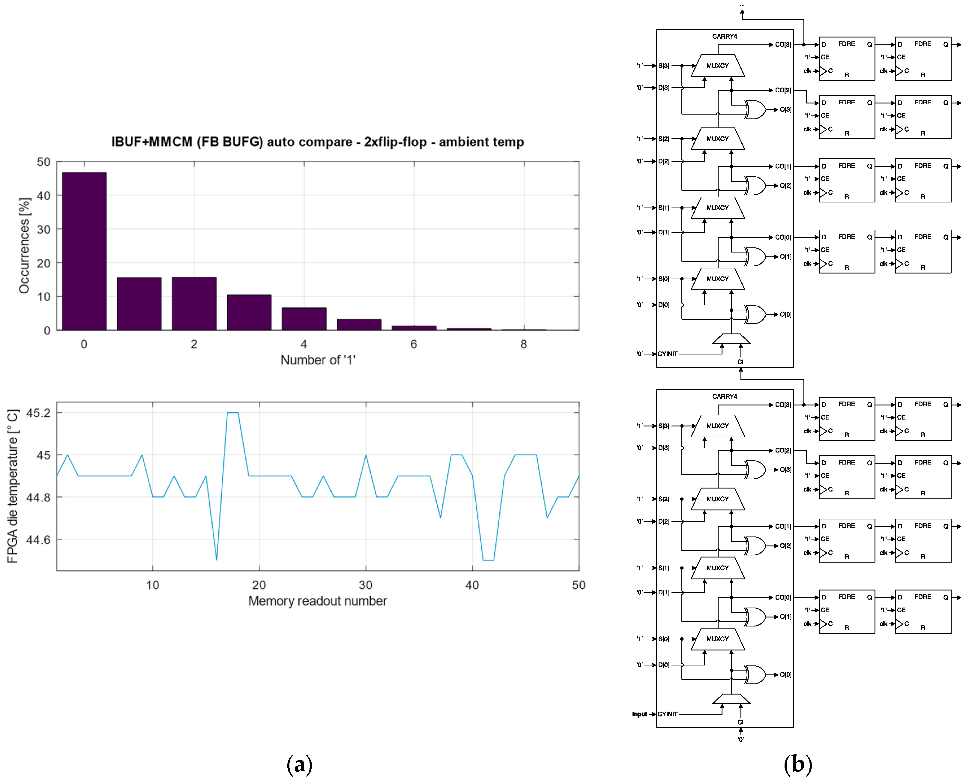
4.1. Design Verification
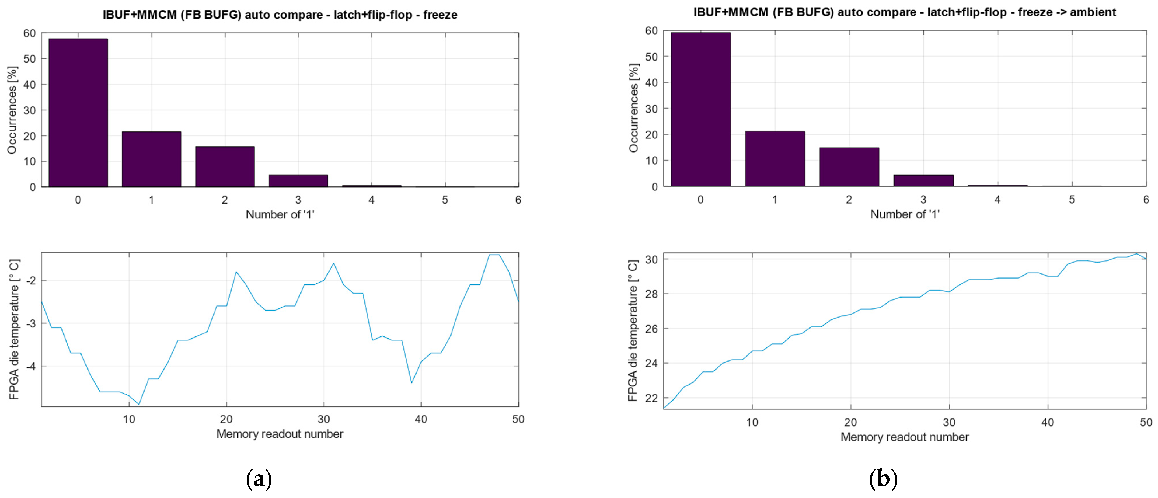
4.2. Temperature Influence
5. Results
- Involving a common input pin and a single common clock region for TDLs and both compared signal sources;
- Involving a common input pin and a separate clock region for TDLs with a reference signal source and a second clock region for a compared signal source;
- Involving a separate input pin and a single common clock region for TDLs and both compared signal sources;
- Involving a separate input pin (in common I/O bank) and a separate clock region for TDLs with a ref. signal source and second clock region for a compared signal source;
- Involving a separate input pin (in different I/O bank) and a separate clock region for TDLs with a ref. signal source and second clock region for a compared signal source.
5.1. Common Input Pin and Single Common Clock Region
5.2. Common Input Pin and a Separate Clock Region
5.3. Separate Input Pin in the Same Clock Region and a Single Common Clock Region
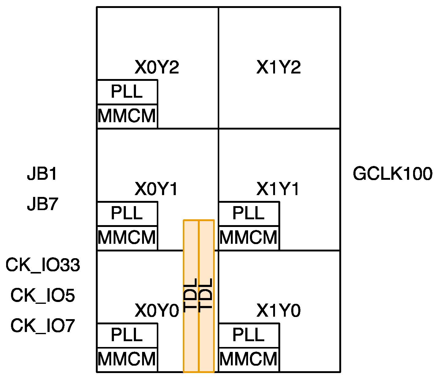
- Clock-capable T14 pin (named CK_IO5 in Arty A7 board),
- Clock-capable P15 pin (named CK_IO33 in Arty A7 board),
- Non-clock-capable T16 pin (named CK_IO7 in Arty A7 board).
5.4. Separate Input Pin (in Common I/O Bank) and a Separate Clock Region
5.5. Separate Input Pin (in Different I/O Bank) and a Separate Clock Region
- Clock-capable E15 pin (named JB1 in Arty A7 board),
- Non-clock-capable J17 pin (named JB7 in Arty A7 board).
5.6. Comparison of the Results
- Ideal theoretical PDF of 100% zero differences detected;
- Empirical PDF of auto compared latch+flip-flop configuration, stated in Section 4.1.

| Section/ Config. Number | Result Name | Relative Entropy (Ideal Ref.) | Relative Entropy (Empirical Ref.) |
|---|---|---|---|
| 4.1 | IBUF + MMCM auto compare—latch+flip-flop—ambient temp. | 5.15235 | 0 |
| 4.2 | IBUF + MMCM auto compare—latch+flip-flop—freeze -> ambient | 5.22654 | 0.000155105 |
| 4.2 | IBUF + MMCM auto compare—latch+flip-flop—freeze | 5.4275 | 0.00167469 |
| 5.5.1 | Sep. IBUF (CC X0Y1 pin) | 5.40074 | 0.602199 |
| 4.1 | IBUF + MMCM auto compare—2xflip-flop—ambient temp. | 6.62013 | 0.732354 |
| 5.5.9 | Sep. IBUF (nCC X0Y1 pin) + MMCM (X0Y1) + BUFG | 6.13525 | 0.7401 |
| 5.5.2 | Sep. IBUF (CC X0Y1 pin) + BUFG | 5.45964 | 0.818643 |
| 5.5.7 | Sep. IBUF (nCC X0Y1 pin) | 5.37273 | 0.989554 |
| 5.5.6 | Sep. IBUF (CC X0Y1 pin) + BUFG + PLL (X0Y1) + BUFG | 6.14203 | 1.07626 |
| 5.5.5 | Sep. IBUF (CC X0Y1 pin) + PLL (X0Y1) + BUFG | 6.2609 | 1.22945 |
| 5.4.2 | Sep. IBUF (CC X0Y0 pin) + BUFG + PLL (X0Y1) + BUFG | 6.28831 | 1.37145 |
| 5.3.10 | Sep. IBUF (nCC X0Y0 pin) + BUFG + PLL | 6.27178 | 1.42141 |
| 5.5.8 | Sep. IBUF (nCC X0Y1 pin) + BUFG | 5.6276 | 1.47346 |
| 5.3.4 | Sep. IBUF (CC X0Y0 pin) + BUFG + PLL | 6.27908 | 1.50762 |
| 5.3.7 | Sep. IBUF (nCC X0Y0 pin) | 5.67175 | 1.98895 |
| 5.5.11 | Sep. IBUF (nCC X0Y1 pin) + PLL (X0Y1) + BUFG | 6.41065 | 2.04863 |
| 5.1.1 | Com. IBUF | 5.66629 | 2.05207 |
| 5.5.12 | Sep. IBUF (nCC X0Y1 pin) + BUFG + PLL (X0Y1) + BUFG | 6.42639 | 2.10493 |
| 5.5.10 | Sep. IBUF (nCC X0Y1 pin) + BUFG + MMCM (X0Y1) + BUFG | 6.53075 | 2.11106 |
| 5.4.3 | Sep. IBUF (nCC X0Y0 pin) + BUFG + MMCM (X0Y1) + BUFG | 6.63287 | 2.28577 |
| 5.1.6 | Com. IBUF + PLL + BUFG | 6.56871 | 2.40495 |
| 5.3.6 | Sep. IBUF (CC X0Y0 pin) + BUFG + PLL + BUFG | 6.58761 | 2.94546 |
| 5.3.1 | Sep. IBUF (CC X0Y0 pin) | 5.56103 | 2.98708 |
| 5.3.3 | Sep. IBUF (CC X0Y0 pin) + PLL | 6.66421 | 3.00739 |
| 5.3.11 | Sep. IBUF (nCC X0Y0 pin) + PLL + BUFG | 6.8134 | 3.20675 |
| 5.3.8 | Sep. IBUF (nCC X0Y0 pin) + BUFG | 5.84805 | 3.30594 |
| 5.4.4 | Sep. IBUF (nCC X0Y0 pin) + BUFG + PLL (X0Y1) + BUFG | 6.63702 | 3.48722 |
| 5.4.1 | Sep. IBUF (CC X0Y0 pin) + BUFG + MMCM (X0Y1) + BUFG | 6.73066 | 3.52268 |
| 5.3.2 | Sep. IBUF (CC X0Y0 pin) + BUFG | 5.86949 | 3.79135 |
| 5.1.7 | Com. IBUF + BUFG + PLL | 6.7178 | 3.89694 |
| 5.5.4 | Sep. IBUF (CC X0Y1 pin) + BUFG + MMCM (X0Y1) + BUFG | 6.80247 | 4.36376 |
| 5.3.12 | Sep. IBUF (nCC X0Y0 pin) + BUFG + PLL + BUFG | 6.8181 | 4.65398 |
| 5.2.2 | Com. IBUF + BUFG + MMCM (X0Y1) + BUFG | 7.02862 | 5.37672 |
| 5.2.2 | Com. IBUF + BUFG + PLL (X0Y1) + BUFG | 6.8868 | 5.59853 |
| 5.1.2 | Com. IBUF + BUFG | 6.34482 | 5.75471 |
| 5.1.4 | IBUF + MMCM (FB BUFG)—OUTPUT1 + BUFG | 7.24451 | 5.79941 |
| 5.1.3 | IBUF + MMCM (FB BUFG)—OUTPUT1 | 7.26737 | 5.80405 |
| 5.1.8 | Com. IBUF + BUFG + PLL + BUFG | 7.12567 | 5.88812 |
| 5.3.9 | Sep. IBUF (nCC X0Y0 pin) + PLL | 7.12688 | 6.1222 |
| 5.3.5 | Sep. IBUF (CC X0Y0 pin) + PLL + BUFG | 7.20829 | 6.12283 |
| 5.5.3 | Sep. IBUF (CC X0Y1 pin) + MMCM (X0Y1) + BUFG | 7.15239 | 6.14977 |
| 5.1.5 | Com. IBUF + PLL | 7.17464 | 6.20072 |
6. Conclusions
- Common IBUF (configuration 5.1.1, relative entropy: 5.66629) vs. Common IBUF + BUFG (configuration 5.1.2, relative entropy: 5.75471);
- Separate clock-capable pin IBUF in X0Y0 region (configuration 5.3.1, relative entropy: 2.98708) vs. separate clock-capable pin IBUF in X0Y0 region + BUFG (configuration 5.3.2, relative entropy: 3.79135);
- Separate non-clock-capable pin IBUF in X0Y0 region (configuration 5.3.7, relative entropy: 1.98895) vs. separate non-clock-capable pin IBUF in X0Y0 region + BUFG (configuration 5.3.8, relative entropy: 3.30594);
- Separate clock-capable pin IBUF in X0Y1 region (configuration 5.5.1, relative entropy: 0.602199) vs. separate clock-capable pin IBUF in X0Y1 region + BUFG (configuration 5.5.2, relative entropy: 0.818643);
- Separate non-clock-capable pin IBUF in X0Y1 region (configuration 5.5.7, relative entropy: 0.989554) vs. separate non-clock-capable pin IBUF in X0Y1 region + BUFG (configuration 5.5.8, relative entropy: 1.47346).
- Separate clock-capable pin IBUF in X0Y0 region + BUFG + PLL (X0Y1) + BUFG (configuration 5.4.2, relative entropy: 1.37145) vs. separate clock-capable pin IBUF in X0Y0 region + BUFG + PLL (X0Y0) + BUFG (configuration 5.3.6, relative entropy: 2.94546);
- Separate non-clock-capable pin IBUF in X0Y0 region + BUFG + PLL (X0Y1) + BUFG (configuration 5.4.4, relative entropy: 3.48722) vs. separate non-clock-capable pin IBUF in X0Y0 region + BUFG + PLL (X0Y0) + BUFG (configuration: 5.3.12, relative entropy: 4.65398).
- Separate non-clock-capable pin IBUF in X0Y0 region + BUFG + PLL (X0Y0) (configuration 5.3.10, relative entropy: 1.42141) vs. separate non-clock-capable pin IBUF in X0Y0 region + PLL (X0Y0) + BUFG (configuration 5.3.9, relative entropy: 6.1222);
- Separate clock-capable pin IBUF in X0Y0 region + BUFG + PLL (X0Y0) (configuration 5.3.4, relative entropy: 1.50762) vs. separate clock-capable pin IBUF in X0Y0 region + PLL (X0Y0) + BUFG (configuration 5.3.3, relative entropy: 3.00739);
- Common IBUF (configuration 5.1.7, relative entropy: 3.89694) vs. common IBUF + BUFG (configuration 5.1.5, relative entropy: 6.20072);
- Separate clock-capable pin IBUF in X0Y1 region + BUFG + MMCM (X0Y1) + BUFG (configuration 5.5.4, relative entropy: 4.36376) vs. separate clock-capable pin IBUF in X0Y1 region + MMCM (X0Y1) + BUFG (configuration 5.5.3, relative entropy: 6.14977);
- Separate non-clock-capable pin IBUF in X0Y1 region + MMCM (X0Y1) + BUFG (configuration 5.5.9, relative entropy: 0.7401) vs. separate non-clock-capable pin IBUF in X0Y1 region + BUFG + MMCM (X0Y1) + BUFG (configuration 5.5.10, relative entropy: 2.11106);
- Separate clock-capable pin IBUF in X0Y1 region + BUFG + PLL (X0Y1) + BUFG (configuration 5.5.6, relative entropy: 1.07626) vs. separate clock-capable pin IBUF in X0Y1 region + PLL (X0Y1) + BUFG (configuration 5.5.5, relative entropy: 1.22945);
- Separate non-clock-capable pin IBUF in X0Y1 region + PLL (X0Y1) + BUFG (configuration 5.5.11, relative entropy: 2.04863) vs. separate non-clock-capable pin IBUF in X0Y1 region + BUFG + PLL (X0Y1) + BUFG (configuration 5.5.12, relative entropy: 2.10493).
- Separate clock-capable pin IBUF in X0Y0 region + BUFG + PLL (X0Y0) (configuration 5.3.4, relative entropy: 1.50762) vs. separate clock-capable pin IBUF in X0Y0 region + BUFG + PLL (X0Y0) + BUFG (configuration 5.3.6, relative entropy: 2.94546);
- Separate clock-capable pin IBUF in X0Y0 region + PLL (X0Y0) (configuration 5.3.3, relative entropy: 3.00739) vs. separate clock-capable pin IBUF in X0Y0 region + PLL (X0Y0) + BUFG (configuration 5.3.5, relative entropy: 6.12283);
- Separate non-clock-capable pin IBUF in X0Y0 region + BUFG + PLL (X0Y0) (configuration 5.3.10, relative entropy: 1.42141) vs. separate non-clock-capable pin IBUF in X0Y0 region + BUFG + PLL (X0Y0) + BUFG (configuration 5.3.12, relative entropy: 4.65398);
- Separate non-clock-capable pin IBUF in X0Y0 region + PLL (X0Y0) + BUFG (configuration 5.3.11, relative entropy: 3.20675) vs. separate non-clock-capable pin IBUF in X0Y0 region + PLL (X0Y0) (configuration 5.3.9, relative entropy: 6.1222);
- Common IBUF + BUFG + PLL (X0Y0) (configuration 5.1.7, relative entropy: 3.89694) vs. Common IBUF + BUFG + PLL (X0Y0) + BUFG (configuration 5.1.8, relative entropy: 5.88812);
- Common IBUF + PLL (X0Y0) + BUFG (configuration 5.1.6, relative entropy: 2.40495) vs. Common IBUF + PLL (X0Y0) (configuration 5.1.5, relative entropy: 6.20072);
- Separate MMCM output + BUFG (configuration 5.1.4, relative entropy: 5.79941) vs. Separate MMCM output (configuration 5.1.3, relative entropy: 5.80405).
Supplementary Materials
Author Contributions
Funding
Data Availability Statement
Conflicts of Interest
References
- Zamek, I.; OnWong, M.; Boyle, P.; Daud, N.; Soh, L.N.; Teng, H.L.; Fong, C.S. A study of jitter effects in nm-FPGA based on various physical and electrical quantities. In Proceedings of the 2007 Asia-Pacific Conference on Applied Electromagnetics, Melaka, Malaysia, 4–6 December 2007. [Google Scholar]
- Kho, J.; Loh, C.I.; Moo, W.H.; Fong, C.S.; Wong, M.O. Extended analysis of SSN effect on phase-locked loop (PLL) circuit. In Proceedings of the 2009 IEEE Electrical Design of Advanced Packaging & Systems Symposium (EDAPS), Hong Kong, China, 2–4 December 2009; pp. 1–4. [Google Scholar]
- Teng, H.L.; Sun, S.; Wong, M.O.; Boyle, P.; Fong, C.S. A study of the relationship between on-chip power distribution network voltage noise, charge per clock cycle, on-chip decoupling capacitance and clock jitter in a 40-nm field programmable gate array test chip. In Proceedings of the 2010 International Conference on Applications of Electromagnetism and Student Innovation Competition Awards (AEM2C), Taipei, Taiwan, 11–13 August 2010; pp. 75–79. [Google Scholar]
- Aloisio, A.; Giordano, R.; Izzo, V. Jitter issues in clock conditioning with FPGAs. In Proceedings of the 2010 17th IEEE-NPSS Real Time Conference, Lisbon, Portugal, 24–28 May 2010. [Google Scholar]
- Borgosz, J. “Follow Me”—Digital Jitter Measurement Method. Meas. Sci. Rev. 2006, 6, 30–33. [Google Scholar]
- Xilinx Inc. Digital Clock Manager (DCM) Module Data Sheet (DS485); Xilinx Inc.: San Jose, CA, USA, 2009. [Google Scholar]
- Marins, C.N.M.; Kaufmann, P.; Júnior, A.A.F.; Paiva, M.; Swart, J.W. New Jitter Measurement Technique Using TDC Principle in a FPGA Component. In Proceedings of the Seminário Internacional de Metrologia Elétrica—VIII SEMETRO, João Pessoa, Brazil, 17–19 June 2009. [Google Scholar]
- Kubíček, M. In-system jitter measurement using FPGA. In Proceedings of the 20th International Conference Radioelektronika 2010, Brno, Czech Republic, 19–21 April 2010. [Google Scholar]
- Szplet, R.; Czuba, A. Two-Stage Clock-Free Time-to-Digital Converter Based on Vernier and Tapped Delay Lines in FPGA Device. Electronics 2021, 10, 2190. [Google Scholar] [CrossRef]
- Digilent. Arty A7. Available online: https://digilent.com/reference/programmable-logic/arty-a7/start (accessed on 5 July 2023).
- Xilinx Inc. Extending 28 nm Leadership with an Expanded Portfolio and Lower Power; Xilinx Inc.: San Jose, CA, USA, 2015. [Google Scholar]
- Wojciechowski, A.A.; Marcinek, K.; Pleskacz, W.A. Dual TDL Based Phase Difference Detector Architecture. In Proceedings of the 2023 30th International Conference on Mixed Design of Integrated Circuits and System (MIXDES), Kraków, Poland, 29–30 June 2023. [Google Scholar]
- Sui, T.; Zhao, Z.; Xie, S.; Xie, Y.; Zhao, Y.; Huang, Q.; Xu, J.; Peng, Q. A 2.3-ps RMS Resolution Time-to-Digital Converter Implemented in a Low-Cost Cyclone V FPGA. IEEE Trans. Instrum. Meas. 2019, 68, 3647–3660. [Google Scholar] [CrossRef] [PubMed]
- Dikopoulos, E.; Birbas, M.; Birbas, A. An Adaptive Downsampling FPGA-Based TDC Implementation for Time Measurement Improvement. Chips 2022, 1, 175–190. [Google Scholar] [CrossRef]
- Tontini, A.; Gasparini, L.; Pancheri, L.; Passerone, R. Design and characterization of a low-cost FPGA-based TDC. IEEE Trans. Nucl. Sci. 2018, 65, 680–690. [Google Scholar] [CrossRef]
- Xilinx Inc. 7 Series FPGAs Configurable Logic Block User Guide (UG474); Xilinx Inc.: San Jose, CA, USA, 2016. [Google Scholar]
- Xilinx Inc. Vivado Design Suite 7 Series FPGA and Zynq 7000 SoC Libraries Guide (UG953); Xilinx Inc.: San Jose, CA, USA, 2023. [Google Scholar]
- Xilinx Inc. Block Memory Generator v8.4 Product Guide (PG058); Xilinx Inc.: San Jose, CA, USA, 2021. [Google Scholar]
- Xilinx Inc. AXI Block RAM (BRAM) Controller v4.1 Product Guide (PG078); Xilinx Inc.: San Jose, CA, USA, 2019. [Google Scholar]
- Xilinx Inc. JTAG to AXI Master v1.2 Product Guide (PG174); Xilinx Inc.: San Jose, CA, USA, 2021. [Google Scholar]
- Al-Mbaideen, A.A. Application of Moving Average Filter for the Quantitative Analysis of the NIR Spectra. J. Anal. Chem. 2019, 74, 686–692. [Google Scholar] [CrossRef]
- Xilinx Inc. Virtual Input/Output v3.0 Product Guide (PG159); Xilinx Inc.: San Jose, CA, USA, 2018. [Google Scholar]
- Tatsukawa, J. MMCM and PLL Dynamic Reconfiguration Application Note v1.8 (XAPP888); Xilinx Inc.: San Jose, CA, USA, 2019. [Google Scholar]
- Xilinx Inc. 7 Series FPGAs and Zynq-7000 SoC XADC Dual 12-Bit 1 MSPS Analog-to-Digital Converter User Guide (UG480); Xilinx Inc.: San Jose, CA, USA, 2022. [Google Scholar]
- Silicon Laboratories. Si5351A/B/C; Silicon Laboratories: Austin, TX, USA, 2011. [Google Scholar]
- Skyworks Solutions Inc. Understanding and Optimizing Clock Buffer’s Additive Jitter Performance (AN766); Skyworks Solutions Inc.: Irvine, CA, USA, 2021. [Google Scholar]
- Gardner, F.M. Phaselock Techniques, 3rd ed.; John Wiley & Sons, Inc.: Hoboken, NJ, USA, 2005. [Google Scholar]
- Serra, P.C.; Conklin, J.W. On-Chip System for Fast, High-Range, High-Precision Measurements of Delays. IEEE Trans. Instrum. Meas. 2020, 69, 5243–5250. [Google Scholar] [CrossRef]
- Kullback, S.; Leibler, R.A. On information and sufficiency. Ann. Math. Stat. 1951, 22, 79–86. [Google Scholar] [CrossRef]
- Wieczorek, P.Z. Dual-metastability FPGA-based true random number generator. Electron. Lett. 2013, 49, 744–745. [Google Scholar] [CrossRef]
- Xilinx Inc. Artix-7 FPGAs Data Sheet: DC and AC Switching Characteristics (DS181); Xilinx Inc.: San Jose, CA, USA, 2022. [Google Scholar]
- Yoshikawa, K.; Kanamaru, K.; Inui, S.; Hagihara, Y.; Nakamura, Y.; Yoshimura, Y. Timing optimization by replacing flip-flops to latches. In Proceedings of the ASP-DAC 2004: Asia and South Pacific Design Automation Conference 2004 (IEEE Cat. No.04EX753), Yokohama, Japan, 27–30 January 2004; pp. 186–191. [Google Scholar]
- Vasumathi, S.P.; Murlidharan, D. A survey on flip flop replacement to latch on various design. Int. J. Pure Appl. Math. 2018, 119, 13453–13467. [Google Scholar]
- Chinnery, D.; Keutzer, K. Reducing the Timing Overhead. In Closing the Gap Between ASIC & Custom: Tools and Techniques for High-Performance ASIC Design; Springer: Boston, MA, USA, 2002; pp. 57–100. [Google Scholar]
- Mao, X.; Yang, F.; Wei, F.; Shi, J.; Cai, J.; Cai, H. A Low Temperature Coefficient Time-to-Digital Converter with 1.3 ps Resolution Implemented in a 28 nm FPGA. Sensors 2022, 22, 2306. [Google Scholar] [CrossRef] [PubMed]
- Yan, C.; Hu, C.; Wu, J. A High Resolution Vernier Digital-to-Time Converter Implemented with 65 nm FPGA. Appl. Sci. 2019, 9, 2705. [Google Scholar] [CrossRef]
- Bosco, K.J.; Pavalam, S.M.; Mpamije, L.J. Fundamental Flip-Flop Design: Comparative Analysis. J. VLSI Circuits Syst. 2023, 5, 1–7. [Google Scholar]
- Xilinx Inc. 7 Series FPGAs Clocking Resources User Guide (UG472); Xilinx Inc.: San Jose, CA, USA, 2018. [Google Scholar]

| Resource | Utilization | Available | Utilization % |
|---|---|---|---|
| LUT | 3116 | 20,800 | 14.98% |
| LUTRAM | 372 | 9600 | 3.88% |
| FF | 4442 | 41,600 | 10.68% |
| BRAM | 44 | 50 | 88% |
| DSP | 0 | 90 | 0% |
| CARRY4 Input | CARRY4 Output | FAST_MAX Corner | FAST_MIN Corner | SLOW_MAX Corner | SLOW_MIN Corner |
|---|---|---|---|---|---|
| CYINIT | CO0 | 206 ps | 165 ps | 536 ps | 432 ps |
| CYINIT | CO1 | 180 ps | 144 ps | 494 ps | 398 ps |
| CYINIT | CO2 | 210 ps | 169 ps | 592 ps | 477 ps |
| CYINIT | CO3 | 215 ps | 173 ps | 580 ps | 467 ps |
| CIN | CO0 | 100 ps | 76 ps | 271 ps | 206 ps |
| CIN | CO1 | 56 ps | 45 ps | 157 ps | 127 ps |
| CIN | CO2 | 81 ps | 65 ps | 228 ps | 184 ps |
| CIN | CO3 | 49 ps | 39 ps | 114 ps | 92 ps |
| Number of ‘1s’ | 2x Flip-Flop Configuration | Latch + Flip-Flop Configuration |
|---|---|---|
| 0 | 46.682% | 59.646% |
| 1 | 15.561% | 20.775% |
| 2 | 15.658% | 14.968% |
| 3 | 10.456% | 4.194% |
| 4 | 6.604% | 0.415% |
| 5 | 3.192% | 0.001% |
| 6 | 1.188% | 0.000% |
| 7 | 0.502% | 0.000% |
| 8 | 0.158% | 0.000% |
| 9 | 0.000% | 0.000% |
| CARRY4 Element Index | CARRY4 Element Output | Accumulated Delay | Setup Time Violation | Hold Time Violation |
|---|---|---|---|---|
| 0 | CO0 | 76 ps | ✓ | ✓ |
| CO1 | 45 ps | ✓ | ✓ | |
| CO2 | 65 ps | ✓ | ✓ | |
| CO3 | 39 ps | ✓ | ✓ | |
| 1 | CO0 | 115 ps | ✗ | ✓ |
| CO1 | 84 ps | ✓ | ✓ | |
| CO2 | 104 ps | ✓ | ✓ | |
| CO3 | 78 ps | ✓ | ✓ | |
| 2 | CO0 | 154 ps | ✗ | ✓ |
| CO1 | 123 ps | ✗ | ✓ | |
| CO2 | 143 ps | ✗ | ✓ | |
| CO3 | 117 ps | ✗ | ✓ | |
| 3 | CO0 | 193 ps | ✗ | ✓ |
| CO1 | 162 ps | ✗ | ✓ | |
| CO2 | 182 ps | ✗ | ✓ | |
| CO3 | 156 ps | ✗ | ✓ | |
| 4 | CO0 | 232 ps | ✗ | ✗ |
| CO1 | 201 ps | ✗ | ✓ | |
| CO2 | 221 ps | ✗ | ✗ | |
| CO3 | 195 ps | ✗ | ✓ |
| Number of ‘1s’ | Ambient Temperature <42.8 °C; 43.2 °C> | Freezing Temperature <−4.9 °C; −1.4 °C> | Heating Up from Freezing Temperature <21.4 °C; 30.3 °C> |
|---|---|---|---|
| 0 | 59.646% | 57.697% | 59.130% |
| 1 | 20.775% | 21.491% | 21.155% |
| 2 | 14.968% | 15.648% | 14.910% |
| 3 | 4.194% | 4.640% | 4.397% |
| 4 | 0.415% | 0.510% | 0.406% |
| 5 | 0.001% | 0.0137% | 0.001% |
| 6 | 0.000% | 0.000% | 0.000% |
| Config. Number | Config. Name | Schematic Diagram and Short Summary | Measurement Results at Ambient Temperature |
|---|---|---|---|
| 5.1.1 | Common IBUF | 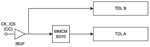 | 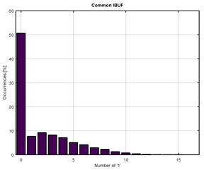 |
| |||
| 5.1.2 | Common IBUF + BUFG |  | 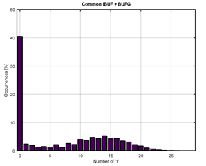 |
| |||
| 5.1.3 | Separate MMCM output | 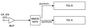 | 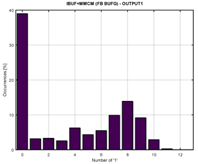 |
| |||
| 5.1.4 | Separate MMCM output + BUFG | 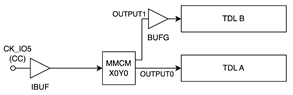 | 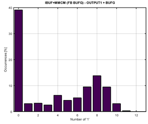 |
| |||
| 5.1.5 | Common IBUF + same clock region PLL | 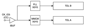 | 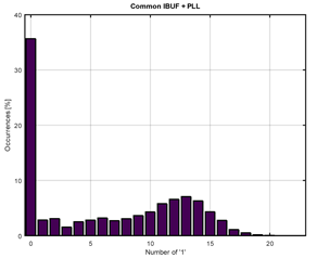 |
| |||
| 5.1.6 | Common IBUF + same clock region PLL + BUFG | 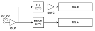 | 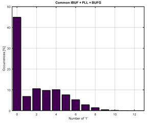 |
| |||
| 5.1.7 | Common IBUF + BUFG + same clock region PLL | 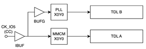 | 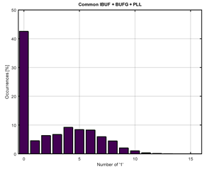 |
| |||
| 5.1.8 | Common IBUF + BUFG + same clock region PLL + BUFG | 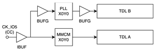 | 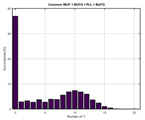 |
|
| Config. Number | Config. Name | Schematic Diagram and Short Summary | Measurement Results at Ambient Temperature |
|---|---|---|---|
| 5.2.1 | Common IBUF + BUFG + separate clock region MMCM + BUFG | 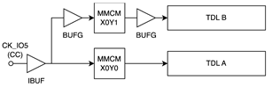 | 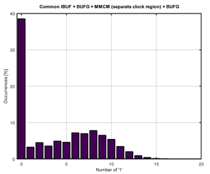 |
| |||
| 5.2.2 | Common IBUF + BUFG + separate clock region PLL + BUFG | 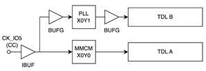 | 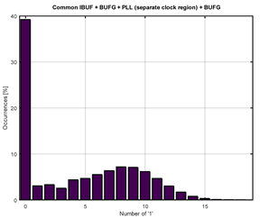 |
|
| Config. Number | Config. Name | Schematic Diagram and Short Summary | Measurement Results at Ambient Temperature |
|---|---|---|---|
| 5.3.1 | Separate IBUF (clock-capable pin in the same clock region) | 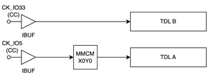 | 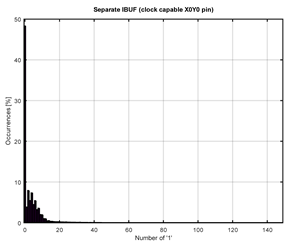 |
| |||
| 5.3.2 | Separate IBUF (clock-capable pin in the same clock region) + BUFG | 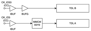 | 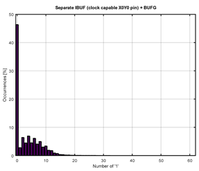 |
| |||
| 5.3.3 | Separate IBUF (clock-capable pin in the same clock region) + same clock region PLL | 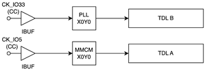 | 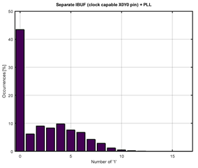 |
| |||
| 5.3.4 | Separate IBUF (clock-capable pin in the same clock region) + BUFG + same clock region PLL | 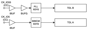 | 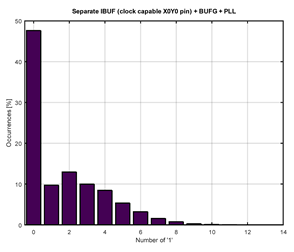 |
| |||
| 5.3.5 | Separate IBUF (clock-capable pin in the same clock region) + same clock region PLL + BUFG | 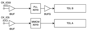 | 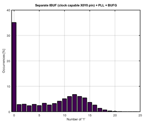 |
| |||
| 5.3.6 | Separate IBUF (clock-capable pin in the same clock region) + BUFG + same clock region PLL + BUFG | 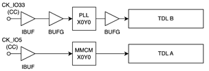 | 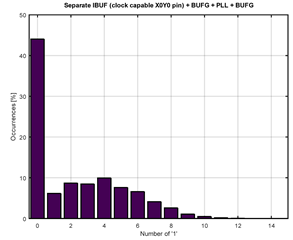 |
| |||
| 5.3.7 | Separate IBUF (non-clock-capable pin in the same clock region) | 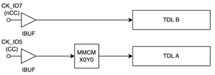 | 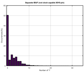 |
| |||
| 5.3.8 | Separate IBUF (non-clock-capable pin in the same clock region) + BUFG | 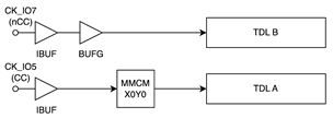 | 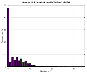 |
| |||
| 5.3.9 | Separate IBUF (non-clock-capable pin in the same clock region) + same clock region PLL | 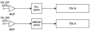 | 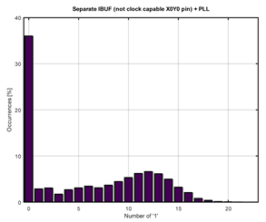 |
| |||
| 5.3.10 | Separate IBUF (non-clock-capable pin in the same clock region) + BUFG + same clock region PLL | 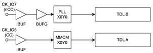 | 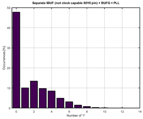 |
| |||
| 5.3.11 | Separate IBUF (non-clock-capable pin in the same clock region) + same clock region PLL + BUFG | 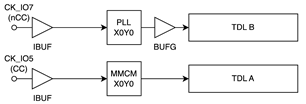 | 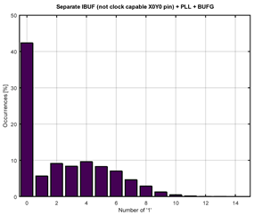 |
| |||
| 5.3.12 | Separate IBUF (non-clock-capable pin in the same clock region) + BUFG + same clock region PLL + BUFG | 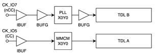 | 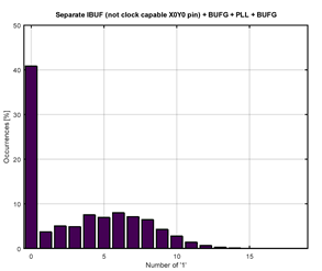 |
|
| Config. Number | Config. Name | Schematic Diagram and Short Summary | Measurement Results at Ambient Temperature |
|---|---|---|---|
| 5.4.1 | Separate IBUF (clock-capable pin in the same clock region) + BUFG + different clock region MMCM + BUFG | 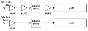 | 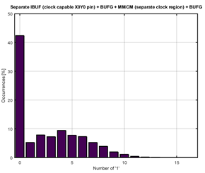 |
| |||
| 5.4.2 | Separate IBUF (clock-capable pin in the same clock region) + BUFG + different clock region PLL + BUFG | 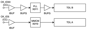 | 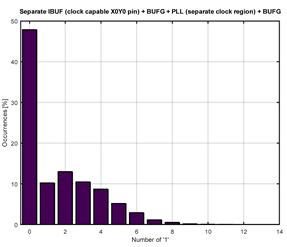 |
| |||
| 5.4.3 | Separate IBUF (non-clock-capable pin in the same clock region) + BUFG + different clock region MMCM + BUFG | 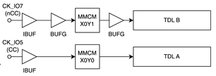 | 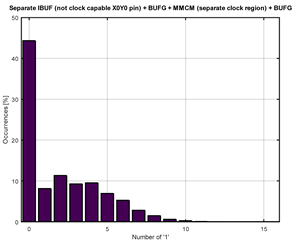 |
| |||
| 5.4.4 | Separate IBUF (non-clock-capable pin in the same clock region) + BUFG + different clock region PLL + BUFG | 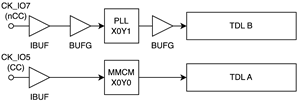 | 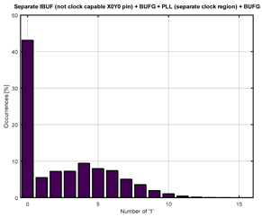 |
|
| Config. Number | Config. Name | Schematic Diagram and Short Summary | Measurement Results at Ambient Temperature |
|---|---|---|---|
| 5.5.1 | Separate IBUF (clock-capable pin in X0Y1 clock region) | 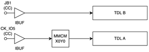 | 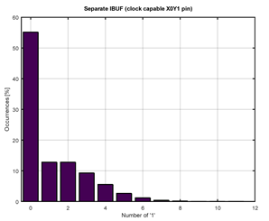 |
| |||
| 5.5.2 | Separate IBUF (clock-capable pin in X0Y1 clock region) + BUFG | 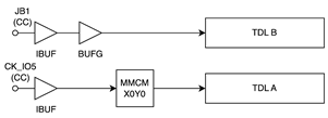 | 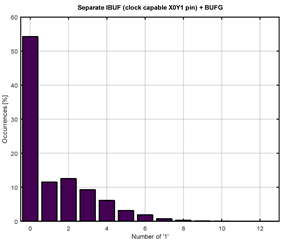 |
| |||
| 5.5.3 | Separate IBUF (clock-capable pin in X0Y1 clock region) + X0Y1 clock region MMCM + BUFG | 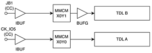 | 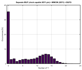 |
| |||
| 5.5.4 | Separate IBUF (clock-capable pin in X0Y1 clock region) + BUFG + X0Y1 clock region MMCM + BUFG | 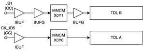 | 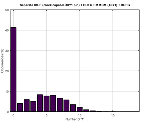 |
| |||
| 5.5.5 | Separate IBUF (clock-capable pin in X0Y1 clock region) + X0Y1 region PLL + BUFG |  | 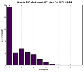 |
| |||
| 5.5.6 | Separate IBUF (clock-capable pin in X0Y1 clock region) + BUFG + X0Y1 clock region PLL + BUFG | 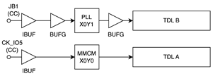 | 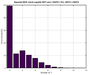 |
| |||
| 5.5.7 | Separate IBUF (non-clock-capable pin in X0Y1 clock region) | 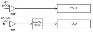 | 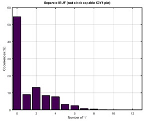 |
| |||
| 5.5.8 | Separate IBUF (non-clock-capable pin in X0Y1 clock region) + BUFG | 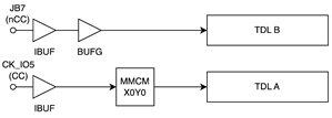 | 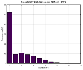 |
| |||
| 5.5.9 | Separate IBUF (non-clock-capable pin in X0Y1 clock region) + X0Y1 clock region MMCM + BUFG | 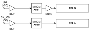 | 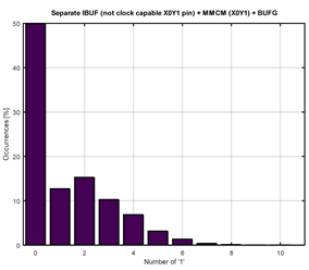 |
| |||
| 5.5.10 | Separate IBUF (non-clock-capable pin in X0Y1 clock region) + BUFG + X0Y1 clock region MMCM + BUFG | 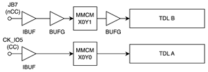 | 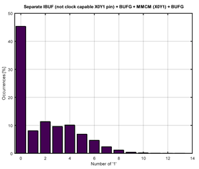 |
| |||
| 5.5.11 | Separate IBUF (non-clock-capable pin in X0Y1 clock region) + X0Y1 clock region PLL + BUFG | 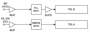 | 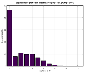 |
| |||
| 5.5.12 | Separate IBUF (non-clock-capable pin in X0Y1 clock region) + BUFG + X0Y1 clock region PLL + BUFG | 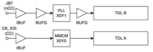 | 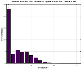 |
|
Disclaimer/Publisher’s Note: The statements, opinions and data contained in all publications are solely those of the individual author(s) and contributor(s) and not of MDPI and/or the editor(s). MDPI and/or the editor(s) disclaim responsibility for any injury to people or property resulting from any ideas, methods, instructions or products referred to in the content. |
© 2023 by the authors. Licensee MDPI, Basel, Switzerland. This article is an open access article distributed under the terms and conditions of the Creative Commons Attribution (CC BY) license (https://creativecommons.org/licenses/by/4.0/).
Share and Cite
Wojciechowski, A.A.; Marcinek, K.; Pleskacz, W.A. Relative Jitter Measurement Methodology and Comparison of Clocking Resources Jitter in Artix 7 FPGA. Electronics 2023, 12, 4297. https://doi.org/10.3390/electronics12204297
Wojciechowski AA, Marcinek K, Pleskacz WA. Relative Jitter Measurement Methodology and Comparison of Clocking Resources Jitter in Artix 7 FPGA. Electronics. 2023; 12(20):4297. https://doi.org/10.3390/electronics12204297
Chicago/Turabian StyleWojciechowski, Andrzej A., Krzysztof Marcinek, and Witold A. Pleskacz. 2023. "Relative Jitter Measurement Methodology and Comparison of Clocking Resources Jitter in Artix 7 FPGA" Electronics 12, no. 20: 4297. https://doi.org/10.3390/electronics12204297
APA StyleWojciechowski, A. A., Marcinek, K., & Pleskacz, W. A. (2023). Relative Jitter Measurement Methodology and Comparison of Clocking Resources Jitter in Artix 7 FPGA. Electronics, 12(20), 4297. https://doi.org/10.3390/electronics12204297