Article

Design and Implementation of Low-Power IoT RISC-V Processor with Hybrid Encryption Accelerator

School of Physical and Electronic Sciences, Changsha University of Science and Technology, Changsha 410114, China
*
Author to whom correspondence should be addressed.
Electronics 2023, 12(20), 4222; https://doi.org/10.3390/electronics12204222
Submission received: 11 September 2023 / Revised: 6 October 2023 / Accepted: 10 October 2023 / Published: 12 October 2023

Abstract

:
The security and reliability of data transmission between IoT devices are considered to be major challenges in the development of IoT technology. This paper presents a low-power, low-cost RISC-V processor for IoT applications with an integrated hybrid encryption accelerator, which can achieve efficient and secure encryption and decryption of data transmitted between IoT devices. The hybrid encryption accelerator, which uses the SM3 and the SM4, respectively, as hash and symmetric encryption algorithms, achieves a balance between encryption security, high speed, and key-management convenience. Both the processor and encryption accelerator are designed using the Verilog HDL language and are subsequently implemented and evaluated on both FPGA and ASIC platforms. The performance of the proposed processor and that of the Hummingbird E203 and the XuanTie E902 are compared. It is shown that, on the FPGA platform, the total resource utilization rate is reduced by 39.1~66.2%. In a 90 nm CMOS process, it is shown that the power efficiency of the proposed processor is increased by 10~34.8% and the circuit area is reduced by 32.5~57.1%.

1. Introduction

In recent years, the rapid evolution of the Internet of Things (IoT) has seen widespread integration of IoT devices across diverse domains, including smart homes, smart cities, healthcare, agriculture, and industries. Data communication between IoT devices has become more frequent, and meanwhile, data protection has become a critical issue [1]. Data transmitted over the network are vulnerable to eavesdropping and tampering, which compromise data quality and safety [2]. In this context, the imperative of our IoT era is to delve into strategies for ensuring robust data security.
Encryption and decryption serve as fundamental techniques underpinning data security and communication. The primary classifications of encryption algorithms encompass symmetric-key encryption, asymmetric-key encryption, and hash functions [3]. Symmetric-key encryption uses the same key for both encryption and decryption. Notable instances of symmetric-key encryption algorithms encompass AES [4] and SM4 [5]. Asymmetric-key encryption uses different keys for encryption and decryption. Some examples of asymmetric-key encryption algorithms are RSA [6] and SM2 [7]. Hash functions represent one-way mechanisms mapping input data to a fixed-length output, facilitating the verification of data integrity and authenticity. Eminent illustrations of hash function algorithms encompass MD5 [8] and SHA-2 [9]. Symmetric-key encryption offers rapidity and simplicity; its deployment necessitates a secure mechanism for key sharing between a sender and receiver. Conversely, asymmetric-key encryption, offering heightened security and flexibility, entails a trade-off in terms of reduced speed and heightened complexity compared to symmetric-key encryption. Hash functions excel at verifying data integrity and authenticity, but they lack the capacity for data encryption or decryption.
Hybrid encryption technology represents a versatile approach that integrates diverse encryption systems and algorithms, facilitating the creation of encryption schemes tailored to specific requirements. This technology substantiates enhancements in the security, efficiency, and convenience of encryption, decryption, and key management processes, consequently eliciting substantial attention in research and analysis. Li et al. proposed a novel hybrid encryption algorithm by using the initial encryption algorithm, the Micro Genard encryption algorithm, and the Base64 encryption algorithm. They enhance and optimize established encryption algorithms and meticulously reassemble them in a strategic sequence to bolster information security [10]. Shende et al. combined the advantages of AES and RSA algorithms to propose a hybrid encryption scheme that reduces complex calculations and increases computation speed without compromising the randomness and efficiency of the algorithm [11]. Chandu et al. proposed a hybrid encryption algorithm, using AES to encrypt the data generated by edge devices and RSA to encrypt the AES key, and implemented the design on FPGA to ensure data integrity and confidentiality [12]. Hui et al. introduced a real-time analysis and hybrid encryption technique for substantial data, leveraging Spark Streaming to fuse ECC encryption with block data encryption. Their approach encompassed a key generation method amalgamating semiconductor noise sources and chaotic sequences [13]. Zheng et al. devised a hybrid cryptographic framework for intelligent devices, entailing software/hardware co-design and integrating SM2/SM3/SM4 algorithms, thereby achieving a cost-effective, high-performance solution surpassing prior endeavors, and execution speed increased by over 10% [14]. Li et al. proposed an original triple-hybrid encryption system for a real-time sensitive image acquisition chip. This encryption system optimizes the symmetric encryption algorithm AES, asymmetric encryption algorithm ECC, and chip authentication algorithm PUF in pursuit of security; AES reduced the hardware area by 60.1%, and ECC reduced the hardware area by 43.4% [15]. However, prevailing hybrid encryption systems often rely on conventional processor architectures, with their acceleration units mostly attached to the CPU’s bus as peripherals, failing to fully exploit the flexibility and scalability inherent in the RISC-V instruction set. However, prevailing hybrid encryption systems often rely on conventional processor architectures, with their acceleration units mostly attached to the CPU’s bus as peripherals, failing to fully utilize the flexibility and scalability inherent in the RISC-V instruction set. This may result in data transmission delays and bandwidth limitations, increasing system power consumption, and this discrepancy leads to suboptimal alignment with IoT scenarios.
This paper presents a hybrid encryption scheme based on the SM3 and SM4 algorithms, both of which are Chinese national cryptographic standards, the former being a hash function and the latter a symmetric-key block cipher. The SM3 algorithm offers robust security and favorable performance when compared to other hash functions like SHA-256. Similarly, the SM4 algorithm boasts high security levels and cost-effectiveness in hardware, distinguishing it from block ciphers such as AES. Our hybrid encryption scheme is seamlessly integrated into a 32-bit, low-power IoT RISC-V processor, delivering notable efficiency, security, and data encryption flexibility. The processor core features a two-stage pipeline and supports RISC-V’s I and M standard extensions. Additionally, the hybrid encryption accelerator is seamlessly incorporated into the execution stage of the RISC-V processor, activated by custom instructions. To validate our approach, we assessed the processor core’s performance on an FPGA platform and conducted synthesis using 90 nm CMOS ASIC technology. The results clearly demonstrate the superiority of our design in terms of throughput, area utilization, and power efficiency when compared to existing alternatives.
The remainder of this paper is structured as follows. Section 2 provides an introduction to the foundational concepts of the RISC-V instruction set and the encryption algorithm. In Section 3, we delve into the architecture of the proposed processor and its constituent elements. Section 4 outlines the implementation results and offers an analysis of the proposed processor’s performance. Finally, Section 5 concludes the paper, offering insights into future avenues of research.

2. Background

2.1. SM3 Algorithm

The SM3 algorithm is a cryptographic hash function that can map any input data to fixed-length output data, called a message digest, which can be used for data encryption and integrity verification [16]. It was developed by the State Cryptography Administration of China and became a national standard in 2012 [17]. It is similar to SHA-256 in terms of security and efficiency [18]. The SM3 algorithm consists of three parts: message padding, message expansion, and a compression function [19]. For a plaintext message with a length of m bits, the SM3 algorithm performs a series of message padding and iterative compression operations, which finally produces a 256-bit hash value. The process is typically implemented in three steps as follows:
(1)
Message padding. Firstly, the plain message m is padded with a single bit “1” followed by k bits “0” ( l + 1 + k 448   m o d   512 ) and a 64-bit string, which is the binary representation of the message length. After padding, the length of the final padded message is a multiple of 512.
(2)
Message expansion. The padded message m is then divided into several 512-bit message blocks as B ( 0 ) , B ( 1 ) , , B ( n 1 ) . Each message block B ( i ) will be transformed into 132 words as W 0 , W 1 , , W 67 , W 0 , W 1 , , W 63 using the following method:
  • The message block B ( i ) is divided into 16 words W 0 , W 1 , , W 15 .
  • W j is calculated by:
    f o r   j = 16   t o   67 W j = P 1 ( W j 16 W j 9 ( W j 3 < < < 15 ) ) ( W j 13 < < < 7 ) W j 16 e n d f o r
    Here, P 1 ( · ) is a permutation function.
  • W j is calculated by:
    f o r   j = 0   t o   67 W j = W j W j + 4 e n d f o r
(3)
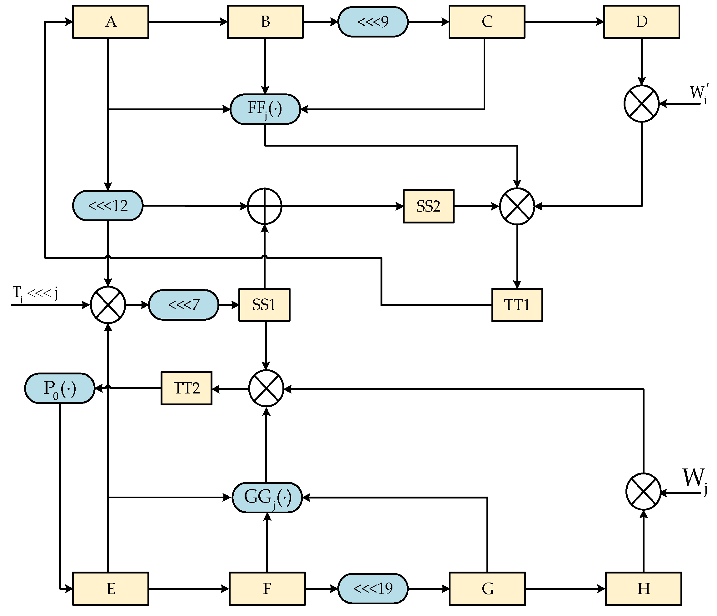
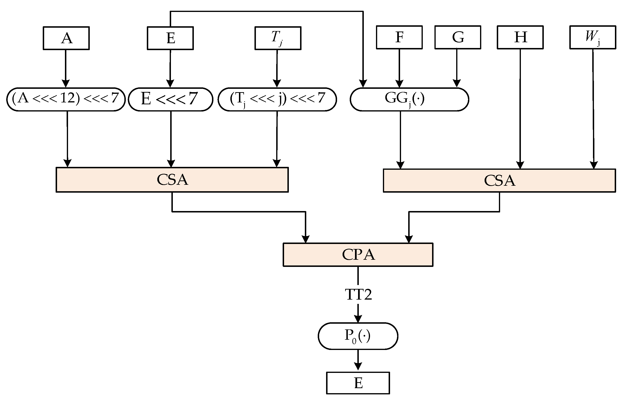
Message compression. Then, the message block B ( i ) is processed by:
V ( i + 1 ) = C F ( V ( i ) , B ( i ) ) ,   0 i n - 1
where C F is the compression function. V ( 0 ) is the initial value I V of the compression function, which is a 256-bit constant as defined in the algorithm standard. The operation procedure of the compression function C F can be summarized as follows:
A B C D E F G H = V ( i )
f o r   j = 0   t o   63 S S 1 = ( ( A < < < 12 ) + E + ( T j < < < j ) ) < < < 7 S S 2 = S S 1 ( A < < < 12 ) T T 1 = F F j ( A , B , C ) + D + S S 2 + W j T T 2 = G G j ( E , F , G ) + H + S S 1 + W j D = C C = B < < < 9 B = A A = T T 1 H = G G = F < < < 9 F = E E = P 0 ( T T 2 ) e n d f o r
V ( i + 1 ) = A B C D E F G H V ( i )
where A , B , C , D , E , F , G , and H are a 32-bit word. S S 1 , S S 2 , T T 1 , and T T 2 are intermediate variables. T j is a constant. F F j ( · ) and G G j ( · ) are Boolean functions. P 0 ( · ) is a permutation function. The final 256-bit hash value is:
A B C D E F G H = V ( n )
y = A B C D E F G H

2.2. SM4 Algorithm

The SM4 algorithm serves as a symmetric block cipher, adept at both data encryption and decryption, employing a 128-bit key and a 128-bit block size [20]. It was conceived by the State Cryptography Administration of China and was officially established as a national standard in 2012 [21]. Its widespread application encompasses data encryption and the fortification of wireless network security [22]. Structurally, the SM4 algorithm comprises three distinct stages: message padding, message expansion, and iterative compression [23]. The message padding phase introduces additional bits to the input message, aligning it to a multiple of 128 bits. Following this, the message expansion phase generates 32 round keys from the initial key, employing a non-linear function along with two constants. Lastly, the iterative compression phase enacts 32 encryption or decryption rounds on each 128-bit block of the padded message. This operation is facilitated using the round keys and a substitution-permutation network. Each round’s computation adheres to the following formula:
X i + 4 = X i T ( X i X i + 1 X i + 2 X i + 3 r k i )
where X i is a 32-bit word, represents the bitwise XOR operation, r k i is the round key for the i-th round, and T ( · ) is a non-linear transformation function that consists of an S-box and a linear transformation. The S-box is based on the multiplicative inverse over G F ( 2 8 ) with an affine transform. The linear transformation is defined by:
L ( B ) = B ( B < < < 2 ) ( B < < < 10 ) ( B < < < 18 ) ( B < < < 24 )
where B is a 32-bit word and < < < represents the cyclic left shift operation. The final output of the SM4 algorithm is a 128-bit cipher-text.

2.3. RISC-V Instruction Set

RISC-V is an instruction-set architecture that originated at the University of California, Berkeley, and it holds notable distinctions from the ×86 and ARM architectures [24]. Specifically, the RISC-V architecture offers a spectrum of benefits encompassing simplicity, flexibility, and considerable scalability. This architectural framework has gained significant traction within the realm of IoT devices [25]. RISC-V’s foundation rests on a modular design, enabling straightforward customization through the selection of diverse modules that align with varying application demands. Notably, this modular approach augments the system’s flexibility and scalability, consequently enhancing the overall architecture [26].
The basic instruction set in RISC-V is denoted by I, which is the subset of instructions that all processors need to support [27]. And the extension instruction sets can be selected according to specific application requirements. The basic instruction set provides the most essential functions, while the extension instruction sets provide more options and optimizations. In addition, RISC-V also supports user-defined instructions and reserves a significant amount of encoding space for custom instructions, which makes it easy to design custom instructions for domain-specific accelerators [28]. This flexible instruction set design makes RISC-V a versatile and adaptable architecture that can meet various application needs, while also promoting innovation and customization.

3. Hardware Implementation

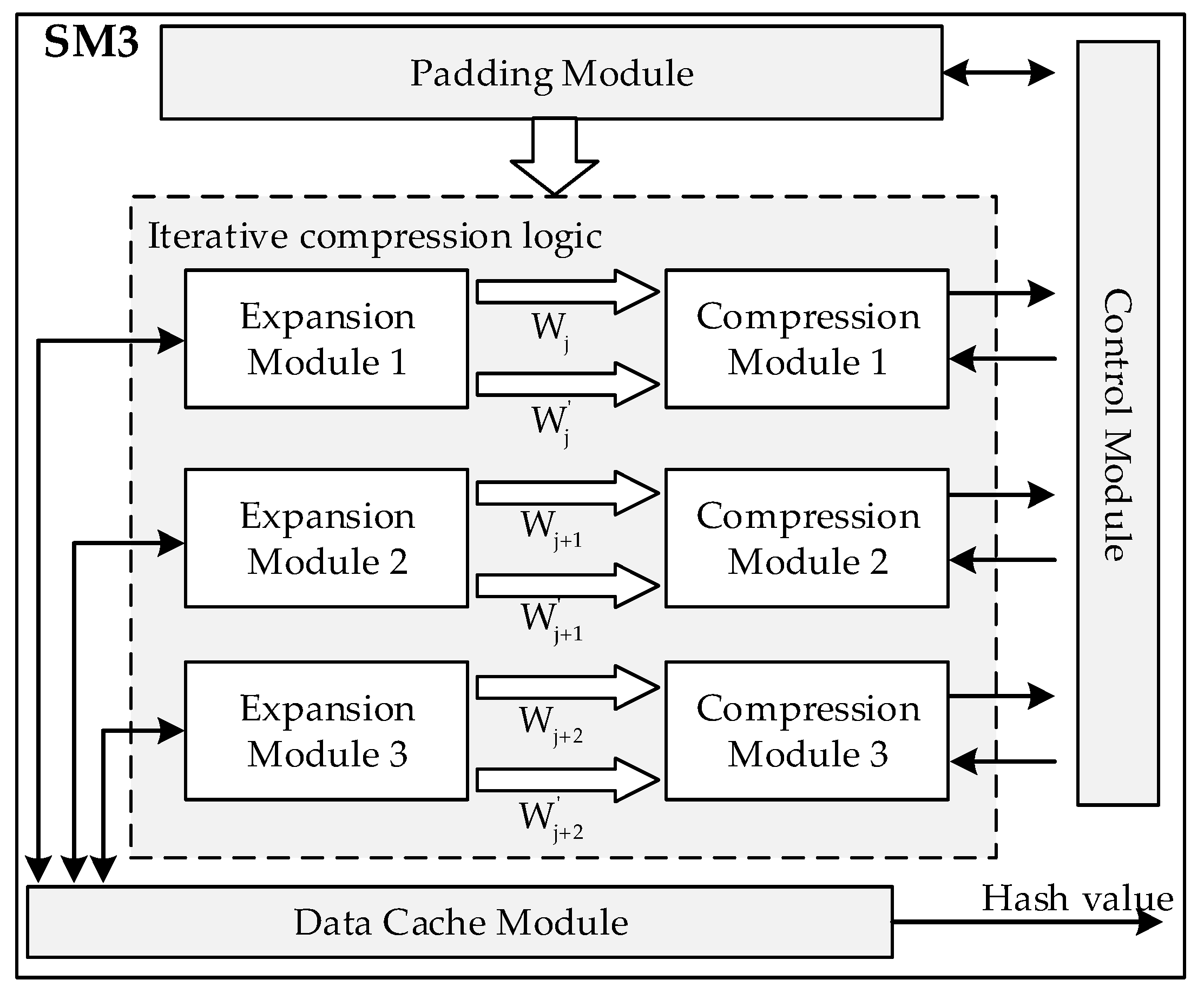
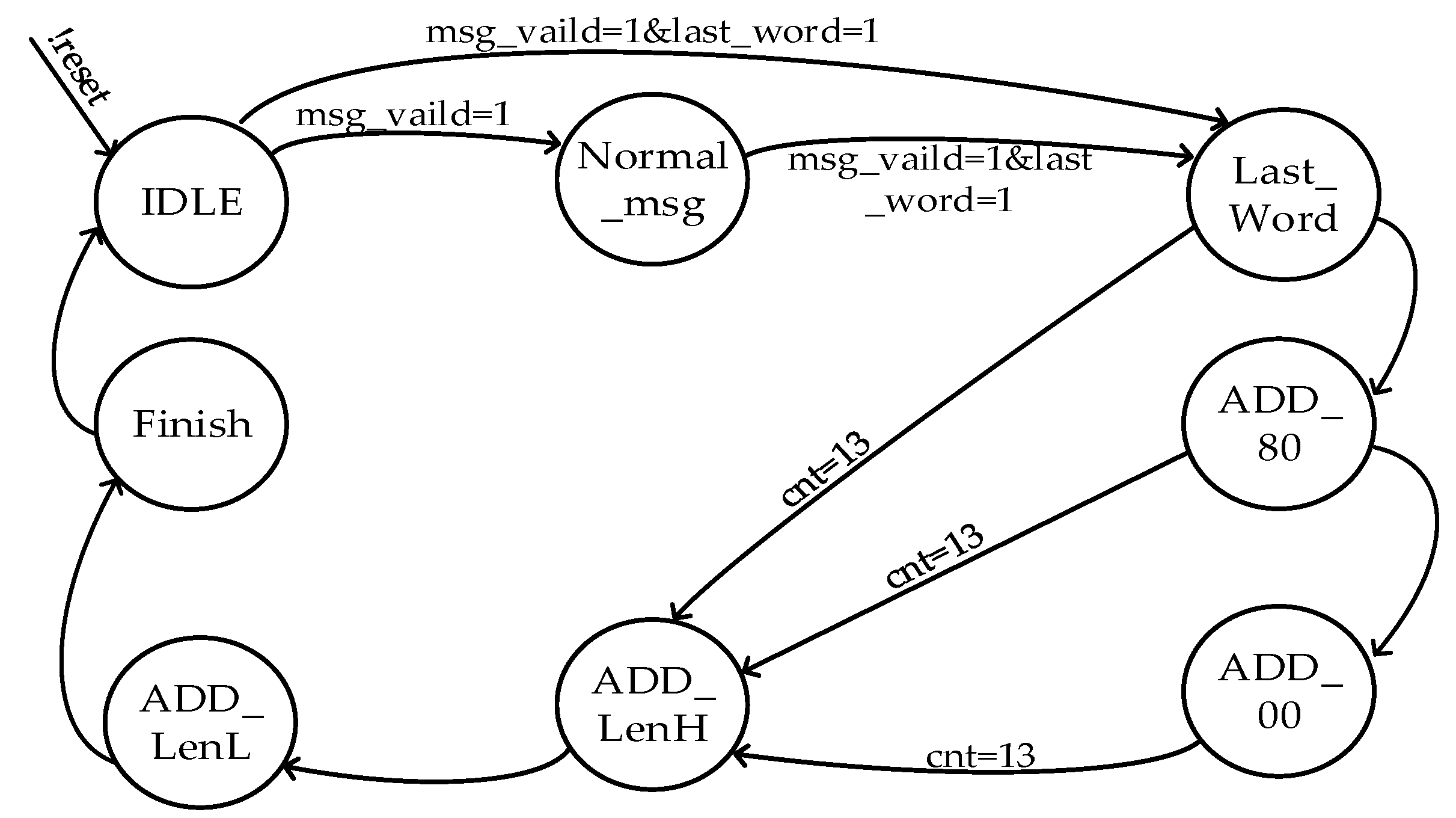
3.1. SM3 Algorithm Accelerator

The SM3 algorithm accelerator is a hardware circuit that can perform the SM3 algorithm faster and more efficiently than the software implementations. It consists of four parts: a message padding module, a control module, iterative compression logic, and a data cache module. From the previous section, the iterative compression process requires 64 rounds of computation. We use a three-way parallel computation scheme for the expansion and compression modules to improve the speed of encryption operation with low resource cost. Figure 1 shows the overall architecture of an SM3 algorithm accelerator. After a message padding operation, the plain message m is transformed into the padded message m , which is then sent to the iterative compression logic. Under the control of the control module, three expansion modules generate expansion words in parallel in each clock cycle and send them to the compression module. The compression module performs a round of compression calculations. After 22 clock cycles, the data cache module produces a 256-bit hash value. In our design, by using the hardware SM3 accelerator, high performance and low power consumption for data encryption can be achieved.
As depicted in Figure 2, the message padding module is realized by a finite state machine (FSM). The FSM enters the idle state when it receives a reset signal. When a msg_vaild signal is detected, indicating the beginning of the message input, the FSM transfers to the normal_msg state. When both msg_vaild and last_word signals are asserted, indicating the end of the message input, the FSM switches to the last_word state. Subsequently, a bit “1” is appended to the tail of the message, followed by a bit “0”. Next, the 64-bit string representing the message length is filled in. Upon completion of the padding, the FSM enters the finish state and sends a signal to the control module to indicate that the padding operation is completed. Finally, the FSM returns to the idle state.
The expansion module is responsible for expanding the padded message. Figure 3 shows the conceptual structure of this module, which is implemented using a 16-word shift register as a buffer to produce 132 words. The shift register is initialized with W 0 , W 1 , ···, W 15 , which comes directly from the division of the message block B ( i ) , and then shifted to the left by one word for each expansion round. In one round, W 0 is extracted as the output of W j , while W 0 and W 4 are used to form the output of W j through an XOR operation. The calculated W 16 is assigned to W 15 . W j and W j are sent to the following compression module for further processing.
Based on the calculation process of the compression function, the compression module can be divided into constant T j generation circuit, F F j function circuit, G G j function operation circuit. The logic structure of the compression module is shown in Figure 4.
For the compression operation, the critical path lies in the calculation of E as described in Equations (8)–(10).
S S 1 ( ( A < < < 12 ) + E + ( T j < < < j ) < < < 7
T T 2 G G j ( E , F , G ) + H + S S 1 + W j
E P 0 ( T T 2 )
For optimization, the computation of S S 1 and T T 2 are arranged in parallel to reduce the critical path length and the computation delay. Figure 5 shows the optimization scheme. After optimization, the critical path is reduced from five additional steps to two additional steps. In our design, the Carry Save Adder (CSA) and Carry Propagate Adder (CPA) are introduced to minimize the addition delay [29,30].

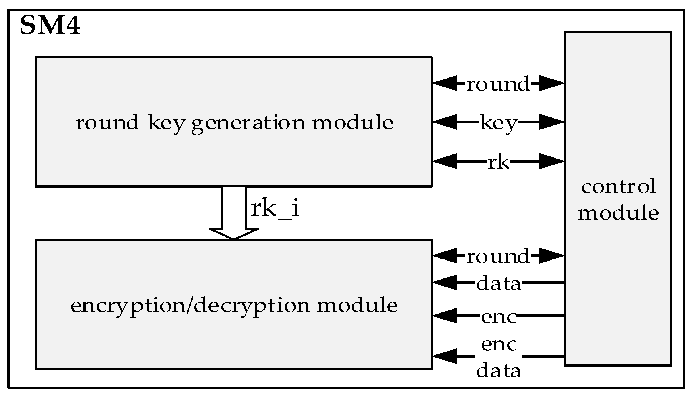
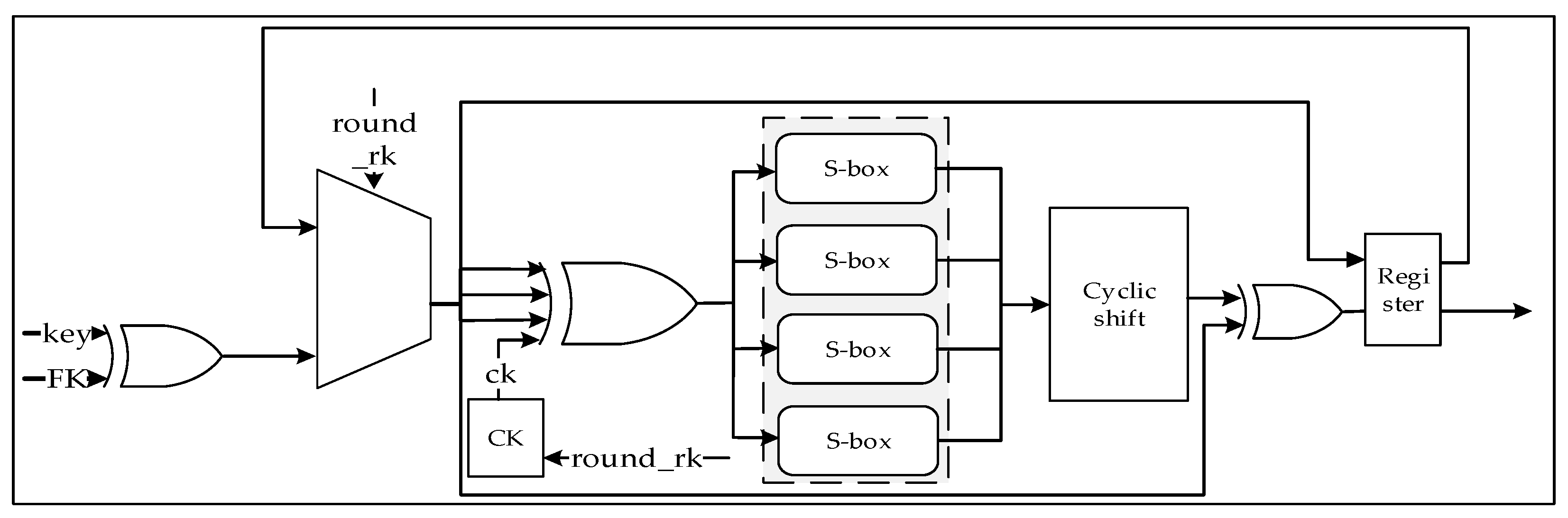
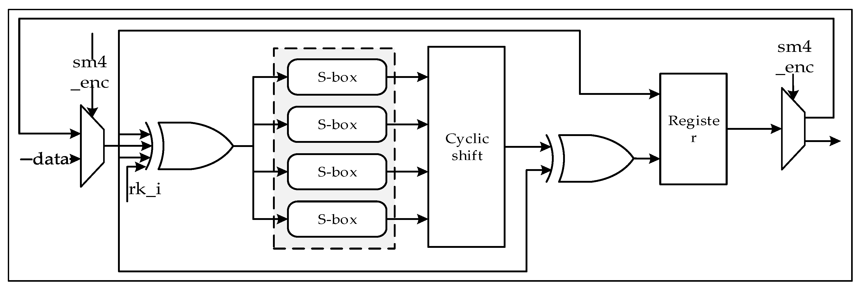
3.2. SM4 Algorithm Accelerator

We employ a cyclic hardware architecture for the SM4 algorithm accelerator, which facilitates the parallel computation of the round key-generation module and the encryption/decryption module. Figure 6 depicts the overall architecture of the SM4 algorithm accelerator. It consists of three parts, including the control module, the round key-generation module, and the encryption/decryption module. The control module orchestrates the parallel execution of the round key-generation module and the encryption/decryption module. The round key-generation module can dynamically update the round key in response to the key changes. Furthermore, both the round key-generation module and the encryption/decryption module have constant time cycles for encrypting the whole data block, which improves the resistance to side-channel attacks.
The round key-generation module mainly consists of an S-box module, a CK parameter module, a multiplexer, an XOR circuit, etc. The circuit architecture is shown in Figure 7, where the S-box uses combinational logic, which can reduce the number of storage units in the circuit, thereby simplifying the circuit and reducing resource consumption. Under the control of the control module, the round key-generation module completes one iteration operation per clock cycle, generates the round key r k i , and passes it to the encryption module for the next encryption calculation.
The encryption/decryption module is similar to the round key-generation module, and consists mainly of an S-box module, a multiplexer, an XOR circuit, etc. The architecture is shown in Figure 8, where the S-box uses combinational logic to implement. Under the output signal r of the round key-generation module and the control signal round encryption of the control module, the encryption module completes one substitution operation per clock cycle and outputs the cipher-text after 32 rounds of substitution operations.

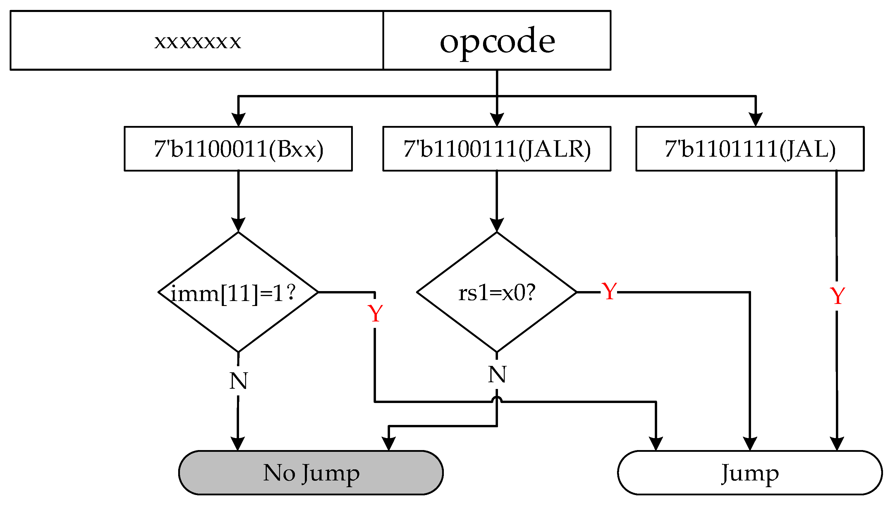
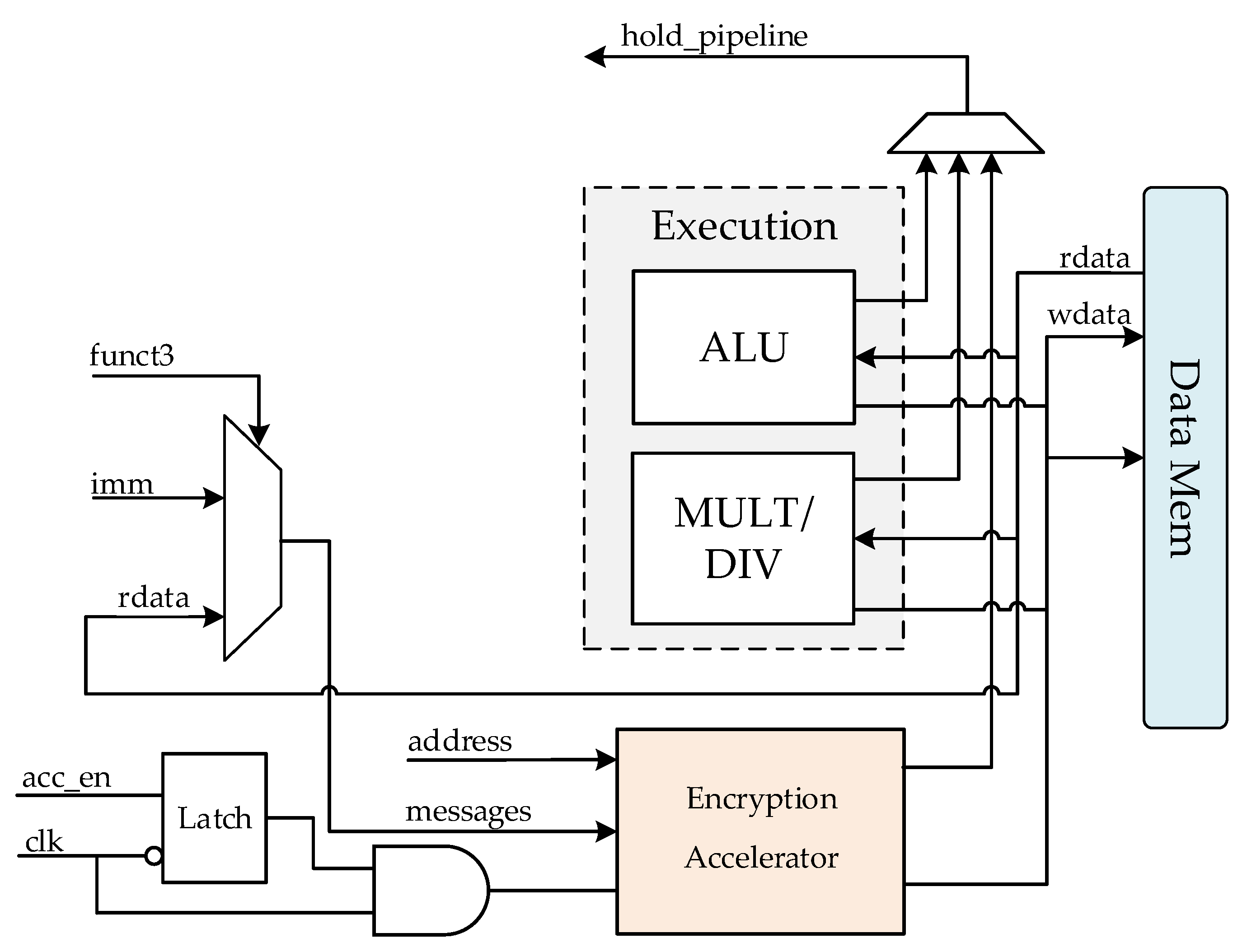
3.3. RISC-V Processor with Encryption Accelerator

The structure of the proposed RISC-V IoT processor is depicted in Figure 9, which features a two-stage pipeline architecture and supports 55 general-purpose instructions in RV32IM. It takes two clock cycles for the processor to complete the processing of one instruction. In the first clock cycle, the fetch module fetches the instruction from the instruction memory, decodes the instruction, and reads the source operands from the General Purpose Registers (GPRs) based on the result of the decoding. In the second clock cycle, the execution module performs logic or arithmetic operations on the operands based on the output from the decoding module, and then writes the results back to the GPRs or data memory. The registers without a reset are used for the data path, and the latches are used for the GPRs and the Control and Status Register (CSR) to minimize the processor’s area and power consumption.
The RISC-V architecture encompasses fundamental branch-and-jump instructions, including unconditional direct jumps (JAL), unconditional indirect jumps (JALR), and direct conditional jumps (Bxx such as BEQ, BNE) [31]. To optimize processor performance while conserving hardware resources, this study integrates static prediction techniques, as depicted in Figure 10. These techniques augment processor performance without incurring significant hardware overhead. For unconditional direct jump instruction, its target jump address can be directly calculated from the immediate data in the instruction code. For a direct jump with the condition Bxx instruction, a static prediction is used, and the jump address can be obtained directly by adding the value of the PC register and the immediate data. For unconditional indirect jump instruction, the base address used to calculate the jump target needs to be read from GPRs. It might probably cause a RAW conflict with the execution module, so if rs1 is the register ×0, the value of PC value is generated directly, and if not, in order to prevent RAW conflicts, the instruction fetch will be suspended, and the jump occurs after the execution module completes all the operations.
The hybrid encryption accelerator is invoked through five custom instructions that use the reserved opcodes’ space of RISC-V ISA, including SM3 algorithm encryption, SM4 algorithm encryption, and SM4 algorithm decryption. Figure 11 lists all the custom instructions. The extended instruction “sm3sw” performs single-word SM3 algorithm encryption, “sm3mw” performs multi-word SM3 algorithm encryption, and “sm3iw” performs immediate-number SM3 algorithm encryption. The extended instruction “sm4dec” performs SM4 algorithm decryption, and the “sm4enc” algorithm performs SM4 encryption. According to the RISC-V instruction specification, the 7-bit binary number 0001011 is selected to be the opcode of the extension instruction in order to distinguish it from other types of instructions. To distinguish the function of the extension instructions, “funct3” is utilized.
As shown in Figure 12, the encryption accelerator is integrated into the execution stage of the RISC-V processor. When a custom instruction is executed, the message to be encrypted is fetched from the data memory and sent to the encryption accelerator. The encryption accelerator initiates the corresponding cryptographic procedures based on the instruction opcode. During the encryption process, the encryption accelerator emits a pause signal to the control module to stall the processor’s pipeline. When the encryption operation is finished, the final hash value is automatically written back to the memory block. Then, the processor’s pipeline is resumed and the next instruction is fetched. To reduce the processor power consumption, a clock-gating mechanism is employed to turn off the clock signal of the encryption accelerator when it is idle.
The proposed hybrid encryption system combines the advantages of SM3 and SM4 algorithms and achieves a balance among encryption security, high speed, and key-management convenience. The basic principle is that, to fulfill the demand of high-rate encryption/decryption transmission, the system uses the SM4 algorithm to quickly encrypt/decrypt massive application data and uses the SM3 hash algorithm to compare the hash values of the plaintext before and after encryption/decryption, which prevents the information from being tampered during transmission. Because of the hybrid use of two different encryption algorithms, the proposed hybrid encryption system can realize high-speed encryption/decryption and verification operations for large numbers of data. The encryption/decryption process is summarized in Figure 13.
Assuming that the data to be encrypted and transmitted are the plaintext message m , the specific encryption/decryption transmission process is as follows: the sender uses the SM4 algorithm to encrypt the plaintext message and generate the SM4 ciphertext, and uses the SM3 algorithm to calculate the hash value of the plaintext message. After the calculation is completed, the two sets of data are packaged and sent to the receiver through the transmission channel. After receiving the data, the receiver first splits the data and obtains the SM4 ciphertext, then uses the SM4 algorithm to decrypt the SM4 ciphertext and obtains the unverified parameter plaintext; then, the receiver uses the SM3 algorithm to calculate the hash value of the parameter plaintext and compares it with the received hash value. If they are consistent, it means that the data have not been tampered with during transmission, and the plaintext message can be output, completing the decryption; if the two sets of data digests are inconsistent, it means that the data have been tampered with during transmission, and the decrypted data have security risks. The system issues a warning and exits decryption.

4. Results

4.1. Performance Analysis

The encryption algorithm necessitates repetitive arithmetic computations, involving a multitude of fundamental algorithmic instructions. By employing custom instructions in Figure 11, we achieve a significant reduction in both the number of instructions and clock cycles required for these arithmetic processes, consequently yielding a noteworthy enhancement in the algorithm’s throughput rate. We quantitatively assess the efficiency of these custom instructions by measuring and comparing encryption time and throughput rates between the hardware acceleration and traditional software schemes. Table 1 and Table 2 list several test values of the encryption time and throughput rate for different message lengths. Both schemes operate at a fixed-system clock frequency of 50 MHz. It is obvious from the result that the custom instructions show great efficiency. For different message lengths, the improvement ratio of the SM3 algorithm will be 131.24–318.62, and that of the SM4 algorithm will be 33.56–59.18.
In this section, we evaluate our implementations against previous work in terms of frequency, number of gates, throughput, and throughput frequency ratio (TFR). Table 3 and Table 4 present a performance comparison between our SM3 and SM4 algorithm accelerator and various stand-alone hardware SM3 and SM4 algorithm accelerators documented in the literature.
Compared to the SM3 standard architecture implementations described in [32], our work has achieved a noteworthy 26.4% reduction in the number of logic gates. Additionally, we have achieved a significant 2.7× increase in the throughput frequency ratio, enhancing the overall performance of the system. In [33], a design methodology is proposed for a novel dual-path parallel adder known as the Two Parallel Road Adder. This design methodology incorporates the utilization of the CSA structure, resulting in a substantial reduction in clock delay along the critical path compared to prior research efforts. Reference [34] employed task scheduling and hardware resource optimization techniques in the design of expansion modules, as well as task scheduling and critical path optimization techniques in the compression module design. This innovative architecture reduces the number of registers by approximately 3.11× and achieves a throughput of 263 Mbps under a 36 MHz clock. Compared to [33,34], our implementations have at least 3.25× and 2.8× increase in the throughput frequency ratio, respectively. Compared to [35], we achieved a higher throughput frequency ratio with approximately the same area. The proposed SM3 architecture in [36] achieves optimization at both the algorithm and circuit levels. The circuit design effectively overcomes the limitations of the conventional algorithm flow by eliminating the “blocking point” on the critical path and introducing four parallel compensation operations to restructure the algebraic framework. However, the complexity of the circuit in [36] remains a challenge. In comparison to [36], our circuit reduces the number of logic gates by 39%.
In [37], the 4-stage-pipelined SM4 cipher circuit is implemented with 18,609 gates, delivering a remarkable throughput of 2Gbps. Additionally, the unpipelined SM4 circuit with 11,535 gates achieves a throughput rate of 570 Mbps. We achieve a significant reduction of 37.4% and 61.18% in the number of logic gates compared with the unpipelined scheme and the 4-stage-pipelined scheme in [37], respectively. Reference [38] designs a compact SM4 algorithm circuit based on reusing the S-box in key schedule and round transformation, achieving a throughput of 272.7 [email protected] MHz. In comparison to [38], our circuit exhibits a throughput frequency ratio that is 1× higher. Compared to [39], our circuit has achieved a reduction in the number of logic gates by 14.89%. When compared to [40], we achieved lower gate amount with approximately the same throughput frequency ratio.

4.2. FPGA Implementation

We employed the Xilinx A7-100T FPGA experimental platform with a clock frequency set at 50 MHz. Table 5 provides an overview of the LUT (lookup table) and FF (flip-flop) resource utilization for the proposed processor, both with and without the hybrid encryption accelerator. In order to facilitate comparisons, we also present the relevant parameters for two other open-source RISC-V IoT processors, namely, the Hummingbird E203 [41] and XuanTie E902 [42], utilizing similar experimental platforms. The Hummingbird E203 processor is a 32-bit RISC-V architecture IP developed by Nuclei Systems Technology for low-power, small-area scenarios. The XuanTie E902 is an extremely low-power, low-cost embedded CPU core, which provides the operating efficiency and performance of a 32-bit embedded CPU at the cost of an 8-bit CPU. And the XuanTieE902 has been widely used in AI accelerators, industry control MCU, and wireless MCU. It is important to note that neither of these two open-source processors integrates the hybrid encryption accelerator. From the data in the Table 5, it is evident that the resource utilization of our proposed design without the accelerator is diminished by 57.3% when compared to the Hummingbird E203. Furthermore, with the inclusion of the accelerator, the resource utilization of our proposed design experiences a reduction of 39.1%. In comparison to the XuanTie E902, the resource utilization of our proposed design without the accelerator showcases a substantial decrease of 76.3%. With the accelerator, the resource utilization of our proposed design is reduced by 66.2%. This improvement can be attributed to the optimized pipeline architecture and efficient utilization of lookup tables and flip-flops in our design. Compared to the two-level variable-length pipeline of the Hummingbird E203, the pipeline architecture designed in this paper is more concise, simplifying data processing and reducing resource requirements. In comparison to the XuanTie E902, this paper extensively employs module reuse in the design, minimizing the utilization of lookup tables and flip-flops to the maximum extent.

4.3. ASIC Implementation

To further validate the proposed processor design architecture, we use Synopsys’ Design Compiler to synthesize the processor alongside two other open-source processors using the 90 nm CMOS process, and the synthesis results are given in Table 6. The back-end place and route procedure was carried out using Synopsys’ Integrated Circuit Compiler, with the final layout of the proposed processor core displayed in Figure 14. Table 6 enumerates several pivotal parameters, encompassing CoreMark performance, logic gate count, and chip area. In comparison to the Hummingbird E203, our processor attains a 10% reduction in power consumption coupled with a 32.5% decrease in circuit area. Similarly, when compared to the XuanTie E902, our processor showcases a 34.8% reduction in power consumption and a 57.1% contraction in circuit area.

5. Conclusions

This paper introduces a low-power RISC-V processor enriched with an integrated hardware hybrid algorithm accelerator, catering to IoT applications. The hardware accelerator yields substantial throughput enhancements in contrast to conventional software-based approaches. The processor core was meticulously designed and subsequently assessed on both an FPGA platform and 90 nm CMOS technology. The outcomes affirm that the proposed processor core exhibits diminished resource consumption in terms of area and power when compared to two open-source RISC-V IoT processors. This design achieves an effective equilibrium between performance and resource utilization, rendering it well-suited for IoT applications. Future work includes support for multiple encryption algorithms and further optimization for lower power consumption and higher throughput.

Author Contributions

Conceptualization, W.Z. and S.Y.; methodology, W.Z. and S.Y.; software, S.Y.; validation, W.Z., S.Y., L.S. and J.H.; formal analysis, S.Y.; investigation, L.S. and J.H.; resources, S.Y.; data curation, S.Y. and L.S.; writing—original draft preparation, S.Y.; writing—review and editing, W.Z. and S.Y.; visualization, J.H; supervision, W.Z.; project administration, W.Z.; funding acquisition, W.Z. All authors have read and agreed to the published version of the manuscript.

Funding

This research was funded by the science and technology innovation program of Hunan Province (2023GK2036) and by the Postgraduate Scientific Research Innovation Project of Hunan Province (CX20220962).

Data Availability Statement

The data presented in this study are available on request from the corresponding author.

Conflicts of Interest

The authors declare no conflict of interest.

Abbreviations

The following abbreviations are used in this manuscript:
IoTInternet of Things
RISC-VReduced Instruction Set Computing—Five
ISAInstruction Set Architecture
AESAdvanced Encryption Standard
RSARivest–Shamir–Adleman
MD5Message Digest Algorithm 5
SHA-2Secure Hash Algorithm 2
FPGAField-Programmable Gate Array
CMOSComplementary Metal–Oxide–Semiconductor
ECCElliptic Curve Cryptography
CPU Central Processing Unit
ALUArithmetic Logical Unit
SHA-256Secure Hash Algorithm 256-bit
ASICApplication-Specific Integrated Circuit
FSMFinite State Machine
RAWRead After Write
LUTLook Up Table

References

  1. Bertino, E. Data Security and Privacy in the IoT. In Proceedings of the 19th International Conference on Extending Database Technology (EDBT), Bordeaux, France, 15–18 March 2016; pp. 1–3. [Google Scholar]
  2. Patil, P.; Sangeetha, M.; Bhaskar, V. Blockchain for IoT access control, security and privacy: A review. Wirel. Pers. Commun. 2021, 117, 1815–1834. [Google Scholar] [CrossRef]
  3. Bhanot, R.; Hans, R.; Applications, I. A review and comparative analysis of various encryption algorithms. Int. J. Secur. Its Appl. 2015, 9, 289–306. [Google Scholar] [CrossRef]
  4. Daemen, J.; Rijmen, V. AES Proposal: Rijndael; Free University of Brussels: Ixelles, Belgium, 1998. [Google Scholar]
  5. Huan, L.; Lei, Z.; Wenling, W.U. Fast software implementation of SM4. J. Univ. Chin. Acad. Sci. 2018, 35, 180. [Google Scholar]
  6. Milanov, E.J.R.L. The RSA Algorithm; Massachusetts Institute of Technology: Cambridge, MA, USA, 2009; pp. 1–11. [Google Scholar]
  7. Zhang, Y.; He, D.; Zhang, M.; Choo, K.-K.R. A provable-secure and practical two-party distributed signing protocol for SM2 signature algorithm. Front. Comput. Sci. 2020, 14, 143803. [Google Scholar] [CrossRef]
  8. Rivest, R. The MD5 Message-Digest Algorithm; Massachusetts Institute of Technology: Cambridge, MA, USA, 1992; pp. 1721–2070. [Google Scholar]
  9. Chaves, R.; Kuzmanov, G.; Sousa, L.; Vassiliadis, S. Improving SHA-2 hardware implementations. In Proceedings of the Cryptographic Hardware and Embedded Systems-CHES 2006: 8th International Workshop, Yokohama, Japan, 10–13 October 2006; pp. 298–310. [Google Scholar]
  10. Yu, L.; Wang, Z.; Wang, W. The application of hybrid encryption algorithm in software security. In Proceedings of the 2012 Fourth International Conference on Computational Intelligence and Communication Networks, Mathura, India, 3–5 November 2012; pp. 762–765. [Google Scholar]
  11. Shende, V.; Kulkarni, M. FPGA based hardware implementation of hybrid cryptographic algorithm for encryption and decryption. In Proceedings of the 2017 International Conference on Electrical, Electronics, Communication, Computer, and Optimization Techniques (ICEECCOT), Mysuru, India, 15–16 November 2017; pp. 416–419. [Google Scholar]
  12. Chandu, Y.; Kumar, K.R.; Prabhukhanolkar, N.V.; Anish, A.; Rawal, S. Design and implementation of hybrid encryption for security of IOT data. In Proceedings of the 2017 International Conference on Smart Technologies for Smart Nation (SmartTechCon), Bengaluru, India, 17–19 August 2017; pp. 1228–1231. [Google Scholar]
  13. Hui, Y.; Zesong, L. Research on real-time analysis and hybrid encryption of big data. In Proceedings of the 2019 2nd International Conference on Artificial Intelligence and Big Data (ICAIBD), Chengdu, China, 25–28 May 2019; pp. 52–55. [Google Scholar]
  14. Zheng, X.; Xu, C.; Hu, X.; Zhang, Y.; Xiong, X. Systems. The software/hardware co-design and implementation of sm2/3/4 encryption/decryption and digital signature system. IEEE Trans. Comput. Aided Des. Integr. Circuits Syst. 2019, 39, 2055–2066. [Google Scholar] [CrossRef]
  15. Li, J.; Luo, Y.; Wang, F.; Gao, W.J.E. Design and Implementation of Real-Time Image Acquisition Chip Based on Triple-Hybrid Encryption System. Electronics 2022, 11, 2925. [Google Scholar] [CrossRef]
  16. Hu, Y.; Wu, L.; Wang, A.; Wang, B. Hardware design and implementation of SM3 hash algorithm for financial IC card. In Proceedings of the 2014 Tenth International Conference on Computational Intelligence and Security, Kunming, China, 15–16 November 2014; pp. 514–518. [Google Scholar]
  17. Mengdi, Z.; Xiaojuan, Z.; Yayun, Z.; Siwei, M. Overview of Randomness Test on Cryptographic Algorithms. J. Phys. Conf. Ser. 2021, 012009. [Google Scholar] [CrossRef]
  18. Cheng, Y. Study on the Encryption and Decryption of a Hybrid Domestic Cryptographic Algorithm in Secure Transmission of Data Communication. Int. J. Netw. Secur. 2022, 24, 947–952. [Google Scholar]
  19. Liu, Y.; Zhao, R.; Han, L.; Xie, J. Research and implementation of parallel optimization of SM3 algorithm based on multithread. In Proceedings of the 2022 7th International Conference on Intelligent Computing and Signal Processing (ICSP), Xi’an, China, 15–17 April 2022; pp. 330–336. [Google Scholar]
  20. Zhou, M.; Ruan, S.; Liu, J.; Chen, X.; Yang, M.; Wang, Q. vTPM-SM: An Application Scheme of SM2/SM3/SM4 Algorithms Based on Trusted Computing in Cloud Environment. In Proceedings of the 2022 IEEE 15th International Conference on Cloud Computing (CLOUD), Barcelona, Spain, 10–16 July 2022; pp. 351–356. [Google Scholar]
  21. Jiang, Z.; Yan, W.; Ding, W.; Yue, L.; Ding, Q. SM4 Chaotic Masking Scheme against Power Analysis Based on FPGA. Int. J. Bifurc. Chaos 2022, 32, 2250110. [Google Scholar] [CrossRef]
  22. Rao, J.; Cui, Z.J.A.S. Chosen Plaintext Combined Attack against SM4 Algorithm. Appl. Sci. 2022, 12, 9349. [Google Scholar] [CrossRef]
  23. Wang, Z.; Dong, H.; Chi, Y.; Zhang, J.; Yang, T.; Liu, Q. Research and Implementation of Hybrid Encryption System Based on SM2 and SM4 Algorithm. In Proceedings of the 9th International Conference on Computer Engineering and Networks, Dalian, China, 22–24 October 2021; pp. 695–702. [Google Scholar]
  24. Waterman, A.S. Design of the RISC-V Instruction Set Architecture; University of California: Berkeley, CA, USA, 2016. [Google Scholar]
  25. Waterman, A.; Lee, Y.; Avizienis, R.; Patterson, D.A.; Asanovic, K. The RISC-V instruction set manual volume II: Privileged architecture version 1.7. Tech. Rep. 2015, 1–91. [Google Scholar]
  26. Flamand, E.; Rossi, D.; Conti, F.; Loi, I.; Pullini, A.; Rotenberg, F.; Benini, L. GAP-8: A RISC-V SoC for AI at the Edge of the IoT. In Proceedings of the 2018 IEEE 29th International Conference on Application-specific Systems, Architectures and Processors (ASAP), Milano, Italy, 10–12 July 2018; pp. 1–4. [Google Scholar]
  27. Patterson, D. 50 Years of computer architecture: From the mainframe CPU to the domain-specific tpu and the open RISC-V instruction set. In Proceedings of the 2018 IEEE International Solid-State Circuits Conference-(ISSCC), San Francisco, CA, USA, 11–15 February 2018; pp. 27–31. [Google Scholar]
  28. Patterson, D.; Waterman, A. The RISC-V Reader: An Open Architecture Atlas; Strawberry Canyon: Elsevie, CA, USA, 2017. [Google Scholar]
  29. De, D.; Das, J.C. Design of novel carry save adder using quantum dot-cellular automata. J. Comput. Sci. 2017, 22, 54–68. [Google Scholar] [CrossRef]
  30. Bahadori, M.; Kamal, M.; Afzali-Kusha, A.; Afsharnezhad, Y.; Salehi, E.Z.J.I. CL-CPA: A hybrid carry-lookahead/carry-propagate adder for low-power or high-performance operation mode. Integration 2017, 57, 62–68. [Google Scholar] [CrossRef]
  31. Bowhill, W.J.; Allmon, R.L.; Bell, S.L.; Cooper, E.M.; Donchin, D.; Edmondson, J.; Fischer, T.; Gronowski, P.; Jain, A.; Kroesen, P. A 300 MHz 64 b quad-issue CMOS RISC microprocessor. In Proceedings of the ISSCC’95-International Solid-State Circuits Conference, San Francisco, CA, USA, 5–17 February 1995; pp. 182–183. [Google Scholar]
  32. Ao, T.; He, Z.; Rao, J.; Dai, K.; Zou, X. A compact hardware implementation of SM3 hash function. In Proceedings of the 2014 IEEE 13th International Conference on Trust, Security and Privacy in Computing and Communications, Beijing, China, 24–26 September 2014; pp. 846–850. [Google Scholar]
  33. Yong-peng, Y.; Ying-jian, Y.; Wei, L.J. High speed ASIC design and implementation of SM3 algorithm. Microelectron. Comput. 2016, 33, 21–26. [Google Scholar]
  34. Zheng, X.; Hu, X.; Zhang, J.; Yang, J.; Cai, S.; Xiong, X.J.E. An efficient and low-power design of the SM3 hash algorithm for IoT. Electronics 2019, 8, 1033. [Google Scholar] [CrossRef]
  35. Ma, Y.; Xia, L.; Lin, J.; Jing, J.; Liu, Z.; Yu, X. Hardware performance optimization and evaluation of SM3 hash algorithm on FPGA. In Proceedings of the Information and Communications Security: 14th International Conference, ICICS 2012, Hong Kong, China, 29–31 October 2012; pp. 105–118. [Google Scholar]
  36. Zang, S.; Zhao, D.; Hu, Y.; Hu, X.; Gao, Y.; Du, P.; Cheng, S. A high speed SM3 algorithm implementation for security chip. In Proceedings of the 2021 IEEE 5th Advanced Information Technology, Electronic and Automation Control Conference (IAEAC), Chongqing, China, 12–14 March 2021; pp. 915–919. [Google Scholar]
  37. Niu, Y.; Jiang, A. The low power design of SM4 cipher with resistance to differential power analysis. In Proceedings of the Sixteenth International Symposium on Quality Electronic Design, Santa Clara, CA, USA, 2–4 March 2015; pp. 470–474. [Google Scholar]
  38. Bu, X.; Wu, N.; Zhou, F.; Yahya, M.R.; Ge, F. ’A Compact Implementation of SM4 Encryption and Decryption Circuit’. In Proceedings of the Lecture Notes in Engineering and Computer Science: Proceedings of The World Congress on Engineering and Computer Science, San Francisco, CA, USA, 22–24 October 2019; pp. 22–24. [Google Scholar]
  39. Chen, G.W.; Qiao, S.S.; Yong, H. Design of Low Complexity SM4 Block Cipher IP Core. Sci. Technol. Eng. 2013. [Google Scholar]
  40. Fu, H.; Bai, G.; Wu, X. Low-cost hardware implementation of SM4 based on composite field. In Proceedings of the 2016 IEEE Information Technology, Networking, Electronic and Automation Control Conference, Chongqing, China, 20–22 May 2016; pp. 260–264. [Google Scholar]
  41. Zhenbo, H. Teach You to Design CPUs Hand-in-Hand; RISC-V Processor, People’s Posts and Telecommunications Press: Beijing, China, 2018. [Google Scholar]
  42. Chen, Y.; Chen, H.; Chen, S.; Han, C.; Ye, W.; Liu, Y.; Zhou, H.J.S. DITES: A Lightweight and Flexible Dual-Core Isolated Trusted Execution SoC Based on RISC-V. Sensors 2022, 22, 5981. [Google Scholar] [CrossRef] [PubMed]
Figure 1. Overall architecture of SM3 algorithm accelerator.
Electronics 12 04222 g001
Figure 2. FSM state transition diagram.
Electronics 12 04222 g002
Figure 3. Logic schematic of the expansion module.
Electronics 12 04222 g003
Figure 4. Logic schematic of the compression module.
Electronics 12 04222 g004
Figure 5. Illustration of the critical path optimization.
Electronics 12 04222 g005
Figure 6. Overall architecture of SM4 algorithm accelerator.
Electronics 12 04222 g006
Figure 7. Overall architecture of round key-generation module.
Electronics 12 04222 g007
Figure 8. Overall architecture of encryption/decryption module.
Electronics 12 04222 g008
Figure 9. Architectural block diagram of the processor core.
Electronics 12 04222 g009
Figure 10. Diagram of static branch prediction.
Electronics 12 04222 g010
Figure 11. Field definitions of the custom instruction.
Electronics 12 04222 g011
Figure 12. Encryption accelerator embedded into the processor core.
Electronics 12 04222 g012
Figure 13. Encryption and decryption process of the hybrid system.
Electronics 12 04222 g013
Figure 14. Layout of the processor.
Electronics 12 04222 g014
Table 1. Comparison of SM3 encryption delay with/without custom instructions.
Plaintext Message (Byte)Traditional Software SchemesHardware AcceleratorImprovement
Ratio
Encryption
Time (us)
Throughput Rate (MB/s)Encryption
Time (us)
Throughput Rate (MB/s)
321350.241.0231.37131.24
642380.271.4843.24159.73
1284470.291.9465.98229.35
2567600.342.8689.51264.69
51213850.374.7108.94293.66
102425310.408.38122.20301.01
204850310.4115.74130.11318.62
Table 2. Comparison of SM4 encryption delay with/without custom instructions.
Plaintext Message (Byte)Traditional Software SchemesHardware AcceleratorImprovement Ratio
Encryption Time (us)Throughput Rate (MB/s)Encryption Time (us)Throughput Rate (MB/s)
1642.760.390.6623.0859.18
256376.960.6810.2623.8235.03
10241461.310.7040.9823.8334.04
20482888.320.7181.9423.8333.56
819211,519.150.71327.723.8333.56
16,38422,960.420.71655.3823.8333.56
Table 3. SM3 algorithm accelerator performance comparison.
This Work[32]
Standard
[33][34][35][36]
Platforms (nm)901306513013040
Frequency (MHz)50200526.336216415
Gates (Gate)953712,95653706036945815,750
Throughput (Mb/s)10401506336826316196400
Throughput/Frequency20.87.536.47.37.515.4
Table 4. SM4 algorithm accelerator performance comparison.
This Work[37]
Unpipelined
[37]
Pipelined
[38][39][40]
Platforms (nm)90180180180180130
Frequency (MHz)50100100144.910050
Gates (Gate)722411,53518,609574084887612
Throughput (Mb/s)190.645702000272.7100193.9
Throughput/Frequency3.85.7201.91.03.9
Table 5. Comparison based on FPGA platforms.
DesignPlatformLUTsFFsDSP/BRAM
This work with acceleratorxc7a100t931243904/0
This work without acceleratorxc7a100t666329494/0
[41]zynq-700011,26211,2370/0
[42]xc7a100t27,14613,4340/64
Table 6. Comparison based on the 90 nm CMOS process.
This Work[41][42]
CoreMark (CoreMark/MHz)2.362.142.69
Platforms (nm)909090
Voltages (V)111
Frequency (MHz)501650
Gates (K)40.361.8114
Area (mm2)0.270.40.63
Power (mW/MHz)0.02880.0320.0442
Disclaimer/Publisher’s Note: The statements, opinions and data contained in all publications are solely those of the individual author(s) and contributor(s) and not of MDPI and/or the editor(s). MDPI and/or the editor(s) disclaim responsibility for any injury to people or property resulting from any ideas, methods, instructions or products referred to in the content.

