Article

FPGA-Based Pulse Compressor for Ultra Low Latency Visible Light Communications

Information Engineering Department, University of Florence, Via S. Marta No. 3, 50139 Firenze, Italy
*
Author to whom correspondence should be addressed.
Electronics 2023, 12(2), 364; https://doi.org/10.3390/electronics12020364
Submission received: 23 December 2022 / Revised: 5 January 2023 / Accepted: 9 January 2023 / Published: 10 January 2023
(This article belongs to the Special Issue New Technologies in Visible Light Communications)

Abstract

:
Visible Light Communication (VLC) represents an emerging technology where a short-range data connection is obtained by modulating the energy radiated by Light Emitting Diodes (LEDs) at frequencies from a few kHz up to hundreds of MHz. The bandwidth/distance performance of such links is a compromise related to the available Signal-to-Noise ratio (SNR). At present, VLC links with bandwidth beyond the Gb/s and distance limited to a few cm or distances up to 100 m but data rates of a few kb/s have been demonstrated. Chirp coding with pulse compression is a well-known technique capable of recovering useful data from low SNR signals, widely employed, for example, in radar. In spite of the possible advantages, its application in VLC has never been investigated. Unfortunately, the pulse compressor is quite calculation-intensive, and only devices like Field-Programmable-Gate-Arrays (FPGAs) can support a low-latency real-time implementation. In this paper we demonstrate a real-time VLC link based on chirp coding and pulse compression coded in FPGA. For example, a chirp with bandwidth and length of 1.7 MHz and 17.92 µs, respectively, is demonstrated to support a link at 1.56 Mb/s over 2.8 m distance and a latency below 40 µs. Moreover, the communication-distance increase achievable by chirps of increasing temporal length is demonstrated and compared to the theoretical background.

1. Introduction

Visible Light Communications (VLC) represents a novel technology [1,2] where a data channel is established by means of visible light. The information is modulated over the light by quick radiation modulations that do affect the mean intensity and are undetectable by the human eye. The recent ubiquitous substitution of incandescent and fluorescent lamps with the more efficient Light Emitting Diode (LED) lamps, which are inherently compatible with VLC [3], represents another push in the direction of the adoption of this new technology.
The fields of use and the new possibilities that this technology opens are very wide. For example, VLC can sustain or substitute the Wi-Fi or Bluetooth standards in homes and offices by exploiting the same lamps that are used for the ambient lighting. This approach not only implements more efficient energy consumption (the same energy source is exploited for both lighting and communication) but also frees frequencies from the overcrowded electromagnetic spectrum and helps to relax the frequency congestion [4]. The applications that can benefit the several advantages of the VLC technology are numerous and typically divided into indoor [5] and outdoor [6]. They include, for example, biomedical data communication in air [7] or even through the skin [8], objects and people localization [9], museal [10], data networks in harsh environments [11], vehicular communications [12], and many others.
Most of the applications presented in recent literature employ the On-Off Keying (OOK) modulation [13] for coding the informative bits in the light. This is a simple approach where the light is rapidly switched on/off, and it is implemented with basic electronics. In spite of its simplicity, this approach has been shown to be capable of supporting a bandwidth of hundreds of Mb/s over a short distance [14]. However, higher rates can be attained only through more complex modulation schemes. For example, Orthogonal Frequency Division Multiplexing (OFDM) modulation, or wavelength division multiplexing (WDM), applied to a RGB LED allowed bandwidth well beyond the Gb/s [15,16]. Other experiments focus on achieving high communication distance, though with lower bandwidth: for example, a 50 m link is reported in [17] at 19.2 kb/s rate.
In general, bandwidth performance is limited by the Signal-to-Noise Ratio (SNR), which, in turn, depends on distance. An improvement on SNR can be capitalized for a higher bandwidth, a longer distance, or a better trade-off between the two of them. Chirp coding and pulse compression represents a well-known technique for transmitting and recovering the data from noisy signals. Chirp coding has been developed especially in radar and applied for improving its penetration [18], but it is now exploited in many other fields like, for example, biomedical investigations [19] or sonar [20].
At the best of our knowledge, the advantages that this method can provide to VLC applications are still to be investigated. A possible reason can be that real-time chirp coding and pulse compression is quite demanding for the calculation effort it requires. For example, a 10 µs chirp sampled at 10 Msps is compressed through a 100-tap correlator that needs 1000 M of operation per s (MOPs). Fortunately, Field Programmable Gate Arrays (FPGAs), thanks to the hundreds of Digital Signal Processors (DSPs) they are equipped with, support easily such a heavy calculation load [21]. Thus, they represent a likely choice for the implementation of real-time chirp-modulated VLC applications.
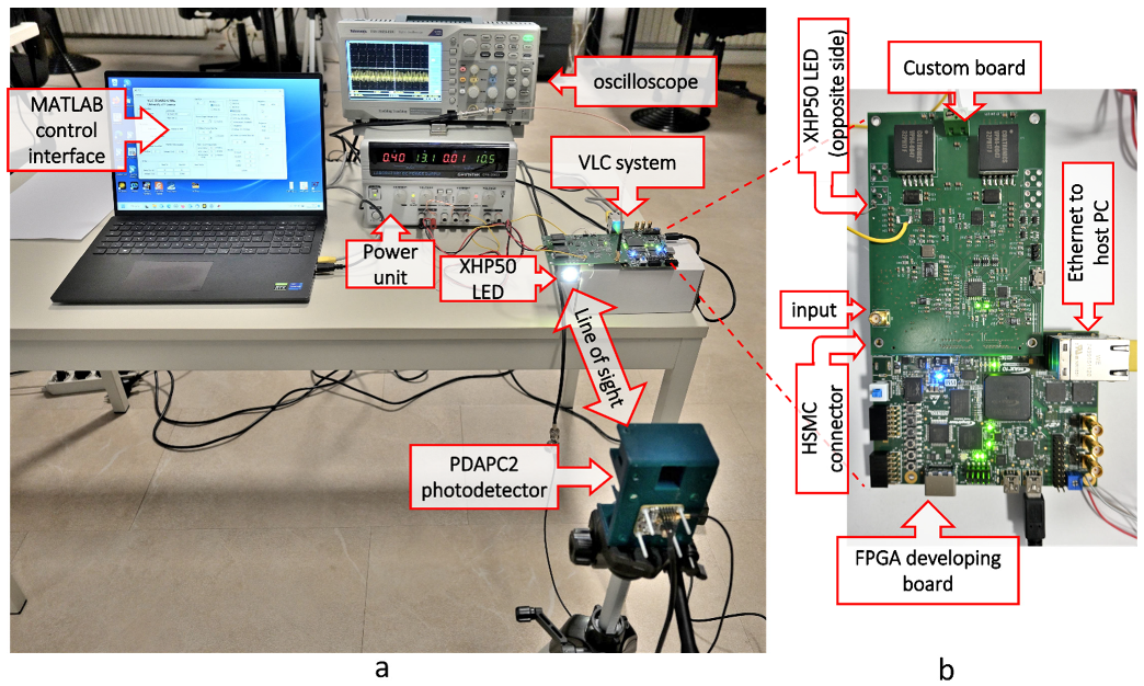
In this paper we present an ultra-low latency VLC link realized in real-time in FPGA through chirp coding in transmission (TX) and pulse compression in reception (RX). The data were subdivided in 24-bit packets, chirp-modulated in the FPGA, analog-converted, and transmitted through a phosphorous white LED (5000 K) [
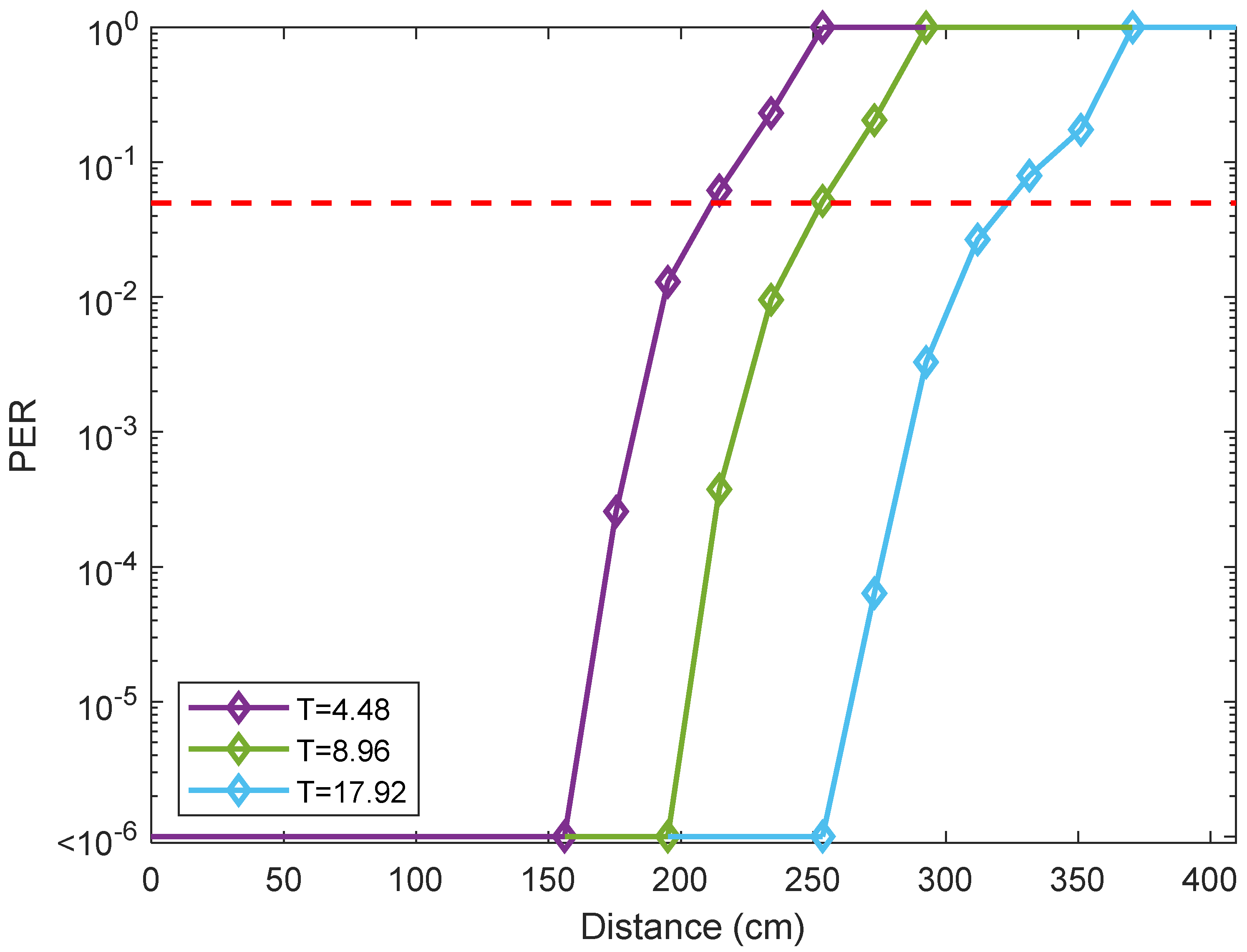
3] powered with 1 A mean current. In reception, the signal received from a photodetector was amplified, digital-converted, and, in the FPGA, compressed and reconverted in packets of bits. In the experiments, 3 different chirps (1.7 MHz bandwidth and lengths of 4.48, 8.96, 17.92 µs, respectively) are tested. The gain in communication distance attainable by chirps with higher temporal durations are measured and compared to a theoretical model. For example, a 1.56 Mb/s link over a 2.12 m distance was demonstrated by employing the 4.48 µs chirp. The communication distance raised to 3.20 m for the 17.92 µs chirp. The latency, i.e., the time needed to the data packet from the input of the transmitter to the output of the receiver, was always below 40 us.
The paper proceeds with Section 2, where the basics principles of the pulse compression are summarized; Section 3 describes the employed communication protocol; Section 4 reports about the implementations in FPGA of the chirp coder, the compressor, and the packet reconstruction; Section 5 describes the experimental set-up; Section 6 reports the measurements; finally, Section 7 discusses the results, and Section 8 closes the work.

2. Pulse Compression Basics

2.1. Theoretical Background

A very brief summary with the basic principles of the chirp pulse compression is reported below, with the intention of helping readers who are not familiar with the method. On the other hand, pulse compression is a mature technique, and more details can be easily found in books, like, for example [22,23].
The transmitted signal is typically a chirp, i.e., a signal with temporal duration T, and frequency that changes in time to span a bandwidth B = F M a x F M i n , where F M a x and F M i n are the higher and lower boundaries of the frequency interval. An important performance parameter of this method is the bandwidth-time product BT. An example of chirp where the frequency chances linearly with time is:
C H t = sin 2 π F M i n · t + B 2 T · t 2
The received signal R F R x t is processed with a filter matched to the transmitted chirp. Several techniques have been studied for the optimization of such a filter [24]; however, in the simplest case, the received signal is correlated to the chirp itself:
R t = 0 T C H τ R F R x t + τ d τ
In the positions where the R F R x t contains the transmitted chirp, the matched filter (2) produces the so-called “compressed pulse”, i.e., a pulse-shaped signal with amplitude A and width W. It can be demonstrated [22] that W ≈ 1/B and A ≈ B T . Since W < T, the pulse is “compressed”, which justifies the name of the technique. The W parameter represents the time resolution of the system, i.e., how much different chirps can be overlapped one to the other in time so that they can be individually detected in the compressed signal. Moreover, the amplitude of the compressed pulse is about A = B T with respect to the original chirp. This amplitude gain extends the pulse beyond the noise floor, represents a useful SNR gain, and, at the end, eases the data detection.
The example reported in Figure 1, generated in MATLAB (The Mathworks, Natick, MA, USA), clarifies the concept. Panel a reports a chirp with F M i n = 1 MHz and F M a x = 5 MHz, temporal duration T = 10 µs, and thus B = 4 MHz and BT product of 40. The frequency is linearly modulated by (1), like reported in Figure 1b. The spectrum of the chirp is shown in Figure 1c. Finally, after the application of the compressor filter (2), the signal assumes the peaked shape represented in Figure 1d. The width of the pulse (evaluated at −4 dB) is roughly W ≈ 1/B = 0.25 µs, and the amplitude gain is A ≈ 6.3.

2.2. Distance Gain in VLC through Pulse Compression

The SNR gain that the chirp modulation produces can be exploited to extend the communication distance or the data rate in VLC. In this work we focus in particular on the distance gain. In this paragraph, a simple model on the relation between the maximum communication distance and chirp length is obtained.
The amplitude of the radiated light is expected to decay proportionally to the square of the distance R between the LED and the receiver [25]; on the other hand, the same amplitude increases with the radix of the chirp duration T and bandwidth B (see above). Thus, for a receiver with a given input noise and sensitivity, the distance and chirp duration are approximatively related through:
K = B T R 2
where K is a constant that depends on several factors like the receiver sensitivity, the LED power, the optical gain of the link, the Bit-Error-Rate (BER), etc. For example, increasing N-fold the chirp duration and leaving all of the other parameters unaltered produces:
K = B T R 1 2 = B N T R 2 2
where R 1 and R 2 are the communication distances achieved with chirps of length T and NT, respectively. From (4) we finally have:
R 2 = N 4 · R 1

3. Communication Protocol

3.1. Trasmission Modulation

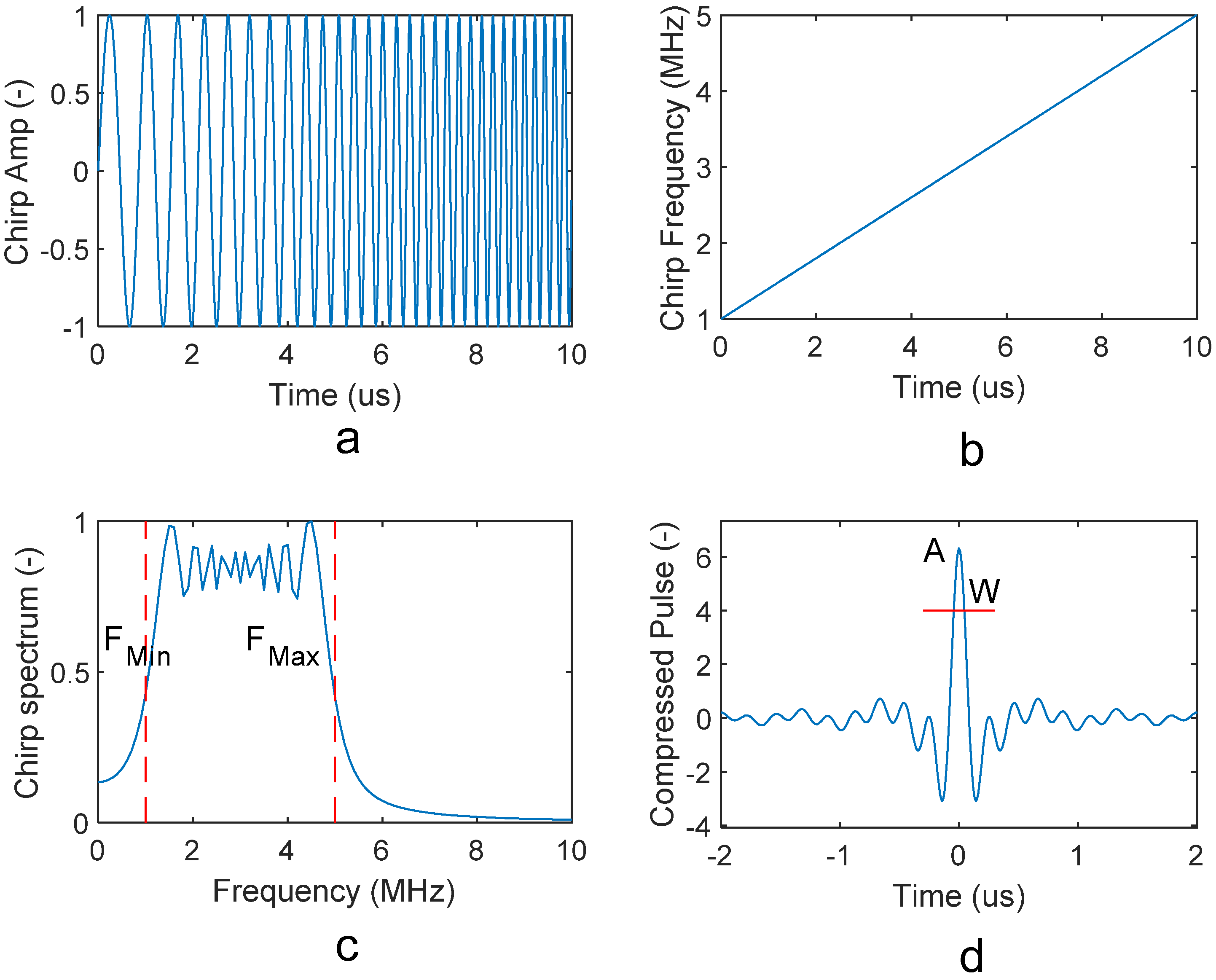
In the protocol proposed in this work, the data are represented by a continuous bitstream (0, 1 values) that feeds the modulator. The modulator applies the chirp coding as described below. Data are modulated by a linear chirp (1) selected among 3 different choices. These chirps feature the same frequency content but different temporal durations. The bandwidth B = 1.7 MHz ( F M i n = 100 kHz, F M a x = 1.8 MHz), common to the 3 of them, is selected to fit the features of the LED employed in the transmitter, like it will be clarified in Section 5.2, and grants a temporal resolution of W = 1/B = 588 ns. The durations of the chirps differ and are set to T = 4.48, 8.96 and 17.92 µs, respectively. The corresponding BT was 6.8, 13.6, 27.2.
The modulator is implemented in a digital processor, where the signals are sampled at rate T T C = 80 ns ( 1 / T T C = 12.5   M H z ). The 3 chirps are thus composed by N S = T / T T C = 56, 112, 224 samples, respectively. Table 1 summarizes the chirps features.
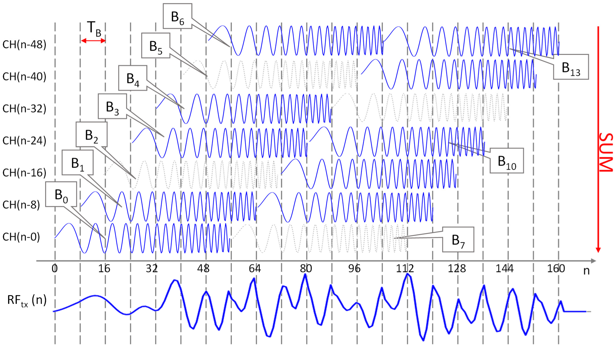
In this protocol we transmitted the chirp for every ‘1’ bit of the bitstream, whereas for ‘0′ bit the chirp was not transmitted. We transmitted a new bit every 8 T T C , i.e., every 640 ns. This time fits with the system resolution of W = 1/B = 588 ns. Since a new chirp is potentially transmitted every 8 T T C , the transmission signal is composed by the summation of more chirps overlapped with different phases. When a sequence of all ‘1’ is transmitted, the maximum number of chirps must be summed up for every time instant; this maximum is:
N C = T T B .
The maximum corresponds to N C = 7, 14, 28 for the 3 chirps of Table 1, respectively.
The transmission signal can be formally represented by:
R F t x n = i = n 8 n 8 + N C 1 B i · C H P n 8 i · T T C
Here C H P t is the periodic extension of C H t with period T ; B x is the bit at position ‘x’ in the bitstream and has value ‘0’ or ‘1’; n is the sample index; and x represents the integer part of x . Figure 2 reports an example generated in MATLAB that clarifies the modulation scheme for the chirp with T = 4.48 µ.
The horizontal axis represents index sample n; the distance among the grid vertical lines is of T B = 8 samples. In the upper part, the seven rows report as many chirp signals delayed of T B one with respect to the previous. The chirps repeat periodically every T = 7 · T B   = 56 samples. In the example, the arbitrary bitstream “11011101011011” is transmitted with LSB first, and every chirp is labelled with the associated bit (Bit 0-13 in the figure). Chirps corresponding to ‘0’ and ‘1’ bits are represented in gray and blue colors, respectively. The transmission signal R F t x (n), shown in the bottom part of the figure, is obtained by summing the seven signals at the same temporal index. Each signal is a chirp if the bit is ‘1’ or a null signal if the bit is ‘0’.
The R F t x n signal, calculated by (7), is converted to current and amplified. This is a 0-mean signal that cannot directly feed the LED. This signal is added to a constant current, that represents the mean LED luminosity. The resulting current, which is always positive, is applied to the transmission LED.

3.2. Format of the Data Packet

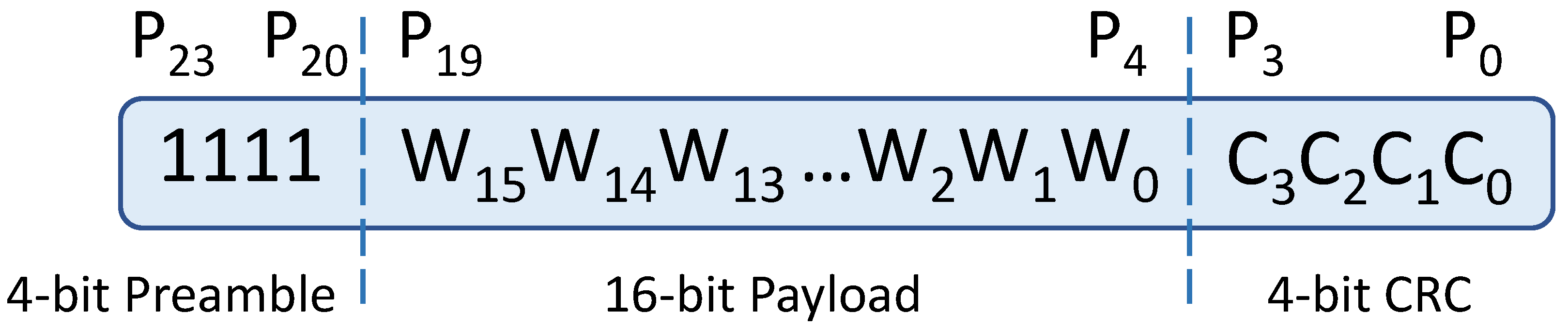
The data to be transmitted is organized in 24-bit packets with the simple format sketched in Figure 3. Data to be transmitted (the payload) is subdivided in words of 16-bit each (i.e., 2-byte). A fixed preamble of 4-bit “1111” is added before the payload. It will help the receiver to synchronize to the packets’ boundaries. Finally, a 4-bit Check Redundancy Code (CRC) is appended at the end of each packet, so that the receiver can check the data integrity. In Figure 3, the packet is represented with bits P23-0, the payload is W15-0, and the CRC has bits C3-0.
The CRC is calculated by subdividing the preamble and payload in 5 sub-words of 4-bit each, that are added. Carry to the 5th bit is discarded in the process:
C R C = i = 0 5 P 4 i + 3 P 4 i + 2 P 4 i + 1 P 4 i + 0
The 24-bit packets are queued one after the other, with no delay in between. The sequence produces a bitstream that is coded with the chirps, like described above.

3.3. Reception Decoding

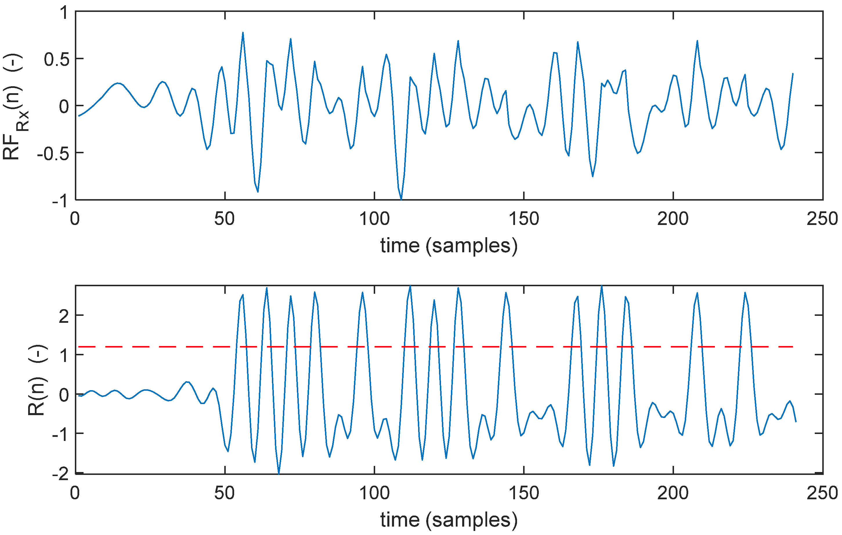
The signal received, R F r x t , is band-pass filtered, amplified, and digitally converted at rate T R C = T T C . Then, it is correlated with the original chirp signal (2) according to the pulse compression technique. The resulting compressed signal R n presents a ‘peak’ for every ‘1’ bit of the original bitstream and no peak for every ‘0’ bit. A simple amplitude threshold can be used to recover the bitstream. Figure 4 shows, for example, the received and the compressed signals for the arbitrary bit sequence “111101011101001110010100” that corresponds to the 24-bit data packet with the 16-bit payload “0101110100111001”. The bitstream is recovered with a threshold at half-amplitude.
For every new bit that is decoded, the last 24-bit are considered a prospective packet. The preamble and the CRC are checked. If the result is negative, the process repeats with the next bit. If it is positive, the payload is extracted, and the process jumps to the next 24 bits. More details are given in the FPGA implementation.

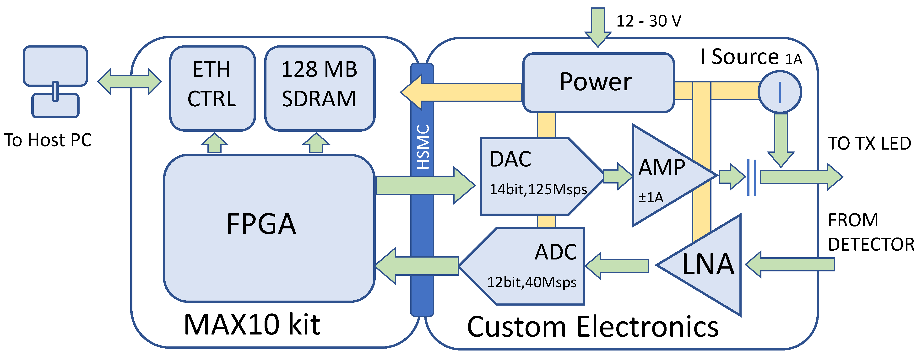
4. FPGA Implementation

The FPGA code was developed in very high-speed integrated circuits Hardware Description Language (VHDL) in Quartus Prime 20.1 (Intel Corp, Santa Clara, CA, USA). The code includes the transmitter and the receiver, detailed in the following sections.

4.1. The Transmitter

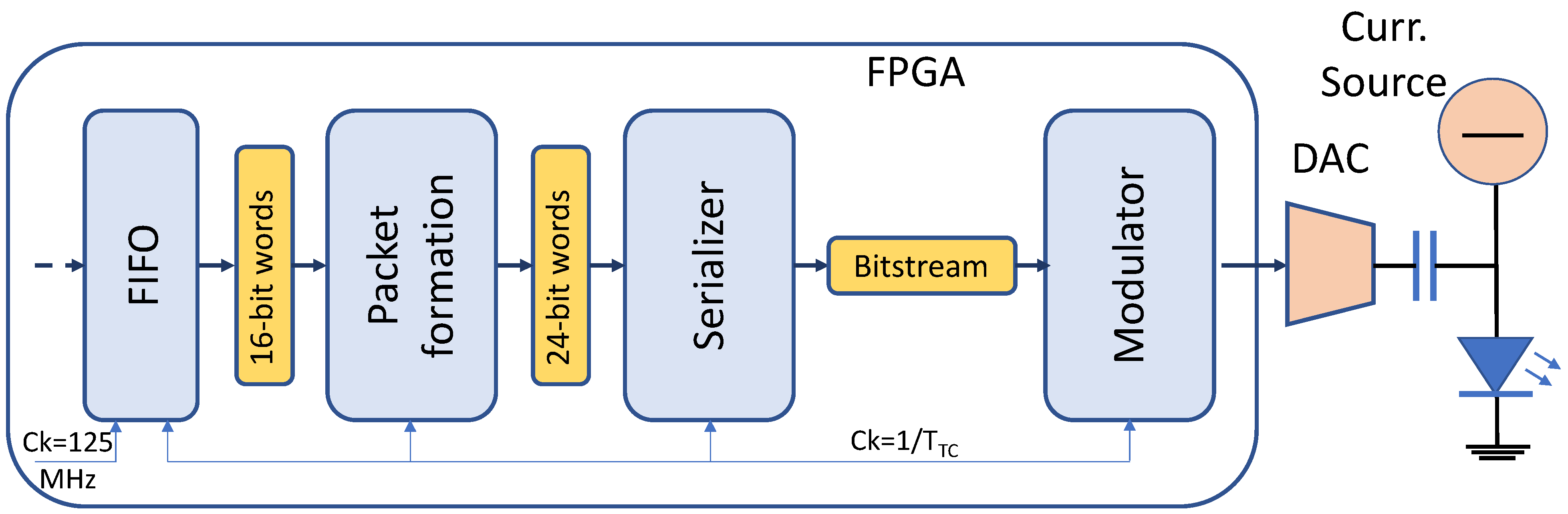
The architecture of the transmitter is sketched in Figure 5. It is composed by several processing blocks connected through an Avalon® streaming bus [26]. Data, moved by the bus, cross all the blocks serially. The data flow is regulated through the backpressure technique implemented in the Avalon® bus: each block, when it is not ready to sink data, rises a ‘busy flag’ that stalls the data flow from the previous block. On the other hand, the processing chain is designed so that each block grants the availability of data as soon as the successive block is ready to accept them. This way, the rate of the data flow along the chain is imposed by the last block, which is the “Modulator”. This architecture grants a constant and uninterrupted data flow at sample rate towards the Digital-to-Analog Converter (DAC) and the LED.
Data words to be transmitted are buffered in a First-In-First-Out (FIFO) memory. The FIFO separates the clock domains of the FPGA core that operates at 125 MHz from the transmitter domain that operates at the lower frequency of 1 / T T C . The 16-bit payload is moved from the FIFO to the next block that formats the 24-bit packet. This block calculates the CRC and builds the packet by adding the CRC and the preamble. The 16-bit input words and 24-bit output words flow at the rate of one word for every 24 bits transmitted, i.e., 24 / T B = 3 / T T C . Thus, the block has three clock cycles to process each word. This is a simple block, and no further details are here provided.
The next block is the Serializer, which sinks the 24-bit word in parallel and outputs it serially, providing the bitstream for the modulator. The output rate is 1 / T B . Similarly to the previous block, no further details are necessary for this simple step.
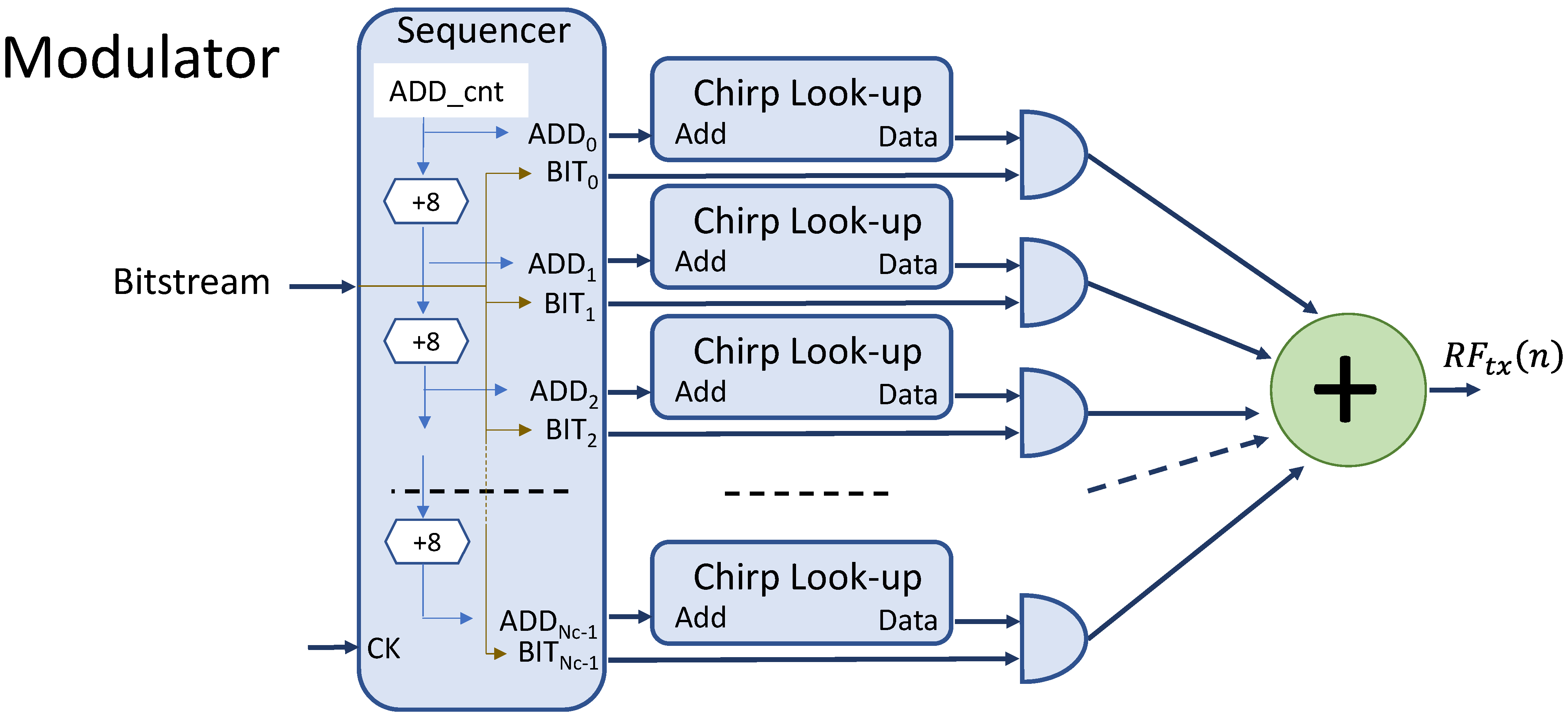
The modulator is by far the most complex part of the transmitter and deserves more attention. Its internal architecture is detailed in Figure 6.
The modulator is fed by the bitstream prepared by the previous blocks and produces in outputs the samples of the signal that, once converted in current, are transferred to the LED. It works with the clock CK at rate 1 / T T C , and thus every 8 CK cycles it accepts in input and processes a new bit. On the other hand, every CK cycle a new sample of R F t x n is produced in output.
Although the architecture of the modulator is the same, its complexity scales with the chirp length. In fact, the number, Nc, of chirps to be added for each output sample rises with the chirp length, like stated by (6). The modulator should basically add the Nc chirps, suitably phased and masked by the corresponding data bit. This task is achieved by employing Nc identical look-up tables that store: the samples of the chirp; Nc ‘AND’ gates used for zeroing the corresponding look-up output; a Nc-input adder; and a sequencer block that generates the look-up addresses, the gates masking inputs, and the circuit timing.
The sequencer generates the addresses to the chirp look-up tables through the counter ADD_cnt followed by a chain of adders. The n-th address in the chain, ADDn (0 ≤ n ≤ Nc-1), is obtained by summing the value 8·n, so that the chirp n is delayed by 8 samples with respect to the chirp n-1. The sums are modulo N S , where N S is the number of chirp samples. Every CK cycle, the ADD_cnt is incremented. When the ADDn output is pushed back to 0 (because it reached N S 1 ), the corresponding bit BITn is loaded with the next bit in the input bitstream. This bit feeds an input of the AND gate, so if the bit is zero, the chirp samples are zeroed; otherwise, the samples reach the adder unaffected. Finally, the adder performs the summation of the Nc chirps and produces the output sample. The adder is implemented in four pipelined stages to facilitate the FPGA time closure at the desired clock frequency.
The following pseudo-code clarifies how the sequencer calculates its outputs:
Init:
       ADD_cnt = 0
Loop:
       ADD_cnt = ADD_cnt + 1
       ADD0 = ADD_cnt
       ADDn = Addn-1 + 8 (1 ≤ n ≤ Nc-1)
       If ADDn = Ns (0 ≤ n ≤ Nc-1)
       ADDn = 0
       BITn = Next BIT
       End if
       Wait next CK rising edge
End Loop

4.2. The Receiver

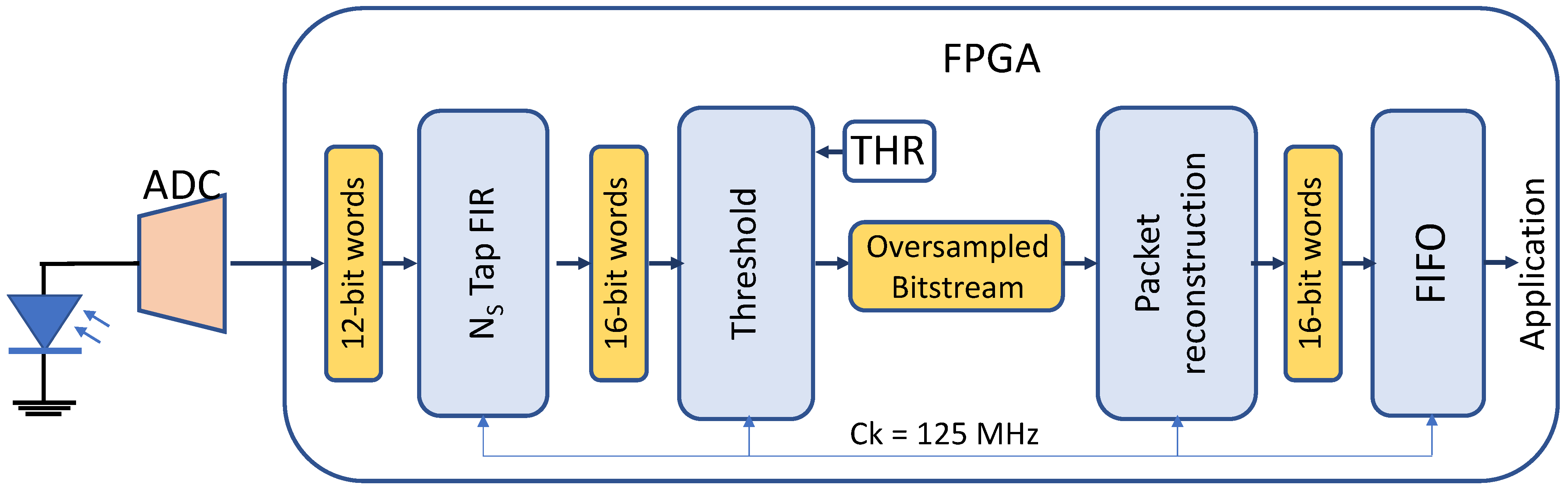
The architecture of the receiver is sketched in Figure 7.
The signal received by the photodetector is amplified and converted to digital at the rate 1 / T R C = 12.5   MHz and 12-bit resolution. The samples are then moved in the FPGA. Here, they enter the compressor filter that is realized through a Finite Impulse Response (FIR) filter at N S taps, whose coefficients W i are obtained by mirroring in time the chirp samples:
W i = C H N S i         0 i N S 1
This approach is particularly beneficial for the FPGA implementation, since the FIR architecture is already available as Intellectual Property (IP) in the most diffuse integrated development environments for FPGA. In this case, we implemented the FIR through the FIRII core IP [27] of Intel/Altera. The coefficients are expressed with a 16-bit resolution, and the filter output has a theoretical resolution of 34-bit for the 56-sample chirp up to 36-bit for the 224-sample chirp; however, only the 16 Most Significant Bits (MSBs) are moved to the next processing block.
The next block applies the threshold. It produces a single bit for every input word: 1 if the input value is over the threshold, 0 otherwise. The threshold is programmable, but a value of half-maximum works for most of the cases. Its output is the bitstream theoretically corresponding to the bitstream in input to the modulator integrated in the transmitter (see Figure 5), but it should be noted that here the bitstream is oversampled by a factor of T R C / T B .
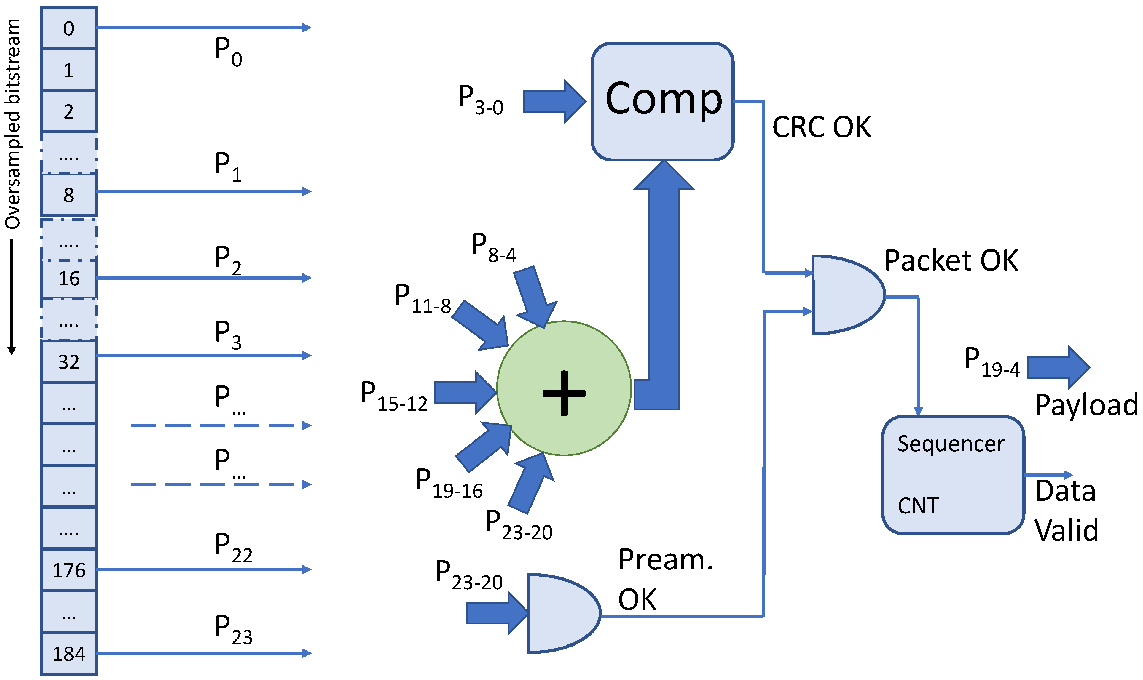
The packet reconstruction block locates the packets in the oversampled bitstream, verifies the checksum, and extracts the payload. Its architecture is detailed in Figure 8.
The oversampled bitstream flows at 1 / T R C rate in a shift-register with 185 flip-flops. From the shift register, the prospective 24-bit packet is extracted in parallel by under-sampling 1 bit every 8 shift positions. For every prospective packet, the preamble is searched in the P23-20 positions with a simple AND gate; the CRC is calculated and compared (COMP) to the sub-word P3-0. If both the aforementioned conditions are true, the sequencer activates the data valid and transfers the payload P19-4 in output. However, since the input bitstream is oversampled, there is the risk that the same packet is detected and outputted up to eight times. For this reason, the sequencer, after a packet is detected, starts a hold-off period where the packet detection is suspended. The packet lasts 24 bits that corresponds to 24 × 8 = 192 T R C ; thus, the hold-off period must last from a minimum of 8 T R C to a maximum of 192 T R C . We used a value of 32   T R C .
The reconstructed packets are finally buffered in a FIFO memory, where they are available for the applications.

4.3. Implementation Performance

The transmitter and receiver described above are implemented in the 10M50DA FPGA of the MAX10 family produced by Intel/Altera. Table 2 reports the resources required by each of the main blocks described in the previous sections for the implementations based on chirps with N S = 56, 112 and 224 samples. The FPGA resources are subdivided in logic cells (LCs), 9k-bit memory blocks (M9ks), and Digital Signal Processors (DSPs), which are hardware multipliers in the 18 × 18 configuration. In the transmitter, the packet formation and serializer blocks require just few LCs, whereas the modulator, as expected, is by far more demanding for resources. Each chirp table, implemented in logics, needs from 120 to 220 LCs, depending on the chirp length. Since in the configuration with N S = 56, 112, and 224 are implemented 7, 14, 28 tables, respectively, the total LCs required by the look-up tables are 840, 2520, 6160 for the 3 different configurations. The complete modulator requires a bit more LCs than those occupied by the look-ups, namely 1137, 4127, and 8120, respectively. Alternatively, we could have implemented the look-up tables in M9k memory resources. However, this is not an efficient solution, since each table stores at maximum 224 × 14 = 3136 bits, whereas the M9k includes 9216 bits with an apparent waste.
In the receiver, the compressor FIR requires from 438 to 1226 LCs, from 3 to 9 memory blocks and from 6 to 24 DSPs. The memories are needed for the realization of the N S -tap data shift register of the FIR; the DSPs are configured like 18 × 18 multipliers. The FIR clock is 125 MHz, i.e., 10-fold the data clock that is 12.5 MHz. The filter has 10 clock cycles for each input data, thus with 6 parallel multipliers it can perform up to 60 multiplications, which is sufficient to cover the 56 multiplications needed for 6. Ns = 56. A similar reasoning applies to the other N S values. The threshold, the sequencer, and the packet reconstruction blocks need few resources. The latter requires a M9k block as well, which implements the shift register.
In summary, the transmitter and receiver require from 2000 to LCs, 4 to 10 memory blocks, and 6 to 24 DSPs, depending on the configuration. The last row of Table 2 shows how these figures compare to the resources of the 10M50 FPGA.

5. Experimental Setup

5.1. The VLC System

The transmitter and receiver described so far have been implemented in a VLC system based on the commercial MAX 10 FPGA development kit produced by Terasic Inc. (Hsinchu County, Taiwan) connected to a custom board designed in our laboratory. The commercial MAX10 kit integrates the 10M50DAF484 FPGA produced by Intel/Altera, and, among other devices, it includes 128 MB of SDRAM, an Ethernet controller, and a HMSC expansion port. The FPGA board, through the HMSC port, is connected to the custom board, which integrates the VLC front-end. Once connected, these two boards represent the VLC system sketched in Figure 9.
In transmission, the FPGA synthesizes the signal and drives a Digital-to-Analog converter (DAC) that features a 14-bit resolution and works up to 125 Msps. The converted signal feeds a transconductance amplifier capable of generating up to ±1 A, similar to those employed in ultrasound [28]. This current is added to a constant current source of up to 1 A, and the resulting current powers an external LED.
In reception, the custom board receives the signal from an external photodetector. A Low Noise Amplifier (LNA) processes the signal before it feeds an Analog-to-Digital converter (ADC) capable of 12-bit at 40 Msps that here is employed at 12.5 Msps. The input noise is minimized also by synchronizing the switching power supplies of the VLC system to the bit rate [29].
The VLC system connects through the Ethernet link to a host PC where a MATLAB interface runs. This interface is used to set the working parameters and monitor the system during the experiments.

5.2. Experimental Set-Up

The experimental set up was arranged like shown in Figure 10a. The VLC system, detailed in Figure 10b, was connected in transmission to the commercial white (5000 K) LED module for ambient lightening XHP50 (Cree Inc. Durham, NC, USA). It is actually composed by four LED cells connected in series on the die. It supports a current up to 1.5 A with a voltage drop of about 12 V. This LED exploits yellow phosphorous for generating the white light, and, in general, it is known that this technology features a bandwidth limited to a few MHz [14]. We characterized this LED with a preliminary experiment, and we found a 1.8 MHz bandwidth at −3 dB. The transmitter was set to produce a 1 A continuous current with added a modulation current of ± 0.25 A. The DA converter worked at 12.5 Msps.
In reception, we used the PDAPC2 photodetector from Thorlab Inc., (Newton, NJ, USA). It features a programmable gain that we set at 0 dB to obtain a 11 MHz bandwidth (at higher gain the bandwidth reduces). The PDAPC2 was placed in front of a LED on a tripod, so that the LED-detector distance can be easily changed. The signal from the photodetector was monitored in an oscilloscope (see Figure 10a) and delivered to the VLC system input (see Figure 10b). The LNA of the custom board was set for 30 dB gain, and the following AD converter was set for 12.5 Msps. The setup was completed by a power unit that powered the VLC system and a PC connected through Ethernet to the system. Table 3 summarizes the experimental parameters.

6. Measurements and Results

6.1. Communication Distance and Packet Error Rate

The set-up described in the previous section was used for measuring the Packet Error Rate (PER) at increasing distances. In particular, the 3 chirps of Table 1 were tested over the communication distances from 1.5 m to 4.0 m. For each experiment, at least 1 M packets were sent, corresponding to 1 M × 24 = 24 M bits. Since the communication rate was 1 / T B = 1.5625 Mb/s, each experiment lasted about 15 s. The PER was automatically calculated in the FPGA by counting the transmitted packets and the packets received with no errors. Figure 11 reports the measurements.
For distances below 180 cm, no errors were measured for any of the 3 chirps in the 1 M packets sent, corresponding to a PER < 10−6 (or a BER < 4∙10−8). At a distance between 180 and 215 cm, the errors measured for the chirp with T = 4.48 µs started to increase, whereas the other 2 chirps produced no errors. At a distance between 215 and 280 cm, the errors measured for the chirp with T = 8.96 µs started to increase as well, whereas the longest chirp continued to produce no errors. Finally, at distances higher than 280 cm, the longest chirp also produced increasing errors, although the PER was still below 10−1 up to 340 cm.
In order to quantitatively compare the performance of the 3 chirps, we set a threshold, for example, at PER = 0.05 (see the red line in Figure 11). At this PER, we measured a communication distance of 212, 253, 320 cm for the 3 chirps, respectively. From these data, we can now calculate the gain in communication distance that we obtain by increasing the chirp temporal duration and compare this to its theoretical trend given by (5). It is useful to nominate the 3 chirps T17.92, T8.96, T4.48, where the subscript reports the respective chirp temporal duration. If N is the ratio between chirp durations, see (5), we can compare T17.92 against T8.96 (N = 2); T17.92 against T4.48 (N = 4), and T8.96 against T4.48 (N = 2), for a total of 3 comparisons. For example, the length ratio between chirps T17.92 and T8.96 is N = 17.92/8.86 = 2, and we measured a distance gain of 320/253 ≈ 1.26. The experimental data are represented by the red diamond, yellow cross, violet circle markers in Figure 12, which reports N along the x-axis and the distance gain along the y-axis. These data are compared to the theoretical gain in distance achievable by stretching the chirp duration, i.e., the blue curve given by (5). For example, in the case of T17.92 against T8.96 we measured a 320/253 ≈ 1.26 gain (yellow cross) to be compared to the theoretical 1.2 (blue line at N = 2).

6.2. Latency and Throughput

The latency was evaluated by measuring the time needed by the 16-bit payload to travel from the input of transmitter FIFO (see Figure 5) to the output of the receiver FIFO (see Figure 7). This time includes several steps of transmission-reception path: TX digital processing (packetization, serialization, chirp modulation), the pipelines of the DA converter, the delay of the analog amplifier, the time-of-flight, the delay of the photodetector and analog amplification, the pipeline of the AD converter, and finally the receiver digital processing (compressor filter, thresholding, packet reconstruction). The total delay is clearly dominated by the time required for the digital TX/RX processing, whereas the delays of the analog circuits and the time-of-flight can be neglected.
Table 4 and Figure 13 details the delay of each of the digital blocks involved in the processing (see Figure 5 and Figure 7). Let us start the description with the transmitter, which is clocked at 1/ T T C = 12.5 MHz. At time t = 0, the 16-bit payload is uploaded in TX FIFO. The data exit the FIFO in 2 clock cycles (T1 in Figure 13), and the 24-bit packet is formatted in 4 clock cycles (T2 in Figure 13). The packet serialization takes 24 · T B = 15.36 µs, from T2 to T5 in Figure 13. This relative long time is due to the modulator that accepts in input new bits at the transmission rate, i.e., 1/ T B . The first bit is available at the modulator input as soon as the packet is ready (T2), and the corresponding chirp starts to be transmitted after 4 clock cycles (T3). The modulator continues to transmit the data, until the last chirp corresponding to the last bit is out (T6). The transmission in air of the packet lasts 23× T B + T, where T is the chirp length. In summary (see Table 4), the packet is in air 0.8 µs after the payload is fed in the FIFO, and the transmission ends in 15.52 + T µs, where T is the length of the chirp employed in the modulation.
Neglecting the small delays due to the analog circuits and the time-of-flight, the modulated data packet is present at the receiver input in the time range T3–T6. The receiver works with a 125 MHz clock. The first compressed pulse is present in output when the first chirp is completely inside the compressor, plus 16 clock cycles of internal latency (see T4); the last compressed pulse is on output when the last chirp is inside, i.e., 24 · T B = 12.36 µs later. The thresholding, the packet recognition, and the FIFO add two clock cycles each. In summary (see Table 4), in case no transmission errors occur, the 16-bit payload is available at the FIFO RX output 16.336 µs + T after it was fed to the FIFO TX, which corresponds to less than 21, 24, 37 µs for the 3 chirps tested.

7. Discussion

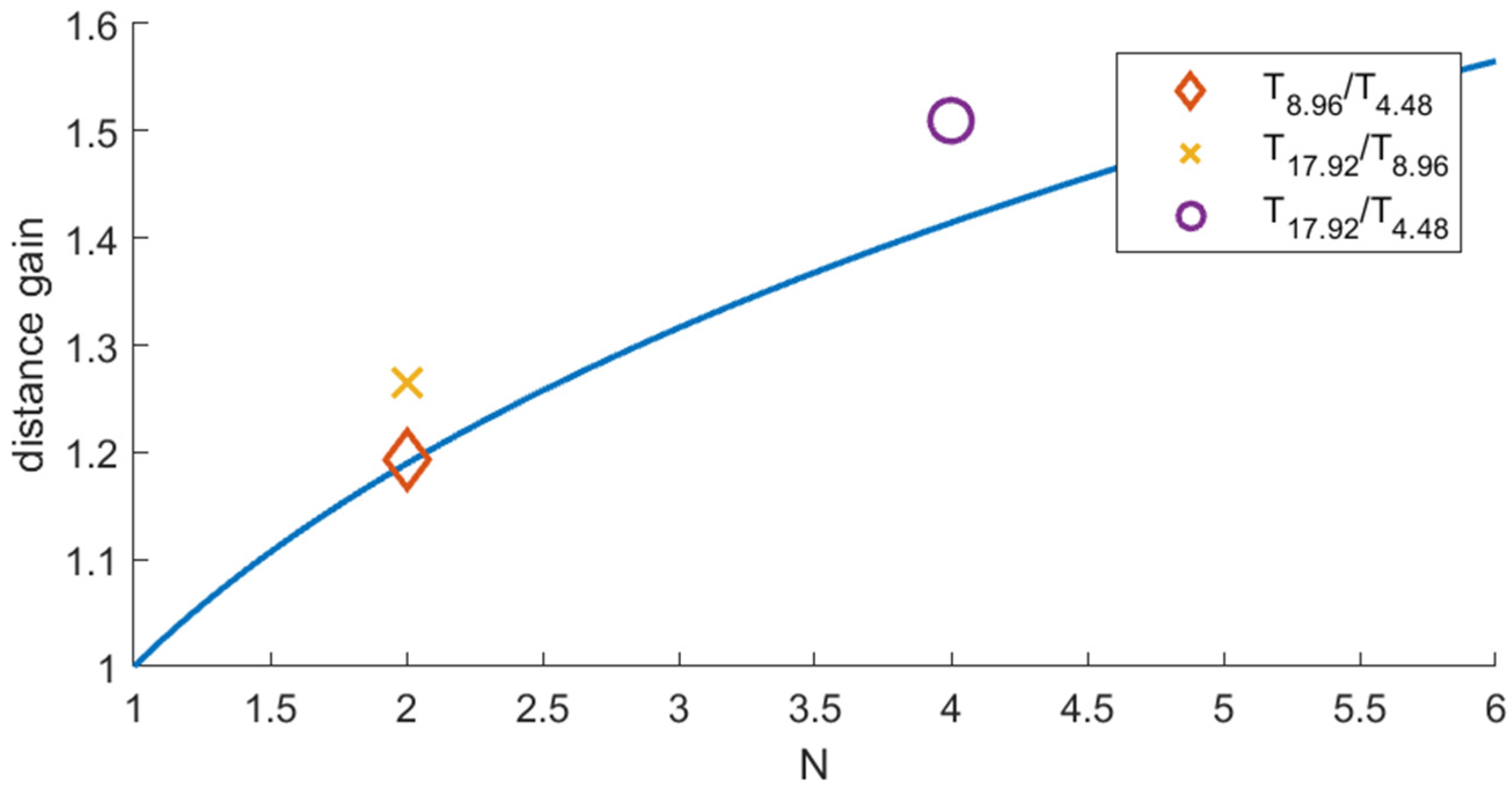
In this paper, the possibility of employing the chirp coding in VLC has been investigated and the performance of different chirp codes has been compared. The experiments confirmed (see Figure 12) that the gain in communication distance achieved by different chirp temporal durations well fits the theoretical trend, given by (5). These results prove that the advantages of chirp modulation, which made this technique widely employed in other fields like radar and sonar, can be exploited in VLC as well. The SNR gain achievable by chirp modulation and pulse compression is related to the chirp temporal length, not to the chirp amplitude [22,23]. Communications at increasing distances can be obtained by employing chirp at increasing lengths, or low-energy links can be obtained by reducing the chirp amplitude and compensating by increasing its length.
However, for chirp modulation to have practical applications, it is necessary to demonstrate the feasibility of its real-time, low-latency implementation. In this work we shown an FPGA real-time implementation with a latency below 40 µs, suitable to satisfy even the most severe requirements of the current and next-future applications, like for example the industrial environment [11] and motor control loops [30]. The high calculation requirements of the pulse compressor are satisfied in real-time and ultra-low-latency environments by FPGAs only. However, different approaches are possible. For example, a processor can execute the same calculations with a higher latency and a lower throughput. On the other hand, the availability of the FPGA opens the possibility of applying in real-time, with a small latency cost, correction algorithms like Reed-Solomon [31], Viterbi [32], or others that can improve the robustness of the communication.
The aim of the presented experiments was not to stress for the maximum achievable distance or data rate. The communication distance can be further improved, for example, by increasing the optical gain with a lamp deflector and/or a lens at the receiver [33]. On the other hand, in chirp modulation the bit rate is limited by the compressed pulse resolution W, that, in turn, is constrained by the chirp bandwidth. In these experiments we exploited all of the bandwidth available from the employed LED (about 1.8 MHz). Different LED technologies (e.g., non-phosphorous based) or the use of blue filters allow a higher bandwidth [34], but this is typically achieved at the detriment of the received power.

8. Conclusions

This paper shows that the positive SNR features of chirp modulation and pulse compression can be exploited in VLC as well, like demonstrated by the ultra-low latency implementation of a 1.56 Mb/s link. These results open the possibility of a practical exploitation of VLC links in low-energy and/or high-distance applications.

Author Contributions

Conceptualization, S.R. and L.M.; software, S.R.; formal analysis, S.C.; investigation, S.R. and S.C.; resources, S.R. and L.M.; writing—original draft preparation, S.R.; writing—review and editing, S.C. and L.M.; funding acquisition, S.R. and L.M. All authors have read and agreed to the published version of the manuscript.

Funding

This research is partially funded by the Ministry of Education, University and Research (MIUR) of the Italian government.

Data Availability Statement

Data is contained within the article.

Conflicts of Interest

The authors declare no conflict of interest.

References

  1. Khan, L.U. Visible Light Communication: Applications, Architecture, Standardization and Research Challenges. Digit. Commun. Netw. 2017, 3, 78–88. [Google Scholar] [CrossRef] [Green Version]
  2. Rehman, S.; Ullah, S.; Chong, P.; Yongchareon, S.; Komosny, D. Visible Light Communication: A System Perspective—Overview and Challenges. Sensors 2019, 19, 1153. [Google Scholar] [CrossRef] [Green Version]
  3. Li, H.; Chen, X.; Huang, B.; Tang, D.; Chen, H. High Bandwidth Visible Light Communications Based on a Post-Equalization Circuit. IEEE Photon. Technol. Lett. 2014, 26, 119–122. [Google Scholar] [CrossRef]
  4. Kavehrad, M. Optical Wireless Applications: A Solution to Ease the Wireless Airwaves Spectrum Crunch; Dingel, B.B., Jain, R., Tsukamoto, K., Eds.; SPIE: San Francisco, CA, USA, 2013. [Google Scholar] [CrossRef]
  5. Elgala, H.; Mesleh, R.; Haas, H. Indoor Optical Wireless Communication: Potential and State-of-the-Art. IEEE Commun. Mag. 2011, 49, 56–62. [Google Scholar] [CrossRef]
  6. Ndjiongue, A.R.; Ferreira, H.C. An Overview of Outdoor Visible Light Communications: An Overview of Outdoor Visible Light Communications. Trans. Emerg. Telecommun. Technol. 2018, 29, e3448. [Google Scholar] [CrossRef]
  7. Dhatchayeny, D.R.; Sewaiwar, A.; Tiwari, S.V.; Chung, Y.H. Experimental Biomedical EEG Signal Transmission Using VLC. IEEE Sensors J. 2015, 15, 5386–5387. [Google Scholar] [CrossRef]
  8. De Marcellis, A.; Di Patrizio Stanchieri, G.; Faccio, M.; Palange, E.; Constandinou, T. A 300 Mbps 37 PJ/Bit UWB-Based Transcutaneous Optical Biotelemetry Link. IEEE Trans. Biomed. Circuits Syst. 2020, 14, 441–451. [Google Scholar] [CrossRef]
  9. Liang, Q.; Sun, Y.; Liu, C.; Liu, M.; Wang, L. LedMapper: Toward Efficient and Accurate LED Mapping for Visible Light Positioning at Scale. IEEE Trans. Instrum. Meas. 2022, 71, 1–12. [Google Scholar] [CrossRef]
  10. Seminara, M.; Meucci, M.; Tarani, F.; Riminesi, C.; Catani, J. Characterization of a VLC System in Real Museum Scenario Using Diffusive LED Lighting of Artworks. Photon. Res. 2021, 9, 548. [Google Scholar] [CrossRef]
  11. Almadani, Y.; Plets, D.; Bastiaens, S.; Joseph, W.; Ijaz, M.; Ghassemlooy, Z.; Rajbhandari, S. Visible Light Communications for Industrial Applications—Challenges and Potentials. Electronics 2020, 9, 2157. [Google Scholar] [CrossRef]
  12. Cailean, A.-M.; Dimian, M. Current Challenges for Visible Light Communications Usage in Vehicle Applications: A Survey. IEEE Commun. Surv. Tutor. 2017, 19, 2681–2703. [Google Scholar] [CrossRef]
  13. Gagliardi, R.M.; Karp, S. Optical Communications. In Wiley Series in Telecommunications and Signal Processing, 2nd ed.; Wiley: New York, NY, USA, 1995; ISBN 978-0-471-54287-2. [Google Scholar]
  14. Li, H.; Chen, X.; Guo, J.; Chen, H. A 550 Mbit/s Real-Time Visible Light Communication System Based on Phosphorescent White Light LED for Practical High-Speed Low-Complexity Application. Opt. Express 2014, 22, 27203. [Google Scholar] [CrossRef] [PubMed] [Green Version]
  15. Chang, Y.-H.; Huang, Y.-M.; Liou, F.-J.; Chow, C.-W.; Liu, Y.; Kuo, H.-C.; Yeh, C.-H.; Gunawan, W.H.; Hung, T.-Y.; Jian, Y.-H. 2.805 Gbit/s High-Bandwidth Phosphor White Light Visible Light Communication Utilizing an InGaN/GaN Semipolar Blue Micro-LED. Opt. Express 2022, 30, 16938. [Google Scholar] [CrossRef] [PubMed]
  16. Cossu, G.; Khalid, A.M.; Choudhury, P.; Corsini, R.; Ciaramella, E. 34 Gbit/s Visible Optical Wireless Transmission Based on RGB LED. Opt. Express 2012, 20, B501. [Google Scholar] [CrossRef]
  17. Nawaz, T.; Seminara, M.; Caputo, S.; Mucchi, L.; Cataliotti, F.S.; Catani, J. IEEE 802.15.7-Compliant Ultra-Low Latency Relaying VLC System for Safety-Critical ITS. IEEE Trans. Veh. Technol. 2019, 68, 12040–12051. [Google Scholar] [CrossRef] [Green Version]
  18. Klauder, J.R.; Price, A.C.; Darlington, S.; Albersheim, W.J. The Theory and Design of Chirp Radars. Bell Syst. Tech. J. 1960, 39, 745–808. [Google Scholar] [CrossRef]
  19. Ramalli, A.; Boni, E.; Dallai, A.; Guidi, F.; Ricci, S.; Tortoli, P. Coded Spectral Doppler Imaging: From Simulation to Real-Time Processing. IEEE Trans. Ultrason. Ferroelectr. Freq. Control. 2016, 63, 1815–1824. [Google Scholar] [CrossRef]
  20. Rudys, S.; Ragulis, P.; Laučys, A.; Bručas, D.; Pomarnacki, R.; Plonis, D. Investigation of UAV Detection by Different Solid-State Marine Radars. Electronics 2022, 11, 2502. [Google Scholar] [CrossRef]
  21. Ricci, S.; Meacci, V. Data-Adaptive Coherent Demodulator for High Dynamics Pulse-Wave Ultrasound Applications. Electronics 2018, 7, 434. [Google Scholar] [CrossRef]
  22. Ducoff, M.R.; Tietjen, B.W. Pulse compression radar. In Radar Handbook, 3rd ed.; Skolnik, M.I., Ed.; McGraw-Hill: New York, NY, USA, 2008; ISBN 978-0-07-148547-0. [Google Scholar]
  23. He, H.; Li, J.; Stoica, P. Waveform Design for Active Sensing Systems: A Computational Approach; Cambridge University Press: Cambridge, UK; New York, NY, USA, 2012; ISBN 978-1-107-01969-0. [Google Scholar]
  24. Golomb, S.W.; Gong, G. Signal Design for Good Correlation: For Wireless Communication, Cryptography, and Radar; Cambridge University Press: Cambridge, UK, 2005; ISBN 9780521821049. [Google Scholar]
  25. Caputo, S.; Mucchi, L.; Cataliotti, F.; Seminara, M.; Nawaz, T.; Catani, J. Measurement-Based VLC Channel Characterization for I2V Communications in a Real Urban Scenario. Veh. Commun. 2021, 28, 100305. [Google Scholar] [CrossRef]
  26. Avalon® Interface Specifications, MNL-AVABUSREF 24 January 2022. Available online: https://www.intel.com/content/www/us/en/docs/programmable/683091/22-3/introduction-to-the-interface-specifications.html (accessed on 22 December 2022).
  27. FIR II IP Core User Guide, UG01072, 12 June 2020. Available online: https://www.intel.com/content/www/us/en/docs/programmable/683208/17-1/about-the-fir-ii-ip-core.html, (accessed on 22 December 2022).
  28. Ricci, S.; Russo, D. Linear Ultrasound Transmitter Based on Transformer with Improved Saturation Performance. Electronics 2021, 10, 107. [Google Scholar] [CrossRef]
  29. Ricci, S. Switching Power Suppliers Noise Reduction in Ultrasound Doppler Fluid Measurements. Electronics 2019, 8, 421. [Google Scholar] [CrossRef] [Green Version]
  30. Ricci, S.; Meacci, V. Simple Torque Control Method for Hybrid Stepper Motors Implemented in FPGA. Electronics 2018, 7, 242. [Google Scholar] [CrossRef] [Green Version]
  31. Wicker, S.B.; Bhargava, V.K. Reed–Solomon Codes and Their Applications; Wiley-IEEE Press: Piscataway, NJ, USA, 1994; ISBN 978-0-7803-5391-6. [Google Scholar]
  32. Viterbi, A. Error Bounds for Convolutional Codes and an Asymptotically Optimum Decoding Algorithm. IEEE Trans. Inform. Theory 1967, 13, 260–269. [Google Scholar] [CrossRef] [Green Version]
  33. Nawaz, T.; Seminara, M.; Caputo, S.; Mucchi, L.; Catani, J. Low-Latency VLC System with Fresnel Receiver for I2V ITS Applications. J. Sens. Actuator Netw. 2020, 9, 35. [Google Scholar] [CrossRef]
  34. Wang, S.-W.; Chen, F.; Liang, L.; He, S.; Wang, Y.; Chen, X.; Lu, W. A High-Performance Blue Filter for a White-Led-Based Visible Light Communication System. IEEE Wirel. Commun. 2015, 22, 61–67. [Google Scholar] [CrossRef]
Figure 1. Example of chirp with T = 10 µs, B = 4 MHz, BT = 40 and its compressed pulse. (a) Chirp signal; (b) instantaneous frequency of the chirp; (c) spectrum of the chirp; (d) compressed pulse with −4 dB width W = 0.25 µs and amplitude gain A = 6.3.
Electronics 12 00364 g001
Figure 2. Example of the modulation scheme. The R F t x n (bottom) is obtained by summing up the chirps delayed by T B and zeroed for ‘0’ bits. Here the arbitrary 14-bit sequence “11011101011011” is transmitted with LSB first.
Electronics 12 00364 g002
Figure 3. Format of the 24-bit data packet P23-0. It is composed by the CRC C3-0, the payload W15-0, and the fixed preamble “1111”.
Electronics 12 00364 g003
Figure 4. The received signal (top) is correlated to the chirp to obtain the compressed signal (bottom). The bitstream is recovered by detecting the peaks through a threshold (red dashed line). In this example, the 24-bit packet “111101011101001110010100” is detected.
Electronics 12 00364 g004
Figure 5. Architecture of the transmitter.
Electronics 12 00364 g005
Figure 6. Architecture of the modulator.
Electronics 12 00364 g006
Figure 7. Architecture of the receiver.
Electronics 12 00364 g007
Figure 8. Architecture of the packet reconstruction block integrated in the receiver.
Electronics 12 00364 g008
Figure 9. The VLC system based on the MAX10 developing kit and the custom board.
Electronics 12 00364 g009
Figure 10. (a) Experimental setup composed by the VLC system, the host PC where the MATLAB interface runs, a power unit, an oscilloscope, the XHP50 LED, and the PDAPC2 detector held by a tripod. (b) Detail of the VLC system: the VLC custom board and the FPGA board are visible on the top and bottom, respectively.
Electronics 12 00364 g010
Figure 11. PER measured at different communication distances with the 3 chirps of T = 4.48 (violet), T = 8.96 (green), T = 17.92 (light blue). Blue marks represent the measurement points.
Electronics 12 00364 g011
Figure 12. Theoretical (light blue curve) and measured (markers) distance gain towards chirp stretching. N represents the ratio between chirps' temporal durations.
Electronics 12 00364 g012
Figure 13. Delays (not to scale for clarity) in the TX and RX processing chain. The time-bars referrer to the output of the corresponding block.
Electronics 12 00364 g013
Table 1. Features of the chirps.
ParameterChirp 1Chirp 2Chirp 3
B1.7 MHz1.7 MHz1.7 MHz
F M i n 100 kHz100 kHz100 kHz
F M a x 1.8 MHz1.8 MHz1.8 MHz
T 4.48 µs8.96 µs17.92 µs
BT6.813.627.2
W588 ns588 ns588 ns
T T C 80 ns80 ns80 ns
N S 56112224
Table 2. Resources of MAX10 FPGA employed by the transmitter and receiver.
NS = 56 SampleNS = 112 SampleNS = 224 Sample
LCsM9ksDSPs
(18 × 18)
LCsM9ksDSPs
(18 × 18)
LCsM9ksDSPs
(18 × 18)
Transmitter
Packet formation930093009300
Serializer120012001200
Modulator113700412700812000
    Chirp table    120    0    0    180    0    0    220    0    0
Sub-total124200423200822500
Receiver
Compressor FIR438367105121226924
Threshold500500500
Packet501050105010
Sequencer200020002000
Sub-total5134678561213011024
TOT175546501761295261024
% (10M50)3.5%2.2%4.2%10.1%3.3%8.4%19.1%5.5%16.8%
Table 3. Parameters of the experimental set-up.
ParameterValue
Transmitter
LED modelXHP50 (5000 K, Cree Inc.)
LED mean current1 A
Modulation current±0.25 A
LED bandwidth1.7 MHz (−3 dB), 2 MHz (−3.4 dB)
DAC14-bit, 12.5 Msps
Receiver
PhotodetectorPDAPC2 (Thorlab Inc.)
Bandwidth11 MHz (0 dB), 1.4 MHz (10 dB)
LNA gain30 dB
ADC12-bit, 12.5 Msps
Table 4. FPGA delays in TX-RX data path.
StepTimeTime Ref
Payload at FIFO input00
TX FIFO out0.16 µsT1
Packet Formation0.48 µsT2
Serializer0.48 µs − 15.84 µsT2–T5
Modulator Out0.80 µs − 15.52 µs + TT3–T6
Receiver input0.80 µs − 15.616 µs + TT3–T6
Compressor filter outT + 1.024 µs − T + 16.288 µsT3–T7
Thresholds outT + 16.304 µsT8
Packet recog. outT + 16.320 µsT9
RX FIFO outT + 16.336 µsT10
Disclaimer/Publisher’s Note: The statements, opinions and data contained in all publications are solely those of the individual author(s) and contributor(s) and not of MDPI and/or the editor(s). MDPI and/or the editor(s) disclaim responsibility for any injury to people or property resulting from any ideas, methods, instructions or products referred to in the content.

