Article

A 100-Gb/s PAM-4 DSP in 28-nm CMOS for Serdes Receiver

1
Institute of Microelectronics of the Chinese Academy of Sciences, Beijing 100029, China
2
Institute of Computing Technology Chinese Academy of Sciences, Beijing 100190, China
3
Wuxi Institute of Interconnect Technology, Wuxi 214105, China
*
Author to whom correspondence should be addressed.
Electronics 2023, 12(2), 257; https://doi.org/10.3390/electronics12020257
Submission received: 18 November 2022 / Revised: 21 December 2022 / Accepted: 27 December 2022 / Published: 4 January 2023

Abstract

:
This paper presents a dedicated digital signal process (DSP) for four pulse amplitude modulation (PAM4) SerDes receivers. It is targeted to implement data recovery and adaptive equalization under ultra-high-speed and large channel attenuation with a small area and high power efficiency. The DSP consists of a clock data recovery (CDR), a 16-tap feed forward equalizer (FFE), a 1-tap decision feedback equalizer (DFE), and an automatic adaptation engine. An adaptive least mean square (LMS) algorithm is utilized to make the system more intelligent in calculating tap coefficients of the FFE and DFE. To address the timing limitation associated with traditional digital DFE that cannot handle large amounts of parallel data at a high speed, speculative techniques and a customized 4-to-1 multiplexer (MUX) unit are employed to remove the summation time and reduce the selection time, respectively. A first-order sigma-delta modulator is used to replace the traditional moving average to calculate average voltages, which could prominently save the hardware resources and power consumption. Additionally, the influence of input quantization resolution on the equalization ability is analyzed. Implemented in a 28-nm CMOS, the DSP could compensate for up to 33-dB loss at 100 Gb/s with a power consumption of 7.22 pJ/bit.

1. Introduction

With the data explosion in cloud computing, 5G networking, industrial IoT, and media sharing, the line rate of high-speed serial links has been improved to 56–112 Gb/s, Serializer-Deserializer (Serdes) has become a mainstream communication technology due to its full utilization of channel capacity, fewer device pins and faster transmission speed, while four-pulse amplitude modulation (PAM4) has become a mainstream modulation scheme due to its high spectral efficiency. Benefitting from the development of the CMOS technology, the digital signal process (DSP)-based equalization has become an indispensable component target to compensate for the severe channel attenuation [1]. However, the DSP faces the problems of insufficient compensation ability, massive power consumption, and excessive area occupation. These problems could become more severe as the data rate increases.
Therefore, how to recover the signal efficiently and quickly is particularly important. The encoding of 4 Pulse Amplitude Modulation (PAM4) for two bits on each symbol is a prominent advantage compared with Not Return to Zero (NRZ). However, compared with NRZ mode, the eye-opening and linearity of data transmission in PAM4 mode are significantly reduced. In order to meet the strict requirements of eye-opening and linearity, a powerful equalizer structure is required [2]. The receiver base of an analog-to-digital converter (ADC) improves this situation nicely [3]. And the fully digital equalizer (feed forward equalizer (FFE), decision feedback equalizer (DFE)) based on ADC has begun to be proposed. However, SerDes receivers have high requirements on the DSP, such as strong equalization capability, low power consumption, and small area [4].
In this paper, we design a DSP module suitable for ADC+DSP architecture of Serdes receiver, which has high speed, low bit error rate (BER) and other advantages. In this design, least mean square (LMS) algorithm is adopted to provide coefficients to FFE and DFE modules in DSP adaptively, so that the system can balance channels with different attenuations adaptively. In order to reduce the overall power consumption of the system, some optimization is made in the process of implementing LMS algorithm without affecting the overall performance [5]. In this paper, DSP is mainly used to compensate for large mchannel attenuation (maximum −33 dB). In the implementation process of DSP, the first-order sigma-delta integrator is used to replace the traditional division for average operation, which can optimize the power consumption and area of the system. At the same time, the optimal truncation program would be discussed under the condition of equilibrium intensity and high speed. Besides, the problem of a tense time in traditional DFE was solved by implementing a 1-tap speculative DFE and customized 4-to-1 multiplexer (MUX) unit, and the impact of ADC output width also will be discussed to provide a reference for the design of ADC [6]. Finally, a DSP module with a speed of 100 Gb/s and a maximum attenuation of −33 dB is realized on the 28 nm process node. After silicon test, the BER is 1 × 10 8 and the power consumption is 7.22 pJ/bit in a 50 cm channel.
The rest of the paper is organized into three sections. Section 2 describes the Architecture of DSP. Section 3 covers the Crucial Techniques. Section 4 cover Layout Implementation and Verification Results. The final summary and conclusion are presented in Section 5.

2. Architecture of DSP

Figure 1 shows the block diagram of the implemented DSP. It contains a clock data recovery (CDR) engine, a 16-tap FFE, a 1-tap DFE, and two LMS engines. The system mainly consists of two parts. One is the data path, which is composed of FFE and DFE in series and is used to balance the received data so as to recover a clear eye map [7]. The tap coefficients of FFE and DFE are provided by their respective LMS algorithms to achieve the purpose of adaptive balancing. The other part is the clock recovery pathway, which is implemented by the CDR module. It is used to process the received data so as to recover the correct sampling points, and then feed back to the ADC for sampling [8]. A small FFE module is integrated internally to provide the variables required by the algorithm to the CDR module. As shown in Figure 1, the quantized 8-bit data of the ADC are respectively applied to the CDR and FFE, where the former is adopted to adjust the sampling clock to its optimal point using a Mueller Mueller phase detector (MM-PD), and the latter is employed to compensate for the long-tail inter symbol interference (ISI). In particular, the CDR adopts a simplified 8-tap FFE data path instead of the 16-tap data path in the FFE structure, so that the phase information can be output as soon as possible in order to reduce the loop delay, thereby optimizing the bandwidth and phase margin of the CDR. The putative 1-tap DFE is linked to the FFE output to make further data balancing and data decisions. The 16-tap FFE and 1-tap DFE utilize separate LMS engines to continuously update the tap weights, where the bandwidth of the DFE loop is designed to be much smaller than the FFE loop to ensure their convergence [9].

3. Crucial Techniques

3.1. High-Speed Techniques

There are two difficulties in the design of 100 Gb/s DSP. One of the difficulties is the strict timing of the DFE structure. The data input in parallel must be processed and output in one cycle, so as to ensure that the parallel data of the next cycle can be connected when it arrives. This means that the time required for each DFE to process a channel of data is actually less than or equal to the symbol width (20 ps for 100 Gb/s PAM4 modulation). Another difficulty of DSP is the 16-tap FFE structure because its final output is composed of each tap data and their corresponding tap weights multiplied and then added, so this problem can be solved by inserting enough registers [10]. However, an FFE with a 16-tap structure needs to insert 15 registers. For parallel data, the number of registers that need to be inserted will be more, which will make the delay in obtaining the result of the FFE very long, and its occupied area and power consumption will also be larger. These are all things that need to be avoided in high-speed, low-power designs. This section aims to address these two problems by developing FFE structures for parallel operations, speculative DFEs with custom MUXs, and optimizing them with some low-power algorithms during data processing.

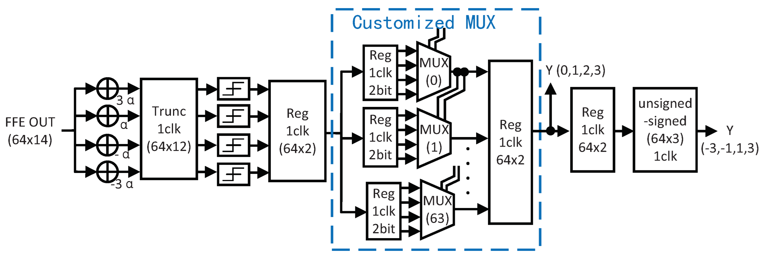
3.1.1. Speculative DFE with Customized MUX

Figure 2 shows the simplified diagram of the 64-way parallel 1-tap speculative DFE. Compared with the expanded DFE design [3], it removes the multiplication, summation, and decision unit of the first tap and its coefficients from the feedback loop. These three units are then copied into four copies (there are only four decisions) and placed at the data entry. When each data period comes, it first calculates the four decision results separately to get the new four decision results. These results are then selected to obtain the final output, which is more suitable for high-speed circuits and parallel data links. Figure 3 visually shows the timing propagation diagram of the speculative DFE. The output of each MUX depends on the selection result of its previous data [11], so the selection process of this parallel data should be completed within one clock cycle. This means the selection for each MUX should be finished in one symbol width [8]. For the 100 Gb/s PAM4 (i.e., the symbol width equals 20 ps), the selection-to-data (S-to-D) delay of each MUX (i.e., shown in Figure 2) should be less than 20 ps. However, the standard MUX for 28-nm CMOS is around 40 ps, which cannot satisfy the timing requirements. To solve this problem, a customized MUX shown in Figure 4 is adopted. The S-to-D delay consists of the delay of two transmission gates and two inverters. The simulation results show that the maximum S-to-D delay of the customized MUX is around 16 ps, which can satisfy the timing requirement.

3.1.2. Fixed-Point Operation Strategy

The implementation of traditional FFE involves multiplication, addition, and delay logic. This process requires consideration of speed and accuracy [6]. The more the number of taps, the more registers it needs, and the longer the calculation time will be. Moreover, the coefficients involved in the calculation process are floating decimal, and the balance between speed and accuracy needs to be considered in the design.
This design adopts a fixed-point operation strategy to solve the above problems. The strategy adopts a parallel FFE structure, that is, each clock cycle reorganizes the input 64-way of parallel data with the parallel data of the previous cycle and the next cycle, and then splits it into a 64 × 16 data matrix. Multiply this matrix with the coefficients corresponding to the 16 taps, and then add them to get the 64-way output of the FFE. Figure 5 shows the block diagram of the developed parallel FFE, where the FFE contains 8 pre taps and 7 post taps. Here, the bit numbers of the tap coefficients are chosen to be 9 bits to balance the speed and accuracy. To implement the multiplication and summation of the FFE, the 8-bit input data is extended to 21 bits by amplifying 9 bits and adding a 4-bit sign bit in the high order. After the multiplication and summation of the FFE, the lower 7 bits are first truncated to obtain the FFE output, leaving a 2-bit margin to maintain acceptable precision for DFE processing. After DFE processing, the lowest two bits will be further truncated to obtain the final equalized data with the same scale as the input data.
Figure 6 shows the simulated eye map of FFE with different coefficient accuracies at 64 Gb/s. The channel loss at the Nyquist frequency is around 23 dB. Figure 6a,b compare the eye diagrams of FFE based on the fixed-point operation (9-bit coefficients) in hardware implementation and FFE based on floating-point operation in Matlab. It can be seen that the FFE based on fixed-point operation shows acceptable performance degradation. It can be seen that the 9-bit-coefficient FFE shows acceptable performance degradation. Figure 6c,d further show the simulated eye diagrams when applying 8-bit and 10-bit-coefficient FFE. As can be observed, the 10-bit-coefficient FFE shows ignorable improvement in contrast to the 9-bit one while the 8-bit coefficient FFE/DFE exhibits a visible deterioration.
Moreover, Table 1 shows the vertical eye closure (VEC) and vertical eye-opening ratio (VEOR) [12] corresponding to Figure 6a,c,d. The VEC is defined as 20log 10 (AV u p p /V u p p ) m a x , where the AV u p p is the amplitude of the eye and the V u p p is the eye height. And the VEOR is defined as −20log 10 ( (v − 1)/v), where the v = 10 V E C / 20 . Based on these simulation results, the 9-bit fixed-point operation is adopted in this design.

3.2. Lower-Power Techniques

The power consumption of the DSP is mainly in the calculation of the FFE/DFE data paths and their tap coefficients. The aforementioned optimization of word length is naturally a method to balance data path performance and power consumption. In order to further reduce the power consumption of this system, this section will introduce two techniques to further optimize power consumption. One is to develop an LMS algorithm based on random selection, which enables it to reduce the power consumption of the tap weight calculation with negligible performance degradation. Another is to replace the traditional moving average filter with an average calculator based on the sigma-delta algorithm to significantly reduce the averaging hardware.

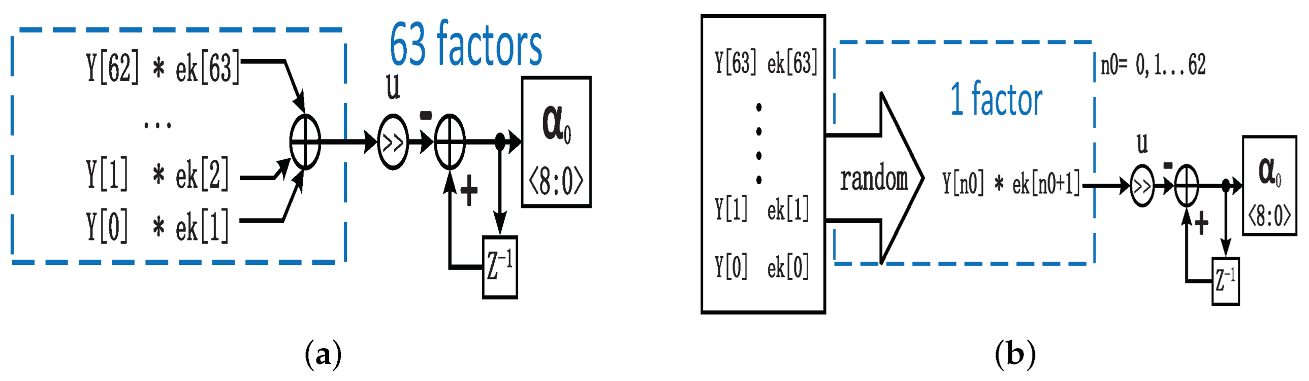
3.2.1. Random-Data-Selection-Based LMS Implementation

The LMS adaptive FFE coefficient could be calculated by the following equation [4], Equation (1) is in the Appendix A:
W ( n ) = W ( n 1 ) + 2 μ e k ( n ) Y ( n )
where Y(n) is the judgment result of the 64-way DFE, ek(n) is the error of the actual value of the 64-way data relative to its ideal value, W(n) is the current cycle tap coefficient vector, and W(n − 1) is a vector of tap coefficients for the previous cycle. Figure 7 and Figure 8 shows traditional LMS implementation in FFE and DFE, which utilizes all parallel data to perform the tap coefficient calculation. This full parallel data processing can quickly and accurately collect residual ISI for each tap, hence supporting a fast convergence speed. In practice, the convergence speed is not a critical parameter as the channel loss usually varies very slowly for wireline systems. Based on this observation, we propose an LMS algorithm based on random data selection (see Figure 7 and Figure 8), where the data applied to the LMS engine is selected from parallel data by a pseudo-random algorithm. Using the above random data selection idea, in the LMS algorithm of FFE, 4 data are randomly selected from 49 data and substituted into Equation (1) for calculation. Similarly, in the LMS algorithm of DFE, 1 datum is selected from 63 data and substituted into Equation (1) for calculation. This greatly reduces the hardware resources required by traditional LMS algorithms, thereby saving a lot of power consumption. And this data selection strategy helps to make the bandwidth of the FFE much higher than that of the DFE, thereby contributing to loop convergence. Taking DFE’s LMS as an example, Table 2 shows the resource comparison between full data processing and randomly selected data computing. It is obvious that the proposed LMS based on random data selection can reduce hardware resources and power consumption to one tenth of the traditional full-data processing method.

3.2.2. Sigma-Delta-Based Average

Averages are frequently utilized in the DSP to perform the digitalized common-mode voltage, including offset calculation, amplitude detection, and threshold computation. The parallel multi-bit data processing requires a large number of averages, such as 64 averages are required to perform the 64 offsets corresponding to the 64 sub-ADC. This makes a significant portion of the total power consumption consumed in calculating the average. Traditional averaging can be achieved with a typical moving average filter [5]. However, the implementation of the moving average filter is based on delay, summation, and averaging, which consumes a lot of flip-flops and adders (see Figure 9a), and as the average data depth increases, the hardware consumption will be rise linearly. In this design, we propose to utilize the 1st-order sigma-delta modulators to replace traditional moving average filters. Figure 9b shows the simplified diagram of the sigma-delta-based average, where 1/N of the integrator output is subtracted from the input data. This error is directly applied to the integrator to calculate the averaging result. Here, N is selected as an integer power of 2, which makes the feedback value can be obtained by truncating the integrator output. It is obvious this sigma-delta-based average only needs an adder and an integrator, which prominently reduces the hardware resources in contrast to the moving average filter. Moreover, this hardware consumption does not change as the averaging number N increases. The transfer function and frequency response of the sigma-delta-based average be given by the following two equations:
y ( t ) = ( x ( t ) n y ( t ) ) h ( t )
y ( t ) = h ( t ) 1 + n h ( t ) x ( t )
Y ( j w ) = 1 j w + n 1 X ( j w )
In the above formula, h(t) is the transfer function of the integrator, which can be expressed as 1/(t − 1), and n represents the coefficient. It can be seen from the expression that the value of n can limit the output bandwidth to achieve make the output stable. Table 3 displays the comparison of traditional 4th-order moving average filter and 1st-order sigma-delta-based average in terms of adder number and power consumption. It can be seen that the proposed averaging algorithm based on σ - δ only requires 1/3 of the power consumption of the traditional moving average filter. Obviously, the sigma-delta-based average has a great advantage in reducing resources and power consumption.
From the Equation (1), it can be obtained that the data required by the LMS is the output decision level (−3, −1, 1, 3) and the ideal level, both of which can be obtained by the DFE through the decider. Therefore, the DFE decider needs to calculate three intermediate value levels through the input data, and then obtain four decision levels and four ideal levels through these three intermediate value levels. Therefore, in order to obtain the above data, the average operation is performed on the input data to obtain three intermediate value levels, and then the obtained three intermediate value levels are judged and calculated to obtain four decision levels and four ideal levels. The following are the calculation formulas of the four ideal levels, where A v e u p , A v e m i d , and A v e d o w n are the three intermediate value levels obtained by the sigma-delta algorithm:
i d e a l 3 = 2 × A v e u p i d e a l 1
i d e a l 1 = A v e u p + A v e m i d 2
i d e a l 1 = A v e m i d + A v e d o w n 2
i d e a l 3 = 2 × A v e d o w n i d e a l 1

3.3. Influence of Input Data Quantization

The bit number of the input data quantization is a critical parameter for both the ADC design and the DSP power optimization. Although a high resolution can improve the equalization accuracy, it not only increases the design difficulty and complexity in the analog-front ADC but also increases the hardware and power consumption in the DSP. To explore the impact of input data precision, Figure 10 shows the eye-opening of different input data quantization bits (i.e., 5, 6, 7, and 8 bits). It can be seen that the eye-opening effect increases significantly with the increase of quantization bits.
To further quantitatively investigate this effect, VEC and VEOR defined in IEEE 802.3 [12] are also calculated utilizing different channels (see Figure 11). The VEC is defined as 20log10 (AVupp/Vupp)max, where the AVupp is the amplitude of the eye and the Vupp is the eye height. And the VEOR is defined as −20log10((v−1)/v), where the v = 10 V E C / 20 . As can be seen, a higher quantization bit always helps to optimize the VEC and VEOR. When the channel loss is below 14 dB, the VEC and VEOR can separately maintain below 4 dB and above 8 dB. When the channel loss increases to 23 dB, the VEC and VORE performance will degrade dramatically as the quantization bit decreases from 8 bit to 5 bit. To maintain the VEC and VEOR below 5 dB and above 7 dB, at least 7 quantization bit is required. This analysis result keeps consistency with the existing PAM4 transceivers that usually utilize 6–8 bit quantization. In this design, we adopt 8 bits to quantize the received signal.

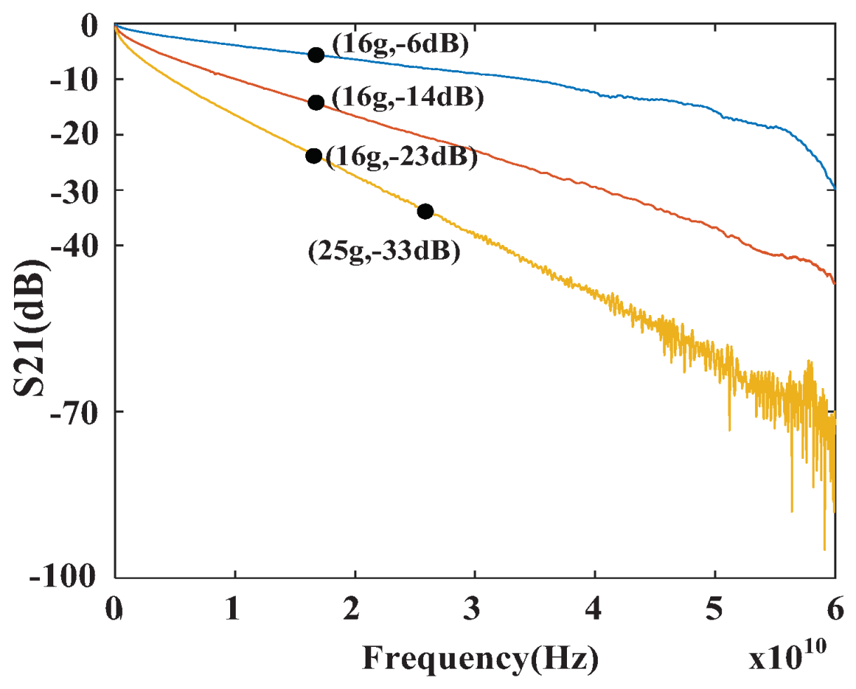
4. Simulation Results

Figure 12 shows all setups for the whole DSP verification. The verification of the design is through Simulink and Modelsim co-simulation, import the RTL code required by the design in Modelsim and compile, and then on Simulink through the oscilloscope display to observe the data. The input data of this design is generated by Maltab program, and the pseudo-random binary sequence (PRBS) generated by Matlab program is applied to the channel characterized by S21, and then the output data of Matlab is written into the txt document. Then the data of the document is sampled by simulating the sampling method of ADC in testbench file, and finally it is used as the input of the design. Figure 13 displays the adopted channel spectrums that are extracted from practical PCB traces. After the channel, the data are sampled and digitalized by an ideal ADC. These digitalized data are finally applied to the developed DSP. Figure 14 shows the equalized eye diagram before slices when operating at 100 Gb/s using a 33-dB loss channel at the Nyquist frequency (see Figure 13). It can be seen that the eye height achieves around 15.
Figure 15a,b separately give the convergence process of the FFE and DFE at 100 Gb/s with a 33-dB channel loss at the Nyquist frequency. As depicted, the FFE tap coefficients become stable within 5 us, while the DFE coefficients need 15 us to get convergence. This convergence-speed setup can effectively prevent mutual pulling between these two loops.
Table 4 summarizes the performance of the DSP in this design and compares it to other DSPs running PAM4 receivers over 56 Gb/s. Clearly, the DSP field has an area advantage compared to [10], which also uses a 28-nm process. In addition, the DSP power consumption of this design is 7.2 pJ/bit, which is higher than the DSP power consumption of [1,13], but the 7 nm FinFET process is used in the design of [1,13], compared with 28 nm is more advanced. In the design of [10], only 2-tap FFE is used, which greatly reduces the number of taps compared to this design. Therefore, the power consumption of [10] has a large advantage in the 28 nm process. In addition, the 33dB equalization capability of this design is also competitive with other designs.
Finally, we successfully realized the DSP chip applied to the Serdes receiver on the 28 nm process node. Figure 16 gives the layout of the whole system, and Figure 17 is the micrograph of the chip, where the DSP is located at the right bottom. From the simulation results and comparison with other designs, it can be concluded that the design has certain advantages on the 28 nm process node. However, it is worth noting that by optimizing the algorithm in DSP, the power consumption of the whole system can be reduced, but the balancing time will be increased. Therefore, we believe that future research can start from this and explore a method to balance power consumption and balancing ability, so as to enhance the competitiveness of this design.

5. Conclusions

A DSP for ADC-based SerDes receiver has been presented in this paper. It achieves an equalization ability of 33 dB at an operating speed of 100 Gb/s with a 1.2 mm2 area and 7.22 pJ/bit power. This design adopts the 28 nm process, it customizes a dedicated high-speed 4-to-1 MUX in the design of the DFE and adopts the speculative structure of the fixed-point operation strategy to support its high-speed operation. At the same time, an LMS algorithm based on random data selection and an average calculation based on the sigma-delta algorithm are proposed to improve the overall power efficiency of the system. Finally, by analyzing the equalization effect of different input data precisions, it is decided to determine the data precision output by ADC as 8 bits. Table 4 compares the key indexes of this design and other designs. It can be seen that for the 7nm FinFET process, due to its advanced technology, its DSP speed will have advantages. However, if more advanced technology is adopted in this design, the speed can reach more than 100 Gb/s. As for the design of the same process [10], it has advantages in power consumption due to the fewer taps applied, but the equalization ability is slightly insufficient. However, the equalization ability of this design can reach the maximum attenuation of 33 dB. In general, under the same process conditions, compared with other DSPS, the DSP designed in this paper has advantages in comprehensive area, power consumption and BERconsideration.

Author Contributions

Writing—original draft, W.L.; Writing—review and editing, M.L., X.Z., G.X., G.Y., Q.H. and Z.J. All authors have read and agreed to the published version of the manuscript.

Funding

This work was supported by the Optoelectronic and Microelectronic Devices and Integration in the National Key R&D Program of China (Grant No. 2021YFB2206602), and the National Natural Science Foundation of China (Grant No. 62074162).

Data Availability Statement

The authors declare no new data were created.

Conflicts of Interest

The authors declare no conflict of interest.

Appendix A. Parallel LMS Theory Derivation

For 16-tap 64-channel parallel structured data, the implementation of Equation (1) could be described as:
W ( 0 ) = W 1 ( 0 ) + 2 μ [ e k ( 8 ) Y ( 0 ) + e k ( 9 ) Y ( 1 ) + e k ( 56 ) Y ( 48 ) ] , W ( 1 ) = W 1 ( 1 ) + 2 μ [ e k ( 8 ) Y ( 1 ) + e k ( 9 ) Y ( 2 ) + e k ( 56 ) Y ( 49 ) ] , W ( 15 ) = W 1 ( 15 ) + 2 μ [ e k ( 8 ) Y ( 15 ) + e k ( 9 ) Y ( 16 ) + e k ( 56 ) Y ( 63 ) ] .
Here, the W 1 is the result of the previous cycle.
In the same way, the final expression of LMS DFE could be described as:
W = W 1 + 2 μ [ e k ( 1 ) Y ( 0 ) + e k ( 2 ) Y ( 1 ) + e k ( 63 ) Y ( 62 ) ]

References

  1. de Abreu Farias Neto, P.W.; Hearne, K.; Chlis, I.; Carey, D.; Casey, R.; Griffin, B.; Ngankem, F.S.F.N.; Hudner, J.; Geary, K.; Erett, M.; et al. A 112-134-Gb/s PAM4 Receiver Using a 36-Way Dual-Comparator TI-SAR ADC in 7-nm FinFET. IEEE-Solid-State Circuits Lett. 2020, 3, 138–141. [Google Scholar] [CrossRef]
  2. El-Gammal, K.A.; Hassan, A.N.; Ibrahim, S.A. A 10 Gbps ADC-Based Equalizer for Serial I/O Receiver. In Proceedings of the 2015 10th International Design & Test Symposium (IDT), Amman, Jordan, 14–16 December 2015. [Google Scholar]
  3. Upadhyaya, P.; Poon, C.F.; Lim, S.W.; Cho, J.; Roldan, A.; Zhang, W.; Namkoong, J.; Pham, T.; Xu, B.; Lin, W.; et al. A Fully Adaptive 19-58-Gb/s PAM-4 and 9.5-29-Gb/s NRZ Wireline Transceiver With Configurable ADC in 16-nm FinFET. IEEE J.-Solid-State Circuits 2019, 54, 18–28. [Google Scholar] [CrossRef]
  4. Nekouei, F.; Talebi, N.Z.; Kavian, Y.S.; Mahani, A. FPGA Implementation of LMS Self Correcting Adaptive Filter (SCAF) and Hardware Analysis. In Proceedings of the 2012 8th International Symposium on Communication Systems, Networks & Digital Signal Processing (CSNDSP), Poznan, Poland, 18–20 July 2012. [Google Scholar]
  5. Trakultritrung, A.; Thanangchusin, E.; Chivapreecha, S. Distributed Arithmetic LMS Adaptive Filter Implementation without Look-Up Table. In Proceedings of the 2012 9th International Conference on Electrical Engineering/Electronics, Computer, Telecommunications and Information Technology, Phetchaburi, Thailand, 16–18 May 2012. [Google Scholar]
  6. Kiran, S.; Cai, S.; Zhu, Y.; Hoyos, S.; Palermo, S. Digital Equalization With ADC-Based Receivers. IEEE Microw. Mag. 2019, 50, 62–79. [Google Scholar] [CrossRef]
  7. Lin, C.; Wu, A. Soft-Threshold-Based Multilayer Decision Feedback Equalizer (STM-DFE) Algorithm and VLSI Architecture. IEEE Trans. Signal Process. 2005, 53, 3325–3336. [Google Scholar]
  8. Upadhyaya, P.; Poon, C.F.; Lim, S.W.; Cho, J.; Roldan, A.; Zhang, W.; Pham, J.N.T.; Pham, T.; Pham, T. A Fully Adaptive 19-to-56Gb/s PAM-4 Wireline Transceiver with a Configurable ADC in 16nm FinFET. In Proceedings of the 2018 IEEE International Solid-State Circuits Conference—(ISSCC), San Francisco, CA, USA, 11–15 February 2018. [Google Scholar]
  9. Roshan-Zamir, A.; Iwai, T.; Fan, Y.H.; Kumar, A.; Yang, H.W.; Sledjeski, L.; Palermo, S. A 56-Gb/s PAM4 Receiver With Low-Overhead Techniques for Threshold and Edge-Based DFE FIR- and IIR-Tap Adaptation in 65-nm CMOS. IEEE J.-Solid-State Circuits 2019, 54, 672–684. [Google Scholar] [CrossRef]
  10. Li, H.; Hsu, C.-M.; Sharma, J.; Jaussi, J.; Balamurugan, G. A 100 Gb/s-8.3dBm-Sensitivity PAM-4 Optical Receiver with Integrated TIA, FFE and Direct-Feedback DFE in 28 nm CMOS. IEEE J.-Solid-State Circuits 2021, 57, 44–53. [Google Scholar] [CrossRef]
  11. Guo, S.; Ding, L.; Jin, J. A 16/32GB/s NRZ/PAM4 Receiver with Dual-Loop CDR and Threshold Voltage Calibration. In Proceedings of the 2019 IEEE 13th International Conference on ASIC (ASICON), Chongqing, China, 29 October–1 November 2019. [Google Scholar]
  12. IEEE Std 802.3; IEEE Standard for Ethernet. IEEE: New York, NY, USA, 2018.
  13. Xu, D.; Kou, Y.; Lai, P.; Cheng, Z.; Cheung, T.Y.; Moser, L.; Liu, X.; Zhang, Y.; Lam, M.P.; Jia, H.; et al. A Scalable Adaptive ADC/DSP-Based 1.25-to-56 Gbps/112 Gbps High-Speed Transceiver Architecture Using Decision-Directed MMSE CDR in 16 nm and 7 nm. In Proceedings of the 2021 IEEE International Solid-State Circuits Conference (ISSCC), San Francisco, CA, USA, 13–22 February 2021. [Google Scholar]
Figure 1. DSP main channel.
Electronics 12 00257 g001
Figure 2. Implementation of the 1-tap speculative DFE.
Electronics 12 00257 g002
Figure 3. The timing diagram of DFE MUX.
Electronics 12 00257 g003
Figure 4. Custom 4 to 1 MUX.
Electronics 12 00257 g004
Figure 5. 16-tap parallel FFE structure.
Electronics 12 00257 g005
Figure 6. The effect of truncating in FFE and ideal results of MATLAB. (a) 9 bits. (b) MATLAB results. (c) 8 bits. (d) 10 bits.
Electronics 12 00257 g006
Figure 7. LMS adaptation for the FFE. (a) Traditional implementation utilizing all parallel data averaging. (b) Proposed implementation using randomly-selected data averaging.
Electronics 12 00257 g007
Figure 8. LMS adaptation for the DFE. (a) Traditional implementation utilizing all parallel data. (b) Proposed implementation using randomly-selected data.
Electronics 12 00257 g008
Figure 9. Averages. (a) Moving average filter. (b) 1st-order sigma delta integrator.
Electronics 12 00257 g009
Figure 10. The equalization effect for different data digitalization bits in a −14 dB channel loss at 64 Gb/s. (a) 5 bits. (b) 6 bits. (c) 7 bits. (d) 8 bits.
Electronics 12 00257 g010
Figure 11. Trend of vertical eye closure and vertical eye-opening ratio with attenuation. (a) VEC. (b) VEOR.
Electronics 12 00257 g011
Figure 12. The verification structure.
Electronics 12 00257 g012
Figure 13. The S21 for channels.
Electronics 12 00257 g013
Figure 14. The eye diagram in 100 Gb/s −33dB.
Electronics 12 00257 g014
Figure 15. LMS FFE/DFE coefficients in 100 Gb/s −33 dB. (a) FFE coefficients. (b) DFE coefficient.
Electronics 12 00257 g015
Figure 16. The layout of the whole system.
Electronics 12 00257 g016
Figure 17. The micrograph of the chip.
Electronics 12 00257 g017
Table 1. The VEC and VEOR for different FFE coefficients width.
Width8910
VEC5.014.844.69
VEOR6.937.387.57
Table 2. The resource comparison in LMS DFE.
TypeSum FactorSum PipelineTechnologyClock (Hz)No.AddersPower
Full63328 nm1 G12,67620.5 mW
Random1128 nm1 G12902.0 mW
Table 3. 4th-order moving average filter versus 1st-order sigma-delta.
TypeOrderTechnologyChannelClock (Hz)No.AddersPower
Moving average428 nm641 G36,14043 mW
Sigma-delta128 nm641 G10,40714 mW
Table 4. PAM4 receiver performance comparisons.
ReferencesThis Work[10][13][1]
Technology28 nm CMOS28 nm CMOS7 nm FinFET7 nm FinFET
Data rate100 Gb/s100 Gb/s112 Gb/s134 Gb/s
Data formatePAM4PAM4PAM4PAM4
Equalization16-tap FFE,1-tap DFE2-tap FFE,2-tap DFE32-tap FFE,1-tap DFECTLE,16-tap FFE,1-tap DFE
Channel33 dB-35 dB33 dB
Area1.2 mm25.5 mm2-0.383 mm2
Supply0.9 V-0.75 V/0.9 V/1.2 V0.88 V/1.2 V/1.5 V
DSP power efficiency7.22 pJ/bit3.9 pJ/bit3.0 pJ/bit5.1 pJ/bit
BER 1 × 10 8 - 1 × 10 9 1 × 10 6
Disclaimer/Publisher’s Note: The statements, opinions and data contained in all publications are solely those of the individual author(s) and contributor(s) and not of MDPI and/or the editor(s). MDPI and/or the editor(s) disclaim responsibility for any injury to people or property resulting from any ideas, methods, instructions or products referred to in the content.

