


A Wirelessly-Powered Body-Coupled Data Transmission with Multi-Stage and Multi-Source Rectifier


Abstract
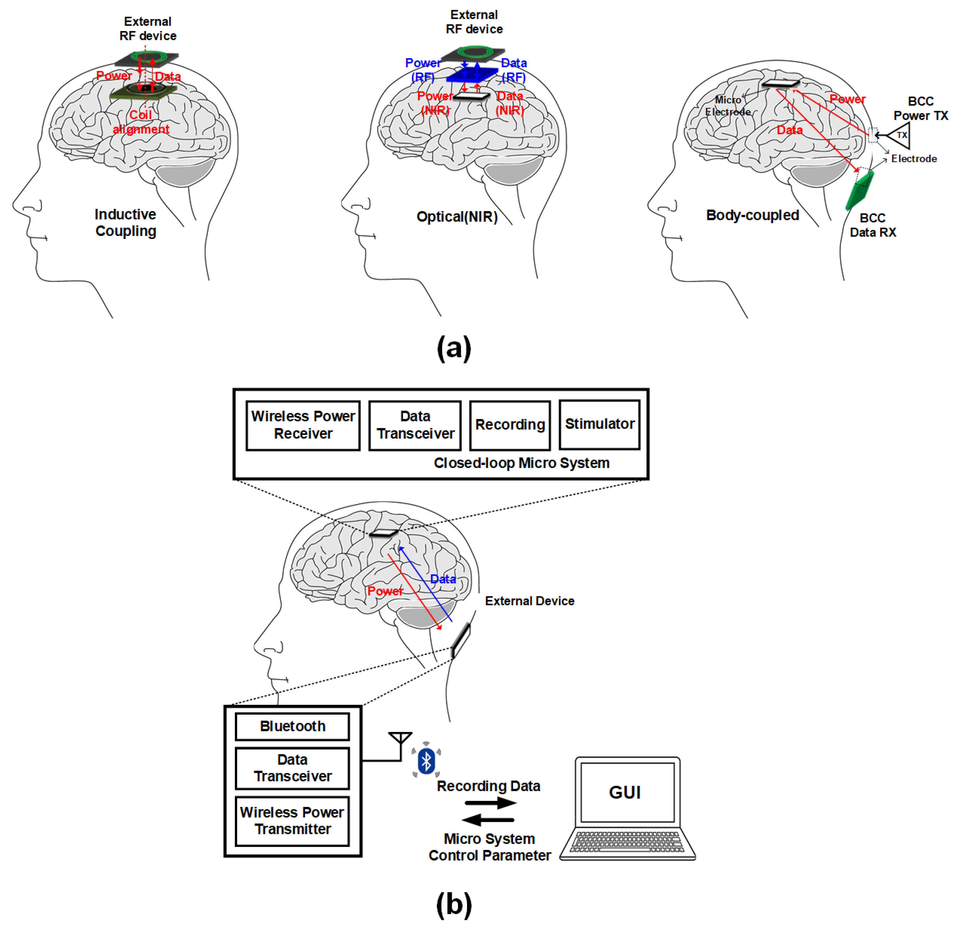
:1. Introduction
2. Channel Characteristics and Safety Considerations of BC Transmission
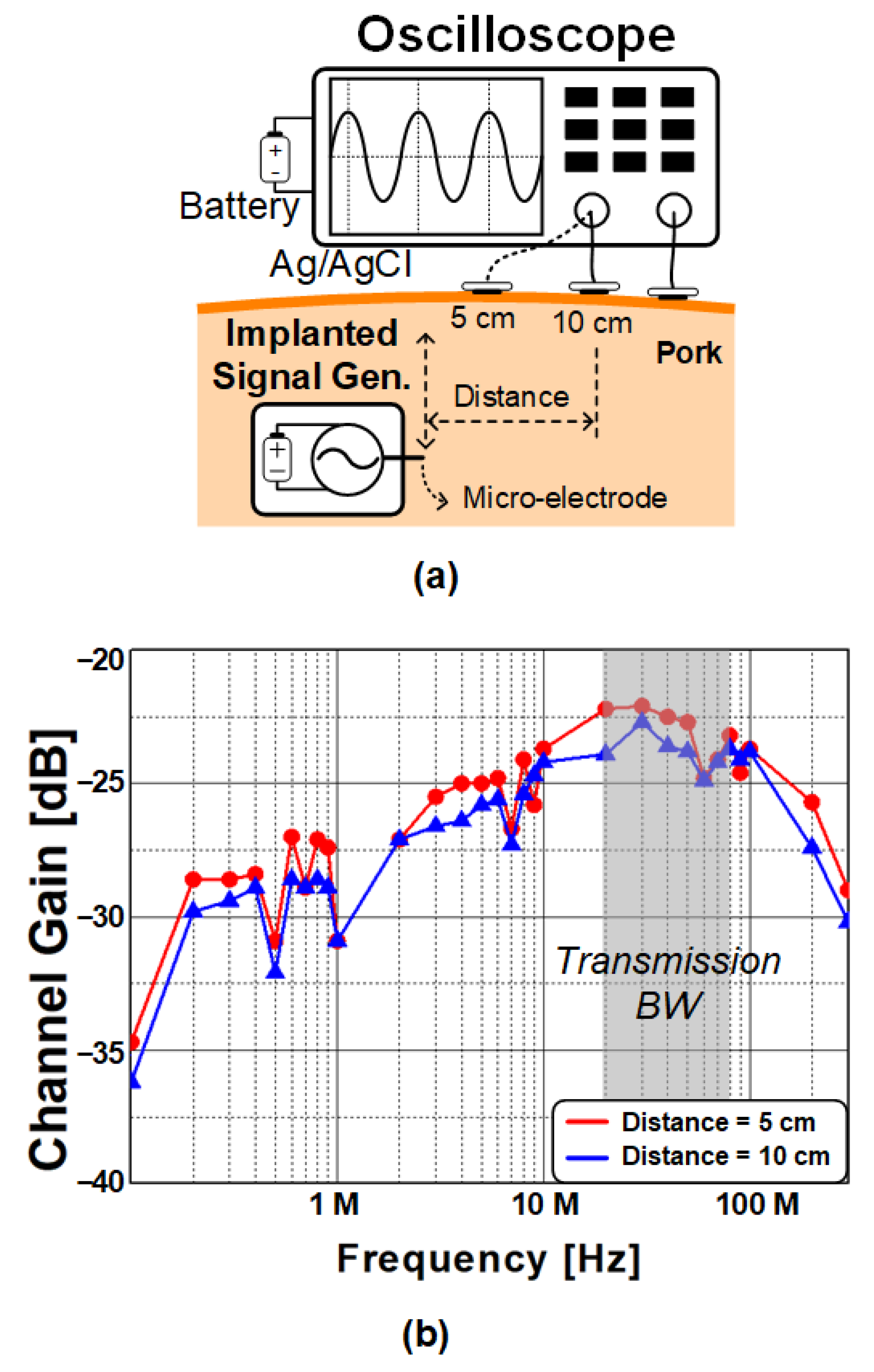
2.1. Characteristics of Body-Coupled Channel
2.2. Safety Considerations for BC Transmission
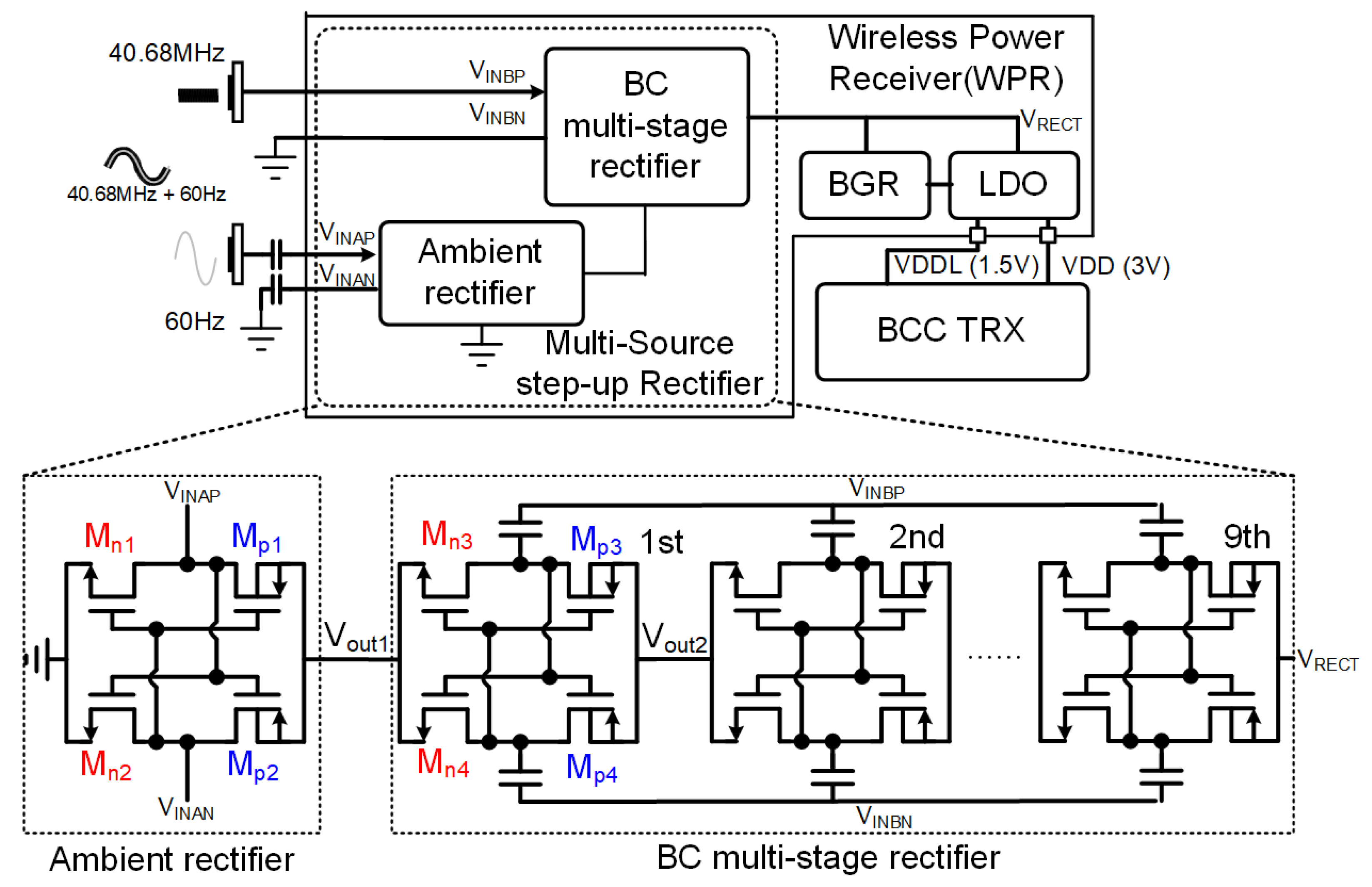
3. System Implementation
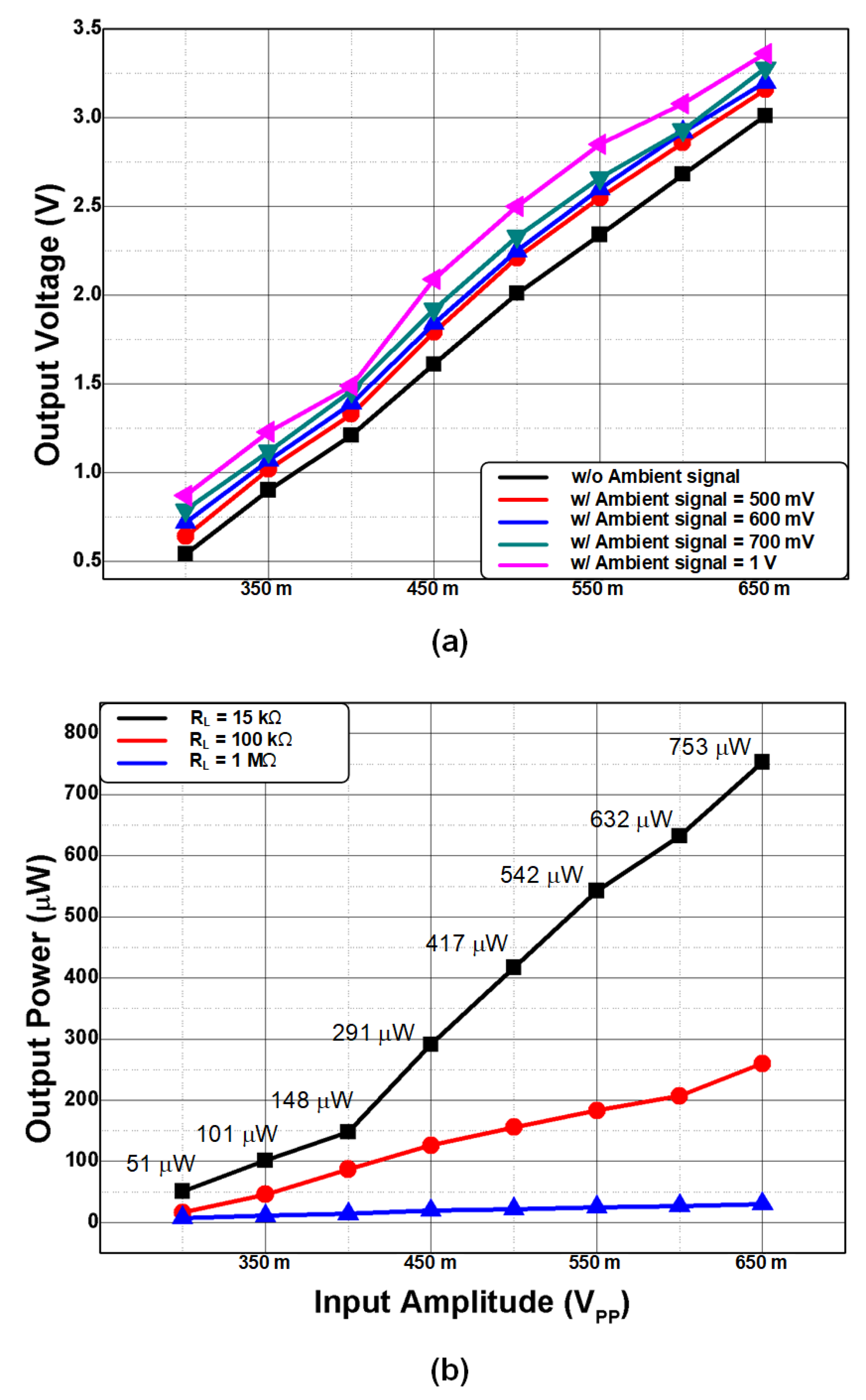
3.1. Wireless Power Receiver
3.2. Body-Coupled (BC) Transmitter
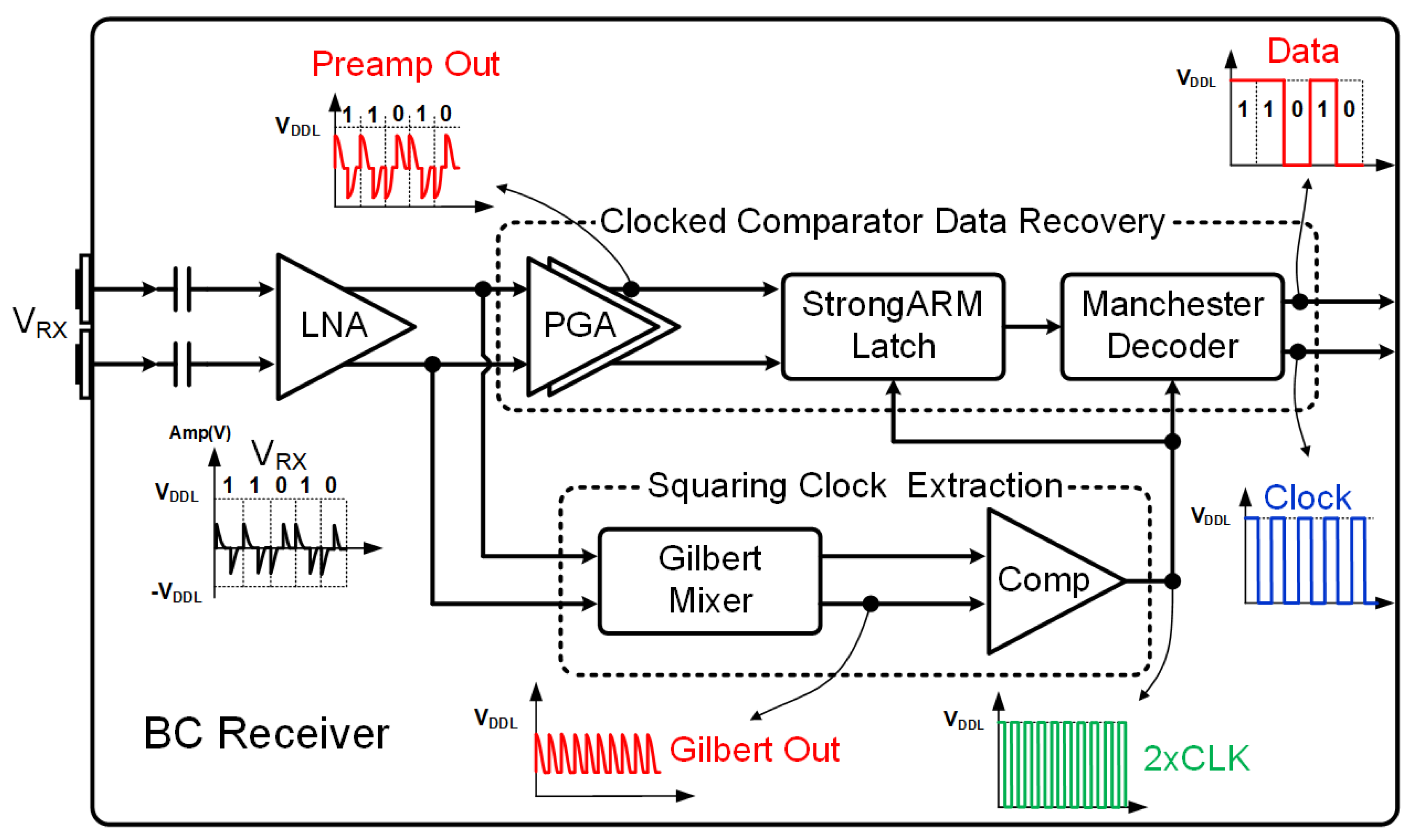
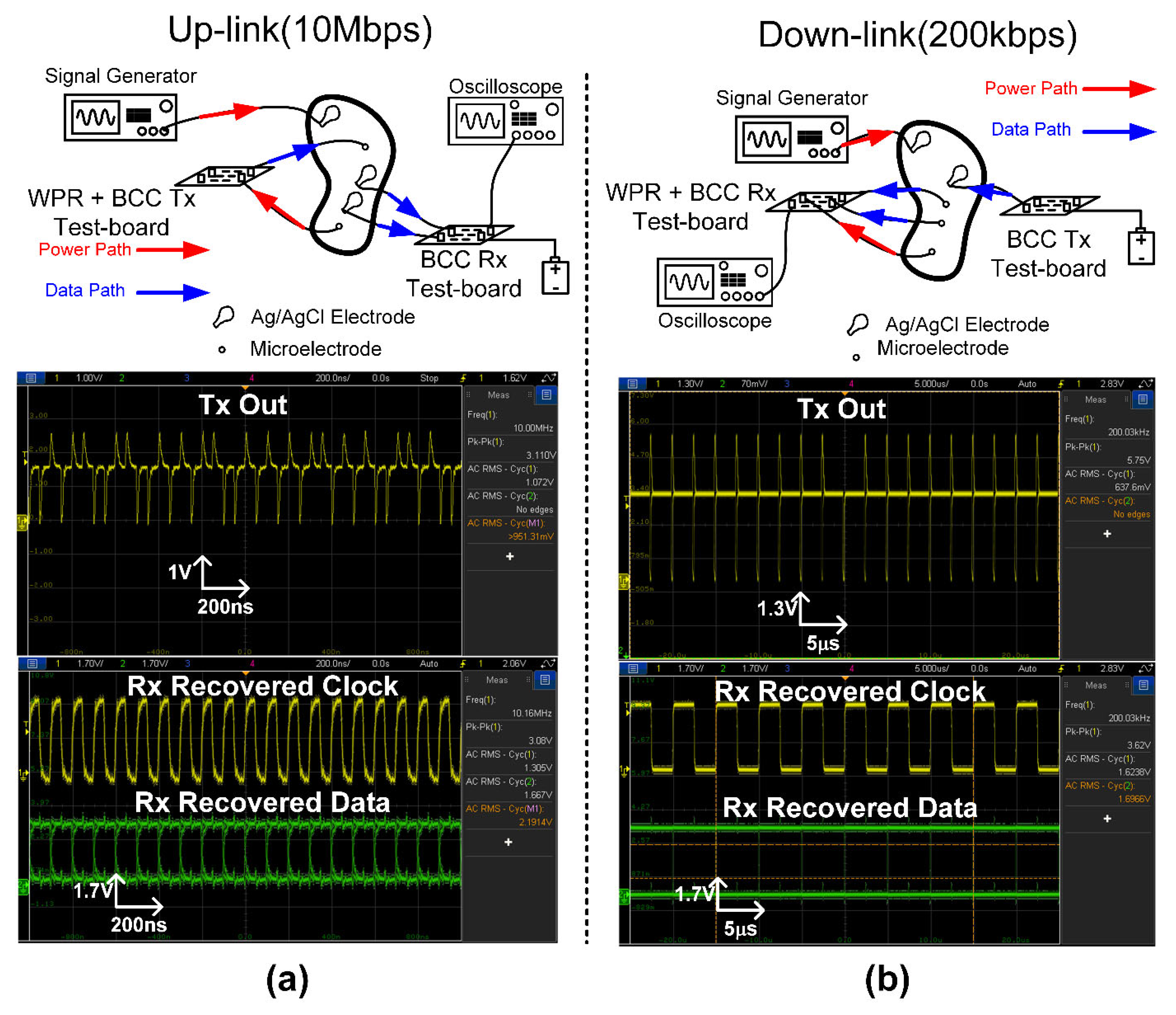
3.3. BC Receiver
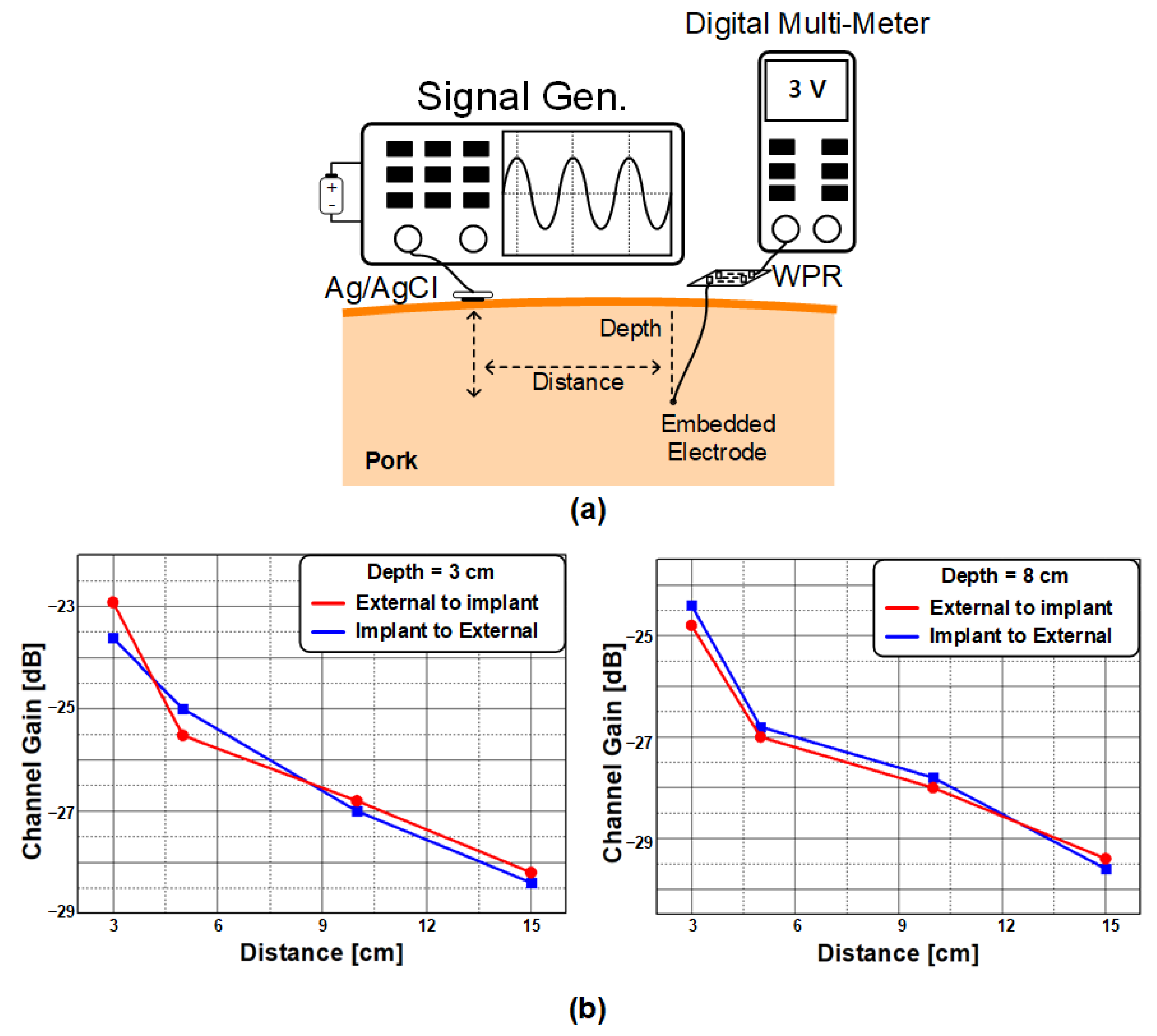
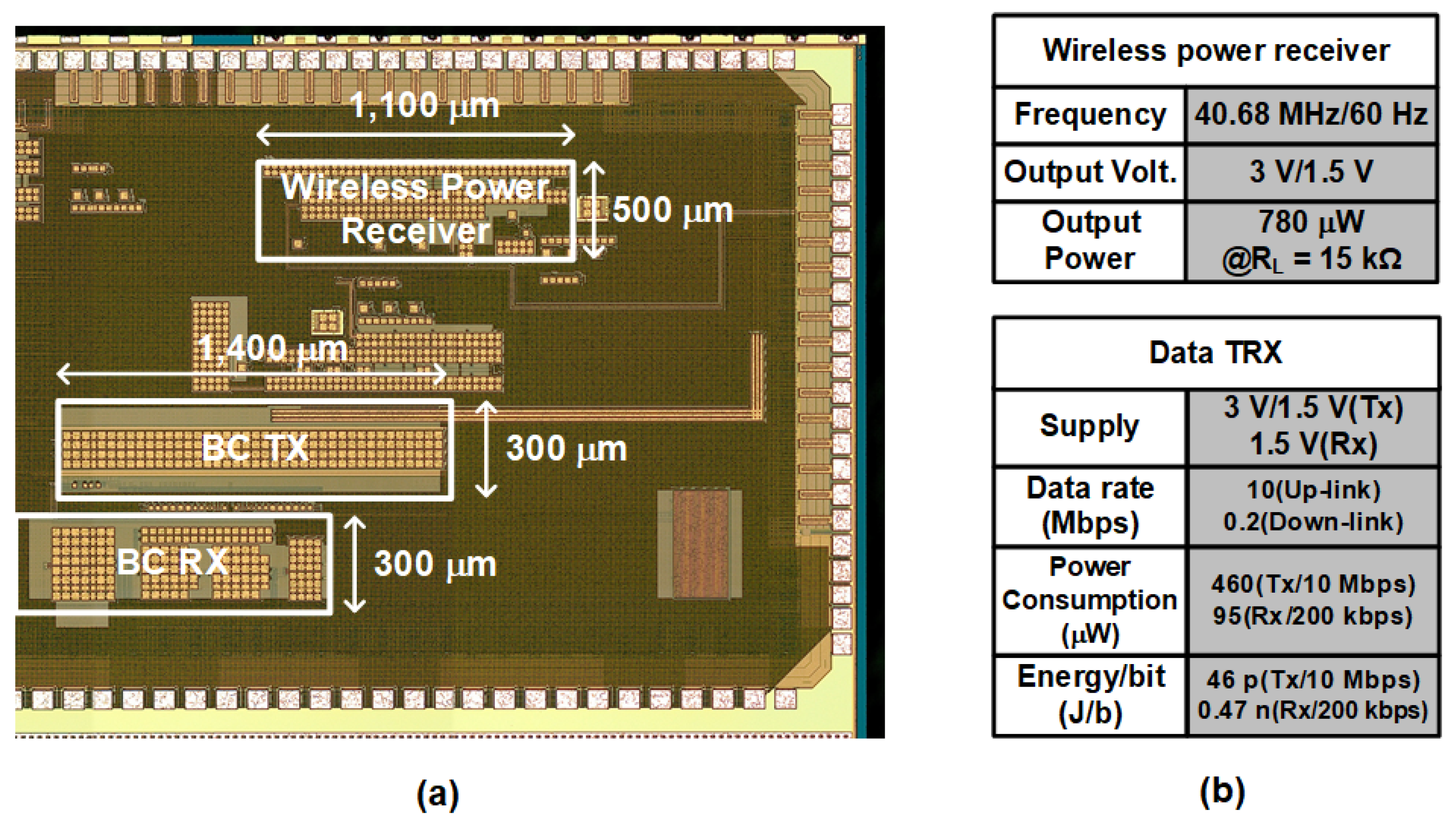
4. Measurement Results
5. Conclusions
Author Contributions
Funding
Data Availability Statement
Conflicts of Interest
References
- Maharbiz, M.M.; Muller, R.; Alon, E.; Rabaey, J.M.; Carmena, J.M. Reliable next-generation cortical interfaces for chronic brain–machine interfaces and neuroscience. Proc. IEEE 2017, 105, 73–82. [Google Scholar] [CrossRef]
- Muller, R.; Ghanbari, M.M.; Zhou, A. Miniaturized wireless neural interfaces: A tutorial. IEEE Solid State Circuits Mag. 2021, 13, 88–97. [Google Scholar] [CrossRef]
- Lee, J.; Rhew, H.-G.; Kipke, D.R.; Flynn, M.P. A 64 channel programmable closed-loop neurostimulator with 8 channel neural amplifier and logarithmic ADC. IEEE J. Solid State Circuits 2010, 45, 1935–1945. [Google Scholar] [CrossRef]
- Lopez, C.M.; Andrei, A.; Mitra, S.; Welkenhuysen, M.; Eberle, W.; Bartic, C.; Puers, R.; Yazicioglu, R.F.; Gielen, G.G.E. An implantable 455-active-electrode 52-channel CMOS neural probe. IEEE J. Solid State Circuits 2014, 49, 248–261. [Google Scholar] [CrossRef]
- Van Daal, R.J.J.; Aydin, Ç.; Michon, F.; Aarts, A.A.A.; Kraft, M.; Kloosterman, F.; Haesler, S. Implantation of neuropixels probes for chronic recording of neuronal activity in freely behaving mice and rats. Nat. Protoc. 2021, 16, 3322–3347. [Google Scholar] [CrossRef] [PubMed]
- Jia, Y.; Guler, U.; Lai, Y.; Gong, Y.; Weber, A.; Li, W.; Ghovanloo, M. A trimodal wireless implantable neural interface system-on-chip. IEEE Trans. Biomed. Circuits Syst. 2020, 14, 1207–1217. [Google Scholar] [CrossRef] [PubMed]
- El Ansary, M.; Xu, J.; Filho, J.S.; Dutta, G.; Long, L.; Tejeiro, C.; Shoukry, A.; Tang, C.; Kilinc, E.; Joshi, J.; et al. Bidirectional peripheral nerve interface with 64 second-order opamp-less ΔΣ ADCs and fully integrated wireless power/data transmission. IEEE J. Solid State Circuits 2021, 56, 3247–3262. [Google Scholar] [CrossRef]
- Xia, L.; Cheng, J.; Glover, N.E.; Chiang, P. 0.56 V, −20 dBm RF-Powered, Multi-Node Wireless Body Area Network System-on-a-Chip with Harvesting-Efficiency Tracking Loop. IEEE J. Solid State Circuits 2014, 49, 1345–1355. [Google Scholar] [CrossRef]
- Li, W.; Duan, Y.; Rabaey, J.M. A 200 Mb/s inductively coupled wireless transcranial transceiver achieving 5e-11 BER and 1.5 pJ/b transmit energy efficiency. In Proceedings of the 2018 IEEE International Solid-State Circuits Conference (ISSCC), Digital Technology Papers, San Francisco, CA, USA, 11–15 February 2018; pp. 290–292. [Google Scholar]
- Ghanbari, M.M.; Piech, D.K.; Shen, K.; Alamouti, S.F.; Yalcin, C.; Johnson, B.C.; Carmena, J.M.; Maharbiz, M.M.; Müller, R. 17.5 A 0.8 mm3 Ultrasonic Implantable Wireless Neural Recording System with Linear AM Backscattering. In Proceedings of the 2019 IEEE International Solid-State Circuits Conference (ISSCC), San Francisco, CA, USA, 17–21 February 2019; pp. 284–286. [Google Scholar]
- Lee, S.; Cortese, A.J.; Trexel, P.; Agger, E.R.; McEuen, P.L.; Molnar, A.C. A 330 μm × 90 μm opto-electronically integrated wireless system-on-chip for recording of neural activities. In Proceedings of the 2018 IEEE International Solid-State Circuits Conference (ISSCC), San Francisco, CA, USA, 11–15 February 2018; pp. 292–294. [Google Scholar]
- Lee, C.; Kim, B.; Kim, J.; Lee, S.; Jeon, T.; Choi, W.; Yang, S.; Ahn, J.; Bae, J.; Chae, Y. A Miniaturized Wireless Neural Implant with Body-Coupled Power Delivery and Data Transmission. IEEE J. Solid State Circuits 2022, 57, 3212–3227. [Google Scholar] [CrossRef]
- Yuk, B.; Kim, B.; Park, S.; Huh, Y.; Bae, J. An Implantable Body Channel Communication System with 3.7-pJ/b Reception and 34-pJ/b Transmission Efficiencies. IEEE Solid-State Circuits Lett. 2020, 3, 50–53. [Google Scholar] [CrossRef]
- Kim, B.; Yuk, B.; Bae, J. A Wirelessly-Powered 10 Mbps 46-pJ/b Body Channel Communication System with 45% PCE Multi-Stage and Multi-Source Rectifier for Neural Interface Applications. In Proceedings of the 2021 IEEE Asian Solid-State Circuits Conference (A-SSCC), Busan, Republic of Korea, 7–10 November 2021; pp. 1–3. [Google Scholar]
- Li, J.; Dong, Y.; Park, J.; Lin, L.; Tang, T.; Yoo, J. Body-Area Powering with Human Body-Coupled Power Transmission and Energy Harvesting ICs. IEEE Trans. Biomed. Circuits Syst. 2020, 14, 1263–1273. [Google Scholar] [CrossRef] [PubMed]
- Huang, H.; Zhang, M.; Li, G.; Wang, Z. A 2Mbps sub-100 µW Crystal-less RF Transmitter with Energy Harvesting for Multi-Channel Neural Signal Acquisition. In Proceedings of the 2019 IEEE Asian Solid-State Circuits Conference (A-SSCC), Macau, China, 4–6 November 2019; pp. 157–160. [Google Scholar]
- Chang, T.C.; Wang, M.L.; Charthad, J.; Weber, M.J.; Arbabian, A. 27.7 A 30.5 mm3 fully packaged implantable device with duplex ultrasonic data and power links achieving 95kb/s with <10−4 BER at 8.5 cm depth. In Proceedings of the 2017 IEEE International Solid-State Circuits Conference (ISSCC), San Francisco, CA, USA, 5–9 February 2017; pp. 460–461. [Google Scholar]


| ASSCC [16] | ISSCC [17] | TBioCAS [6] | TBioCAS [15] | This Work | |
|---|---|---|---|---|---|
| Wireless Power Receiver | |||||
| Technology | 180 nm CMOS | 65 nm CMOS | 0.35 μm CMOS | 40 nm CMOS | 180 nm CMOS |
| Power link | Inductive | Ultra-sound | Inductive | Body-coupled | Body-coupled |
| Rectifier Topology | Active-rectifier | Active-rectifier | Voltage-doubler | Cross-coupled | Cross-coupled |
| Frequency | 6.78 MHz | 0.95 MHz | 13.56 MHz | 40 MHz/60 Hz | 40.68 MHz/60 Hz |
| Output volt. (V) | 1/0.6/0.3 | 1 | 4/3.3/1.8 | N.A. | 3/1.5 |
| Output power (μW) | N.A. | N.A. | N.A. | 102.5 | 780 |
| Data TRX | |||||
| Supply (V) | 1/0.3 | 1 | N.A. | 3/1.5 | |
| Data link | RF | Ultra-sound | RF/Inductive | Body-coupled | |
| Modulation | OOK | OOK | OOK | Direct digital | |
| Data rate (Mbps) | 2 | 0.1/0.025 | 6.78/0.05 | 10/0.2 | |
| Power consumption (μW) | 96 | 177 | N.A. | 460/95 | |
| Energy/bit (J/b) | 48 p | 1.77 n | 46 p/470 p | ||
Disclaimer/Publisher’s Note: The statements, opinions and data contained in all publications are solely those of the individual author(s) and contributor(s) and not of MDPI and/or the editor(s). MDPI and/or the editor(s) disclaim responsibility for any injury to people or property resulting from any ideas, methods, instructions or products referred to in the content. |
© 2023 by the authors. Licensee MDPI, Basel, Switzerland. This article is an open access article distributed under the terms and conditions of the Creative Commons Attribution (CC BY) license (https://creativecommons.org/licenses/by/4.0/).
Share and Cite
Kim, B.; Bae, J. A Wirelessly-Powered Body-Coupled Data Transmission with Multi-Stage and Multi-Source Rectifier. Electronics 2023, 12, 2181. https://doi.org/10.3390/electronics12102181
Kim B, Bae J. A Wirelessly-Powered Body-Coupled Data Transmission with Multi-Stage and Multi-Source Rectifier. Electronics. 2023; 12(10):2181. https://doi.org/10.3390/electronics12102181
Chicago/Turabian StyleKim, Byeongseol, and Joonsung Bae. 2023. "A Wirelessly-Powered Body-Coupled Data Transmission with Multi-Stage and Multi-Source Rectifier" Electronics 12, no. 10: 2181. https://doi.org/10.3390/electronics12102181
APA StyleKim, B., & Bae, J. (2023). A Wirelessly-Powered Body-Coupled Data Transmission with Multi-Stage and Multi-Source Rectifier. Electronics, 12(10), 2181. https://doi.org/10.3390/electronics12102181