Article

Hardware and Software Implementation of the Embedded Controlling System for the TuMag Camera

by
Manuel Rodríguez Valido
1,*,
David Orozco Suárez
2,
David Hernández Exposito
3,
Eduardo Magdaleno Castelló
1 and
Basilio Ruiz Cobo
3
1
Department of Industrial Engineering, University of La Laguna, 38203 San Cristóbal de La Laguna, Spain
2
Institute of Astrofísica de Andalucía, Consejo Superior de Investigaciones Científicas, 18080 Granada, Spain
3
Institute of Astrophysics of Canary Islands, 38205 San Cristóbal de La Laguna, Spain
*
Author to whom correspondence should be addressed.
Electronics 2023, 12(19), 4071; https://doi.org/10.3390/electronics12194071
Submission received: 18 July 2023 / Revised: 25 September 2023 / Accepted: 25 September 2023 / Published: 28 September 2023

Abstract

:
The main objective of this paper is to present the design and implementation of an embedded controlling system for the Tunable Magnetograph (TuMag) instrument camera sensor and test-bench software application for camera laboratory characterization. The TuMag camera is based on a new scientific sensor GPIXEL SENSE400 device family equipped with an FPGA. The camera sensor has an active area of 2048 × 2048 pixels and reaches a frame rate of up to 48 frames per second. The embedded controlling system was implemented on an Artix 7 FPGA, which oversees controlling the image sensor through a configuration interface. It controls the read-out of the sensor data and the communication of commands with the host device. The camera has a standard CoaXPress communication interface of up to 3125 Gbps. The FPGA embedded control system allows bit, word, and serial channel calibration and the modification of several parameters, such as the region of interest (RoI) size, exposition time, hardware or software trigger, single or continuous acquisition modes, sensor gain, and adjustment of the black level offset and exposition time. In addition, the firmware has a temperature controller, voltage level monitoring, and an enable–disable power sensor. In addition, the test-bench software application is a library developed in Python 3.7. It is a wrapper for the standard GeniCan commercial frame grabber interpreter. This wrapper permits the improvement of the interaction and interface between the user and the hardware in the camera calibration. The test-bench software application permits the reduction of costs and the transport risk of the TuMag camera between different laboratories. All TuMag embedded control systems and test-bench software application functionalities were successfully tested according to scientific requirements.

1. Introduction

The Sunrise III balloon-borne solar mission [1], led by the Max Planck Institute for Solar System Research (MPS; Germany) and with partners from the USA, Japan, Spain, and Germany, is the third solar observatory dedicated to the investigation of key processes governing the physics of magnetic fields and convective plasma flows in the lower solar atmosphere. These processes are crucial for our understanding of the magnetic activity of the Sun and the outwards transport of energy to heat its outer atmosphere and to fuel eruptions and coronal mass ejections, phenomena that affect the Earth’s environment. Designed for operation in the stratosphere (at heights of approximately 37 km) to avoid image degradation due to turbulence in the lower terrestrial atmosphere, Sunrise III carries three scientific instruments: the UV Spectropolarimeter and Imager (SUSI) instrument, a grating-based spectropolarimeter that will explore the rich near-UV range between 300 nm and 410 nm [2]; the Chromospheric Infrared spectroPolarimeter (SCIP), which allows the combined measurement of photospheric and chromospheric layers using spectral lines formed in the infrared [3]; and the Tunable Magnetograph (TuMag), a visible imaging spectropolarimeter able to observe the solar photosphere and the lower chromosphere [4], which was fully developed and built by the Spanish Space Solar Physics Consortium (S3PC) (S3PC partners are IAA-CSIC, IAC (Instituto de Astrofísica de Canarias), IDR/UPM (Instituto de Microgravedad “Ignacio Da Riva”, Universidad Politécnica de Madrid), INTA (Instituto Nacional de Técnica Aeroespacial), and UV (Universidad de Valencia)) led by the Instituto de Astrofísica de Andalucía (IAA-CSIC, Spain).
The design and development of a novel instrumentation for stratospheric flights is a technological challenge due to the near-vacuum conditions prevailing at those heights. In the case of SCIP and TuMag instruments, scientific cameras are one of the most critical subsystems. Indeed, none of the available cameras in the market met the scientific requirements of the instruments in terms of photon budget, speed, and flight compatibility. Hence, the S3PC designed and developed new cameras from scratch [5], except for the sensor, which was purchased on the market. In particular, the TuMag camera is based on the scientific sensor GPIXEL SENSE400-BSI [6,7,8], a rolling shutter, backside illuminated sensor with an active area of 2048 × 2048 pixels that reaches a frame rate of up to 48 frames per second in standard mode (STD).
The main objective of this paper is to present the design and implementation of an Embedded Controlling System for the TuMag camera sensor (TuMag-ECS) and a Test Bench Software Library, TBSL, to manage thermal characterization in the laboratory. The main task of the TuMag-ECS is to manage the 3125 Mbps CoaXPress Communication interface between the sensor and the host as well as to control any other IP or custom module to run and configure the camera and monitor the housekeeping of the device. The TBSL, on the other hand, is a useful tool for optical and thermal characterization tests of the instrument under vacuum conditions. That is, before the flight, rigorous and demanding processes will be carried out to validate the performance of the TuMag camera in near-vacuum conditions. Consequently, the TuMag instrument, including the camera and the host (the full optical and electronics units), must be transported to each center to mount different experimental setups. The transport of this equipment involves risks to its integrity and requires human and economic project resources to execute the necessary logistics. For these reasons, we have developed the TSBL, which is based on a commercial CoaXPress frame grabber, to be able to test the TuMag camera in different laboratories of the consortium of the research group without the need to carry the whole instrument.
The design presented in this work represents a challenge and an advancement in terms of scientific and technical knowledge. The TuMag-ECS design allows us to investigate the behavior of different technologies and methods, such as the Gpixel CMOS detector, the Artix 7 FPGA, and the CoaXPress interface, in a harsh environment.
The rest of the paper is organized as follows: Section 2, Materials and Methods, describes the general FPGA block architecture of the TuMag camera. This section details the TuMag-ECS architecture and its main hardware blocks and functionalities, as well as the embedded software that controls the communications between the camera–host and the test bench software application to set up laboratory experiments. Finally, Section 3 presents the results and conclusions.

2. Materials and Methods

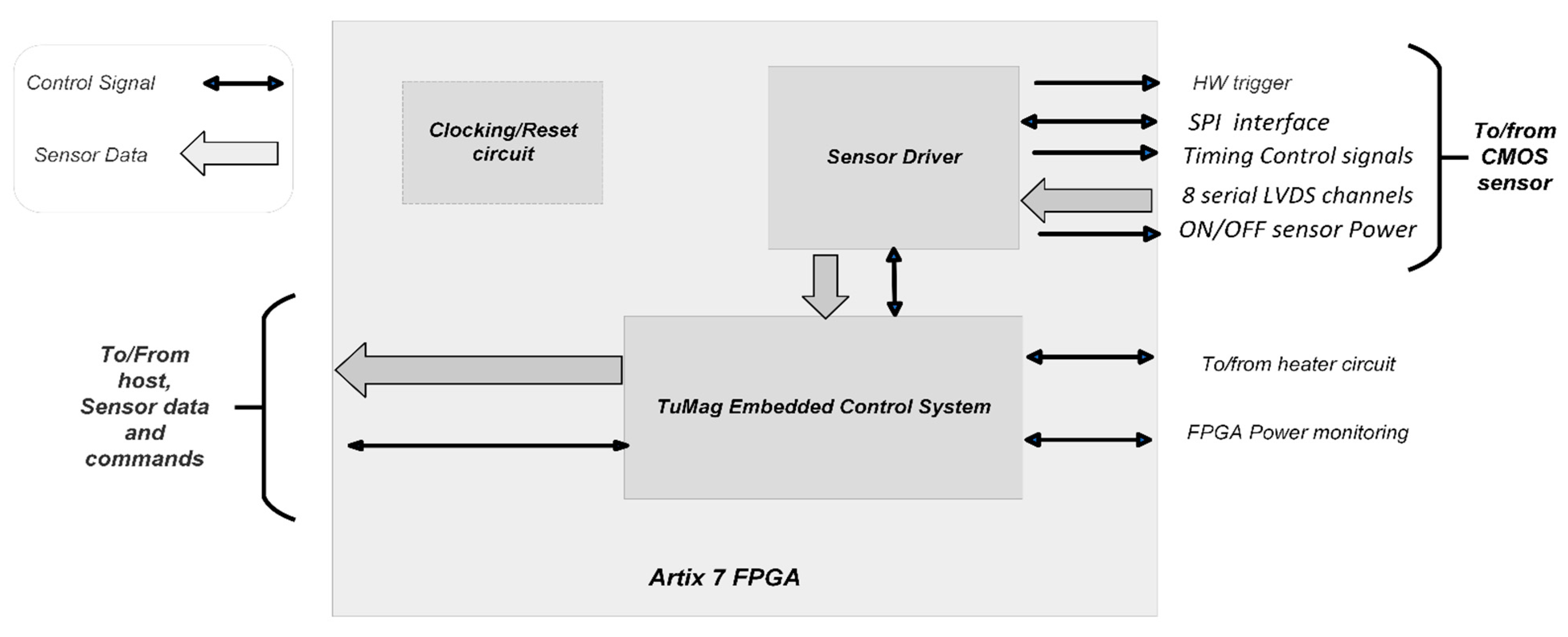
The architecture of the TuMag camera FPGA blocks diagram is shown in Figure 1. It consists of two main blocks: the sensor driver module and the TuMag embedded control system module. The sensor driver module is responsible for direct communication with the CMOS detector. It defines an SPI interface to access the internal registers of the sensor, a finite state machine circuit that generates 19 timing control signals to read the sensor data synchronously, and a circuit to read and convert 8 serial LVDS 12-bit data channels to 12 parallel words. In addition, the sensor driver has implemented a hardware circuit to calibrate the sensor, channel order, readout electronic control, etc. The TuMag Embedded Control System (TuMag-ECS) module is a core-based MicroBlaze soft processor that manages the 3125 Gbps CoaXPress communication interface [9] between the host (or frame grabber) and the sensor. It also serves as a communication interface between the heater and the temperature controller sensor, monitors the supply 24 V voltage of the TuMag camera, and switches the sensor on/off. Additionally, the TuMag-ECS, through the AXI-Lite and AXI4 video stream buses, sets and manages the communications of the sensor driver to configure the sensor and/or read the data. The TuMag camera firmware was implemented in an Artix 7 FPGA using VHDL and Verilog hardware description language. The Artix 7 FPGA device provides the highest performance-per-watt fabric, transceiver line rates, and DSP processing in a cost-optimized FPGA [10].
In addition, TuMag-ECS is in charge of bit, word, and serial channel calibration and of the modification of several parameters, such as the region of interest (ROI) size, exposure time, hardware or software trigger, single or continuous acquisition modes, sensor gain, and adjustment of the black level offset.
The sensor GSENSE400BSI is a scientific [6,7,8], back-illuminated CMOS image sensor with a wide dynamic range of pixels produced by Gpixel INC. The sensor has the advantages of high sensitivity, low noise, and high integration, including a 12-bit ADC, a temperature sensor, a PLL, and an SPI controller on-chip. The ADC is used to convert analog signals into 12-bit digital signals, and the PLL is used for on-chip clock management. The SPI controller is used for on-chip register configuration, which can change the on-chip PGA gain, data readout direction, PLL crossover multiplier, and operating mode. In addition, the CMOS sensor has two modes of operation: standard (STD) mode and high dynamic range (HDR) mode. Table 1 lists the key specifications of GSENSE400BSI.

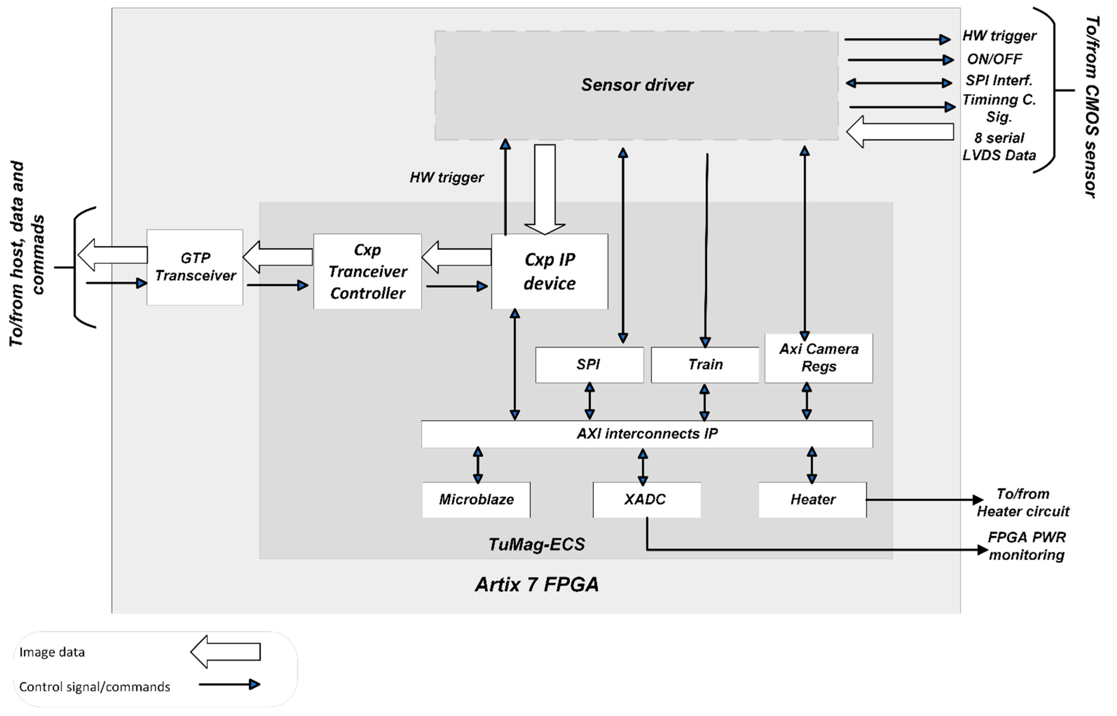
2.1. TuMag-ECS Architecture

The TuMag-ECS was implemented with the Vivado tool (Figure 2); in the Supplementary Material, we added a PDF file with the block diagram of all TuMag-ECS circuits. The main task of this system is to control both the GSENSE400BSI sensor driver (right side) and the CoaXPress communication interface with the host or frame grabber (left side). In addition, it also controls/monitors other modules (IP) necessary for the instrument, such as the heater module (temperature controller), the SPI module to read the internal sensor registers, the train module to put the sensor in training mode, the AXI_to Camera register necessary to configure the sensor, the XADC module to monitor internal FPGA parameters, and, finally, the Easii_cxp_dev controller of the CoaXPress communication interface.
This embedded system is based on an architecture defined by an AXI4-Lite bus, which, by means of the software drivers of each module, allows carrying out the necessary reading and writing operations for the following tasks: monitoring the heater status, monitoring the supply voltage of the system, configuring the operating modes of the sensor, and managing all other functionalities defined in the firmware of TuMag ECS. These drivers are implemented through simple software functions executed on a MicroBlaze soft-processor IP core (2017.1) provided by Xilinx. In this processor, the software control application controls/decodes the communications between the sensor and the host and vice versa. Additionally, it manages all IPs belonging to the architecture of the embedded control system. These IP cores are the heater control, spi, AXI_to_camerareg, sensor train, PWR, Cxp device IP, and Cxp Transceiver controller. The latter is connected to the FPGA GTP transceiver interface.

2.1.1. CoaXPress Communication Interface

The data transfer from the CMOS sensor to the instrument host is performed via a CoaXPress interface. This interface connects devices (typically cameras) to a host (frame grabber) and allows, over the same cable (single coaxial cable), data transfers plus commands and power. The CoaXPress standard is a fast, point-to-point asymmetric speed (20.833 Mbit/s to uplink and up to 6 Gbit/s to downlink) 8B/10B encoded packet serial communication [12,13]. On each connection, the link protocol defines a set of logical channels, which are used to send trigger signals, general-purpose inputs and outputs, control data, and high-speed streaming video transmission. Each device connected to the interface is controlled through the control channel by the host.
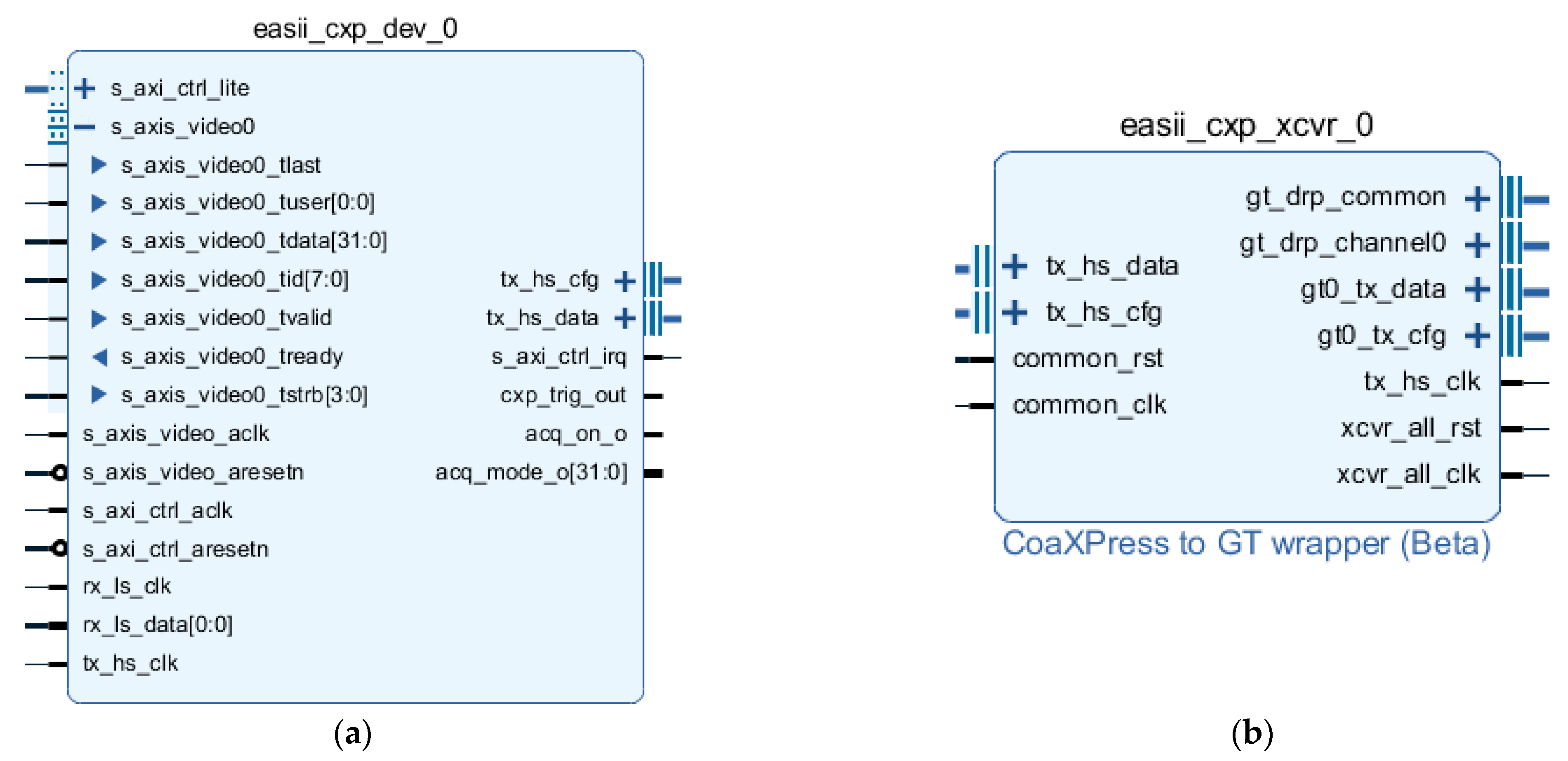
Figure 3 shows the CoaXPress interface modules (Cxp IP device and CxP Transceiver Controller). These connect the image sensor data from the CMOS sensor (Figure 2, right side) with the host or frame grabber (Figure 2, left side). Figure 3a shows the interface ports of the Cxp device module. It has a control AXI4-Lite interface, which is used to monitor and control all user memory space, and an AXI4 slave video stream interface dedicated to image data transfer from the TuMag sensor driver to the host. Table 2 shows an interface port description. The uplink and downlink data interface is connected to CoaXPress through the Artix 7 FPGA GTP transceiver and Cxp Transceiver Controller module, see Figure 3b. Table 3 shows interface port descriptions. The output of the GTP transceiver is connected to physical media through a Microchip chip [14].
Additionally, the CoaXPress interface supports the Generic Interface for Cameras or GeniCam standard [15]. It permits decoupling industrial camera interface technology such as CMOS sensor GSENSE400BSI from the user application programming interface (API). This standard support is conducted through an XML file stored in the device. This file is shared with the host at the time of connection and thus provides a description (namespace given by the standard) of the GeniCam API-compliant device (GenAPI). The boot records, stored on the Cxp device, provide the frame grabber with a way to access the XML file.
The TuMag-ECS CoaXPress communication interface has been tested using a commercial frame grabber installed on a PC (Euresys Coaxlink Quad frame grabber). Through it and for debugging purposes only, we have checked the operation of all the camera functionalities.

2.1.2. Heater Module
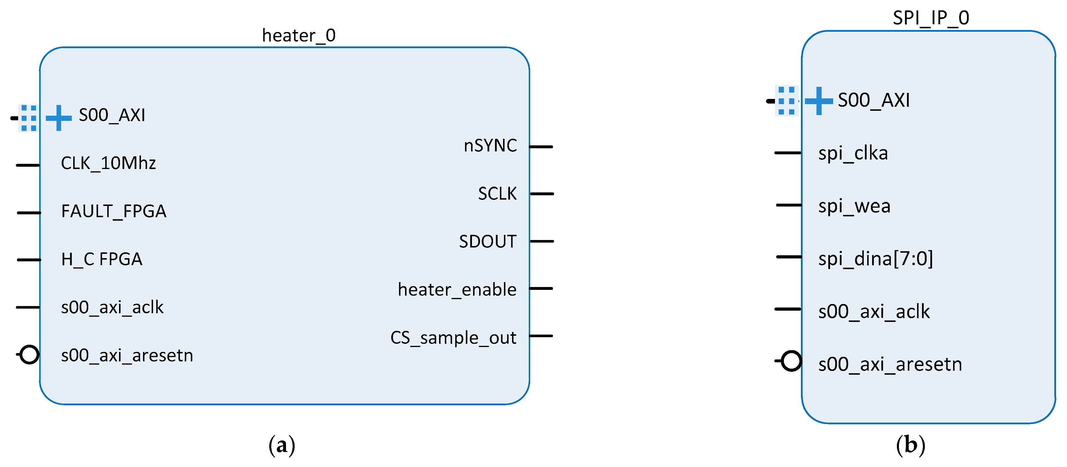
This module (Figure 4a) is necessary for the thermal control of the CMOS Sensor. Basically, a Peltier/heater device is included in the sensor PCB. The thermal control is performed by means of 4 commands managed by the host. These commands are sent from the frame grabber or host and the software of the TuMag embedded control system decodes them into local actions like setting the temperature setpoint value, enabling and disabling the heater, or reading the heater status. The heater control IP core configures, via SPI, the Texas Instruments DAC8311IDCKT [14] (Table 4). The SPI clock is limited to a maximum frequency of 1 MHz due to path restrictions. The heater core has a timer configured to periodically (every second) refresh the DAC to prevent it from losing its configuration and desired temperature and set point value.

2.1.3. SPI Module

For the GSENSE400 BSI CMOS detector, after the power-up or reset sequence, the default values for all on-chip registers are ‘0’. These registers should be re-programmed. The sensor driver module (Figure 1) has an integrated FSM (finite state machine) to perform read and write (re-programming) operations on the 256 bits of the internal register. Both operations are performed at a frequency of 25 MHz coming from the detector. These read-and-write sequences cannot be interrupted by each other, i.e., all 256 bits have to be read or written without interruption.
In the write operation, the FSM takes the data from the RB2 register and reprograms the internal register of the sensor. In the read operation, FSM reads the data from the sensor (organized as 32 8-bit registers) and stores it in the SPI module. The architecture of this IP is based on a dual real port BlockRam. It is wrapped with an AXI4-Lite interface on the MicroBlaze side and an 8 data bit on the SPI sensor side (Table 5). In this way, the memory decouples the clock domain of the sensor driver from the clock domain of the AXI4-Lite interface. Figure 4b shows the IP interface.

2.1.4. Train Module

The CMOS sensor has a train operation mode that permits alignment/calibration of the incoming 12-bit 8-channel serial data from the sensor. Training is run at the start of the firmware embedded software or upon request of the host. This training task is performed in the sensor driver block (Figure 1) and monitored by the train module (Table 6). When bit, word, and channels alignment is achieved, a status report is generated and sent to the instrument host. The training is repeated until all data channels are calibrated. Figure 5a depicts the train module interface.

2.1.5. XADC Module

This IP (inside of FPGA device) was used to monitor the internal FPGA on-chip register values such as on-chip temperature reg, on-chip VCCINT data reg, on-chip VCCAUX data reg, ADC out of VP/VN, on-chip VREFP data reg, on-chip VREFN data reg, and VBRAM data (Table 7). Figure 5b shows the IP block port interface. These measurements need to be known to be able to properly correct camera frames from dark current or gain fluctuations. Figure 5b depicts the XADC module interface.

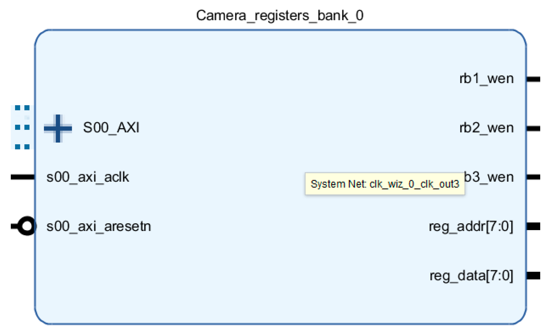
2.1.6. AXI_to_Camera Register Module

The embedded software application configures and controls the operation of the CMOS through the AXI_to_Camera register module (Figure 6). To do this, the module has three register memory banks, RB1, RB2, and RB3, for storing the configuration parameters of the sensor driver. The RB1 register bank is used to control the data acquisition process, set the sensor in calibration, acquisition, or test mode, store the calibration words, and store the words for testing the sensor in test mode. The RB2 register bank stores the 256 bits sensor register for configuration through the FSM circuit integrated in the sensor driver module. RB3 is a register bank used by the image decoder module (in the sensor driver block) to generate the timing control signal for image acquisition. Table 8 shows the interface ports description of the camera register banks module.

2.2. TuMag Embedded Software Application

The TuMag camera has a set of hardware registers through which it is possible configure the acquisition process, as well as the conditions under which it is conducted. In addition, the camera has another set of registers that allow the monitoring/controlling of other system parameters, such as the FPGA input voltage or the internal sensor temperature.
The embedded application software was developed using Xilinx SDK IDE in the C programming language and under the GeniCam standard. This application, which runs continuously on the MicroBlaze soft processor, has the functionalities of initializing local FPGA registers into driver module and sensor configurations FPGA register banks (RB1, RB2, and RB3), establishing the communications system link and speed between the frame grabber (host) and the device for data acquisition (sensor), updating (to shared) the XML file (GeniCam camera standard specification) on the host, setting the interrupt map in the embedded system memory, and decoding the commands coming from the host.
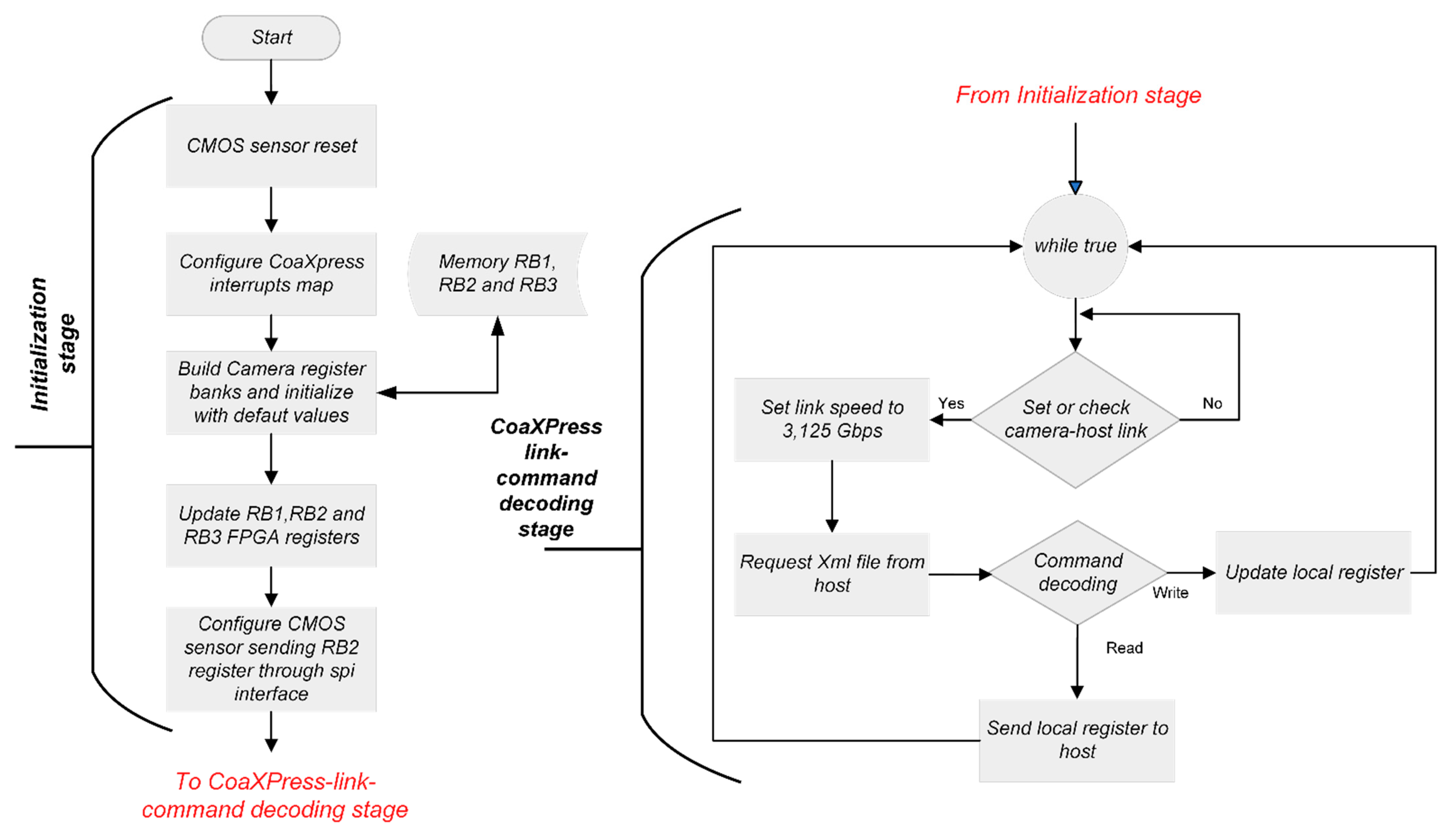
Figure 7 depicts a simplified flow diagram of the main code. We can differentiate two stages: the initialization stage (Figure 7 to the left) and the CoaXPress link-command decoding stage (Figure 7 to the right).
In the initialization stage, the application sets the CMOS sensor to the reset state, configures the CoaXPress interrupts map on MicroBlaze memory, builds and initializes the camera register banks (RB1, RB2, and RB3) on memory with default values, updates the RB1, RB2, and RB3 FPGA register into sensor driver modules, and configures the CMOS sensor with default values of the RB2 register.
In the CoaXPress link-command decoding stage, the application goes into an infinite listening loop where the device–host is linked through a discovering process, where the communication speed is set to 3125 Gbps, and where the GeniCam XML file format of the TuMag camera is exchanged with the host. This XML file, defined under the rules of the GeniCam standard, defines the configuration parameters, i.e., features of and commands of the TuMag camera, and permits the decoupling of sensor technology from the host application. The XML file, compressed in zip format, used in this design is organized in three categories: device control, image format control, and acquisition control. Within each of these categories there are different entries or registers. Each register, defined according to the GeniCam standard, has a name, an address, an access mode (Read only or Read/Write), a data type (command, integer, float, string, enumerated), and valid or allowed values. Table 9 shows some input values in the three categories.
The command decoding algorithm works like a “look at table”. In the MicroBlaze memory, all GeniCam entries used are defined with their name, address, and value. The software listens for an interruption coming from the host. When this happens, four parameters are read from the CoaXPress device, the device identifier, the command (cmd), the address (addr), and the size of the message (size). From the value of the cmd, the algorithm decides whether it is a write or read operation.
In the first case (writing cmd = 0 × 01, hexadecimal format), the data are read from the CoaXPress device y with the addr variable, and the “look at table” is searched to update the parameter (i.e., image) with the data value. The write-host commands permit updating the local FPGA registers RB1, RB2, and RB3, setting the temperature value of the heater circuit, configuring the internal CMOS registers, running the sensor training process, setting the camera in acquisition (continuous, single frame or CoaXPress) or test mode, and setting the sensor power ON/OFF.
In the second case or read command, cmd equals 0 × 00, the variable address is used to read the parameter and store variable data to be sent to the host (i.e., addr = 0 × 3028 data < −300 ms). Just like the write operation, the host can access the FPGA parameter values.
In both cases, write and read operations, the algorithm command decoding handles the errors through an ack variable in the following way. By default, the value of the variable is an invalid address or FALSE. If the decoded address is valid, the ack variable is updated as a valid address or TRUE. At the end of the address decoding process, the ack variable is sent with the appropriate value.
In the camera observation mode or CoaXPress mode (24 frames per second), image acquisition is controlled directly by the host. The principle of operation of the acquisition process is as follows: the host sends the trigger command and the CoaXPress device (Figure 2) generates the HW trigger signal and sends it to the sensor driver.
This signal is used to start or enable an FSM that controls the sensor readout cycle. This cycle consists of three phases: resetting rows, waiting for the configured exposure time, and eventually reading out in row order [14]. Figure 8 depicts a VHDL hardware simulation of the acquisition process in the sensor driver of Figure 2, showing only 32 rows for the compressed view. After the HW trigger signal is received, the sensor driver module controls the acquisition process by generating the image request signal (frame_req set to high red signal in Figure 8) and generating the time signals to synchronize the data readout (blue signals in Figure 8). The sync_x signal sets the data reading rate on the GPIXEL sensor device and, when the fval signal is set to 1, controls the time period where the data are available to be transmitted to the host. After the last line, the lval signal is transmitted, the grab_done signal (red in Figure 8) is set to high, and the sensor driver control goes into an idle state, waiting for a new HW trigger or command from the host.

2.3. Test Bench Software Application

Each flight and spare camera are later subjected to the following test campaign to ensure its functionality:
  • Optical characterization under ambient conditions (∼25 °C and 1 bar).
  • Optical and electrical characterization under near-vacuum conditions and three temperatures (hot, nominal, and cold). This provides confidence that the camera behaves correctly if there is no degradation with respect to the first step. No early component failures (“infant mortality”) have arisen from that first stress.
  • A bake-out for the elimination of all particles that could degrade the optics of the instrument. The camera is not yet supplied but kept at 60 °C for 72 h and 5 mbar of pressure.
  • A thermo-vacuum test (three temperatures: hot, nominal, and cold) to verify that the camera temperatures meet the thermal requirements (image sensor, FPGA, and cold finger temperatures are read by the camera itself; the temperature sensors placed on the camera cover are read by the test setup).
  • Finally, a second optical characterization gives us confidence in its behavior, before delivering the camera for assembly into the instrument.
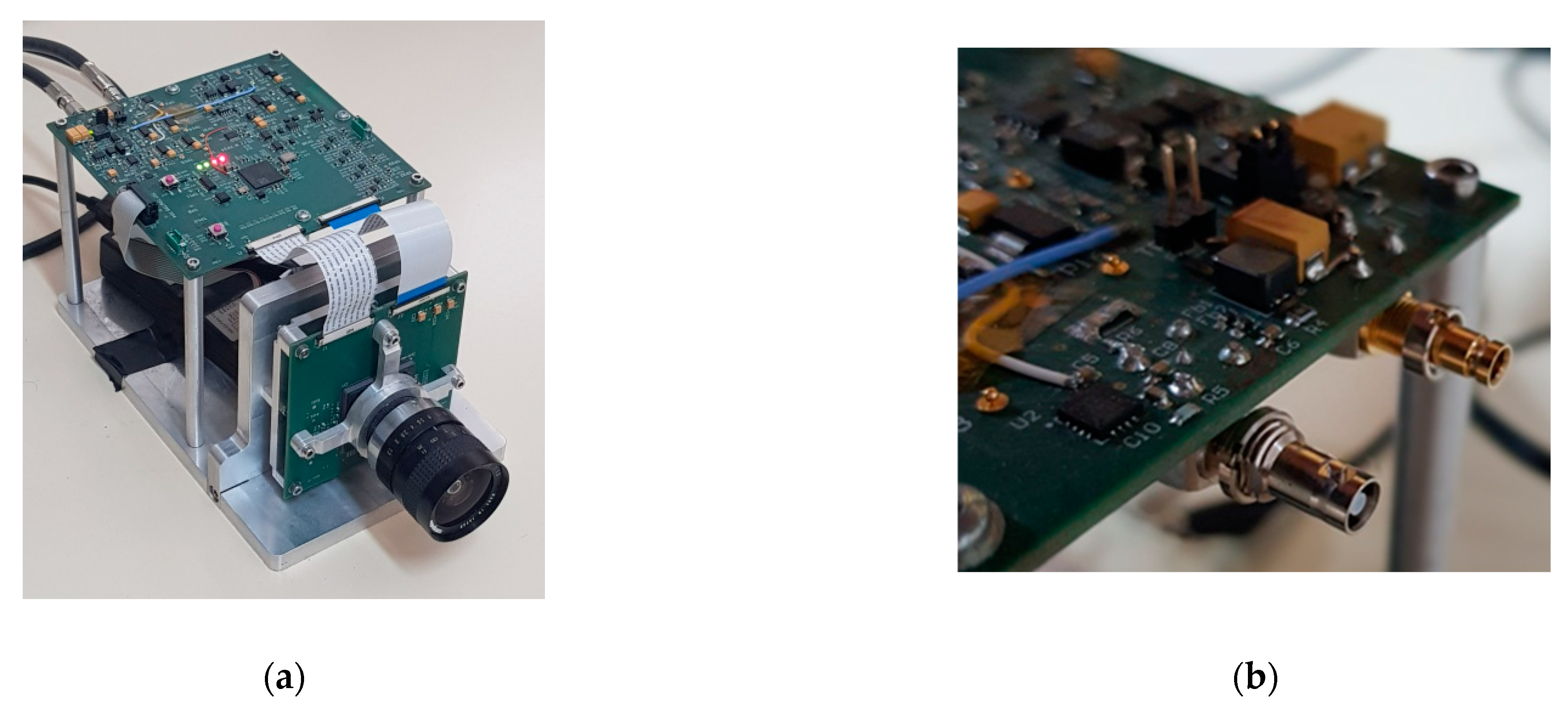
The TuMag cameras (Figure 9) are a critical subsystem of the instrument. To avoid risks in the transport of the complete instrument between the different laboratories where the testing campaigns were carried out, we designed and implemented a test-bench software application (TBSA) to handle the TuMag camera from a local computer. This allowed us to simplify the number of devices to be transported and reduced the assembly time of experimental setups. Due to the fact that each laboratory of the research consortium has this tool at its disposal, we only moved the camera and its associated electronics between the different laboratories to be characterized.
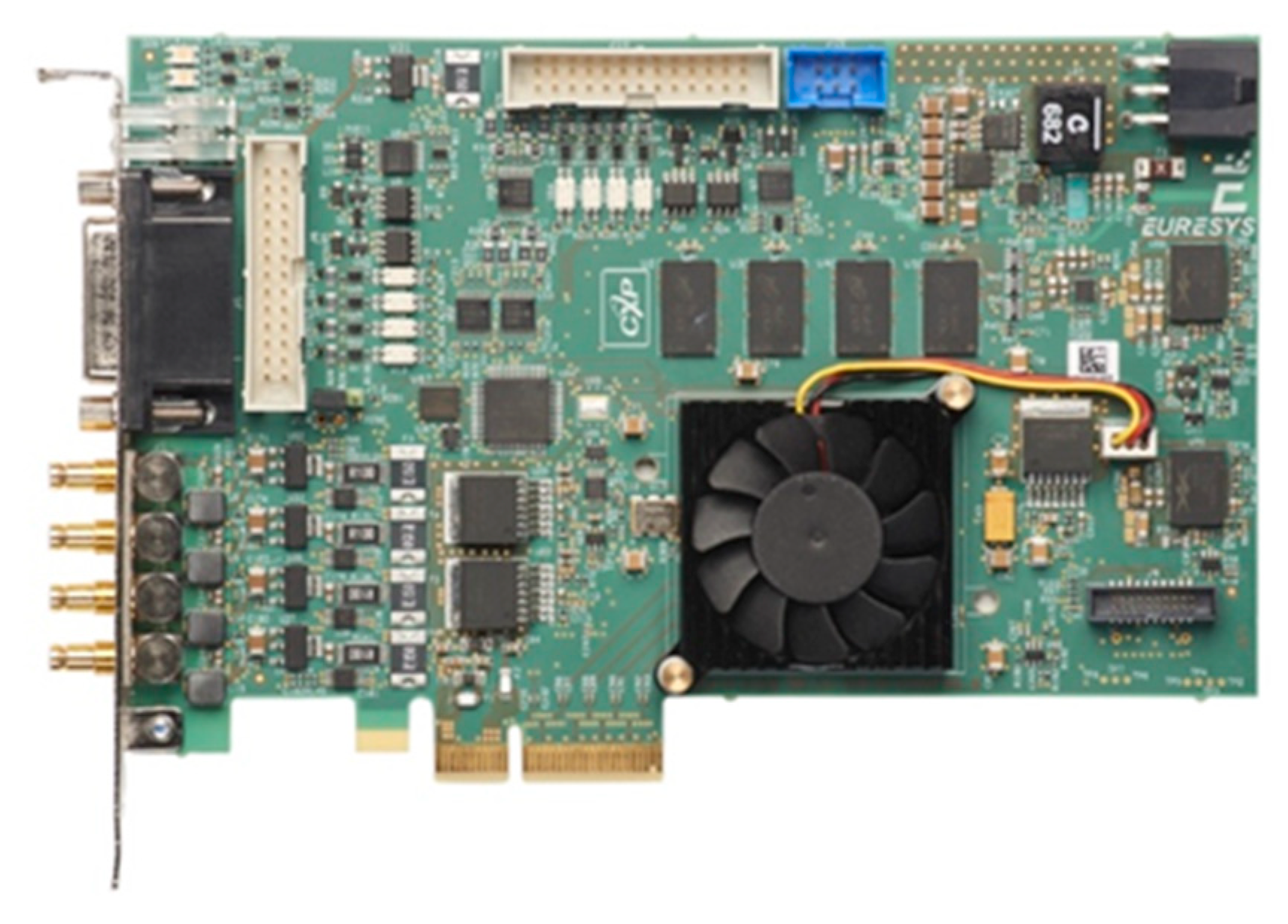
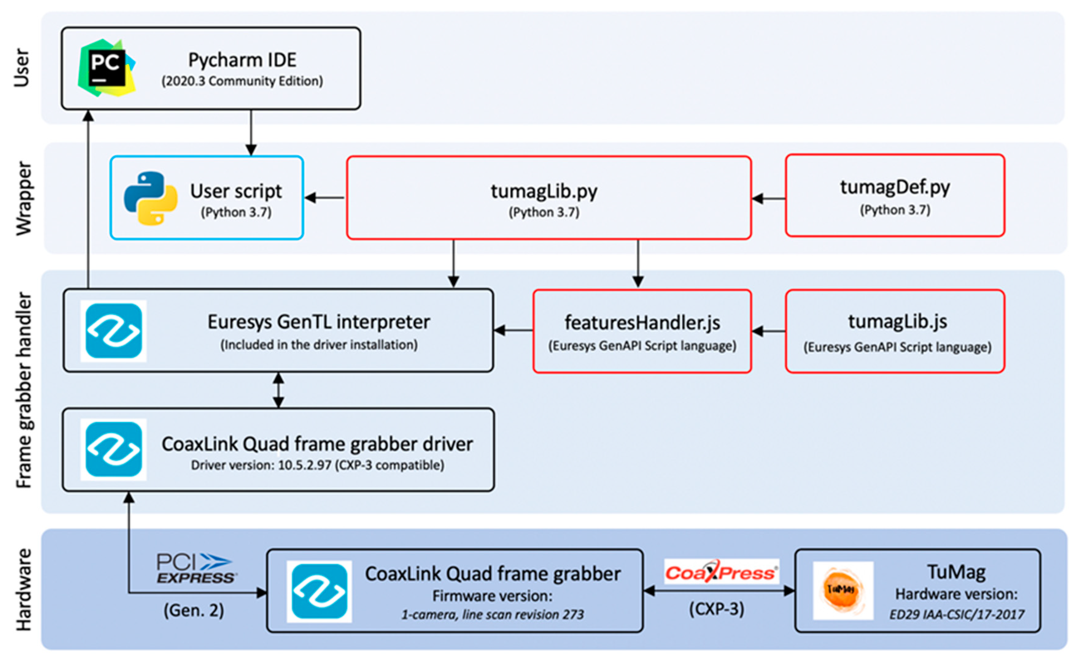
This TBSA, formed by a set of methods developed in Python and Java scripts, handles the Coaxlink Quad card, a trade frame grabber provided by Euresys Company installed on a personal computer. This card permits the streaming of images and configures, controls, triggers, and powers multiple high-speed cameras via CoaXPress 1.1 interface technology and GenICam programming interface (Figure 10).
Euresys Company provides its own GenAPI script language (like JavaScript) for programming modules and scripts to handle the features of frame grabbers and cameras based on GenICam. To adapt this generic software architecture to the TuMag camera, we implemented the tumagLib.js and the featuresHandler.js scripts. The first file defines a set of functions implemented to read, write, and execute the TuMag features. The second file contains the program used to handle the instrument. Figure 11 shows a block diagram representing the hardware and software architecture of TBSA used to handle the TuMag camera.
When the featuresHandler.js is launched, the frame grabber and the TuMag camera are automatically detected first, and then the script is executed. To write, read, and execute different TuMag features, this script must be modified to add the corresponding functions defined in the tumagLib.js module. For this, the user can use any text editor. In particular, the featuresHandler.js script is executed using the GenTL Console tool, which includes a GenTL interpreter specific to the Euresys GenAPI script language.
In addition, to improve the interaction and interface between the user and the hardware, we have developed a wrapper library developed in Python. Specifically, the wrapper consists of two files: tumagDef.py and tumagLib.py (Figure 11). The first one contains a list of the function names that are defined in the tumagLib.js module. It also includes the definition of paths to the necessary program files and required opcodes to generate system instructions automatically. The second file contains a set of functions to access and configure each of the available TuMag features. These Python functions automatically modify the script contained in featuresHandler.js to add the appropriate code and directly execute the corresponding system instruction to launch the Euresys GenTL interpreter.
This Python library is formed by the get, set, and execute functions, as well as initlib. Table 10 shows the Set/Get actions of the library grouped by functionalities. We have developed a user guide (the document is available on request from the authors) where the installation of the library, CoaXPress card and drive installation, and examples of the utilization can be found.
The results are displayed in the terminal console. As an example of use, 
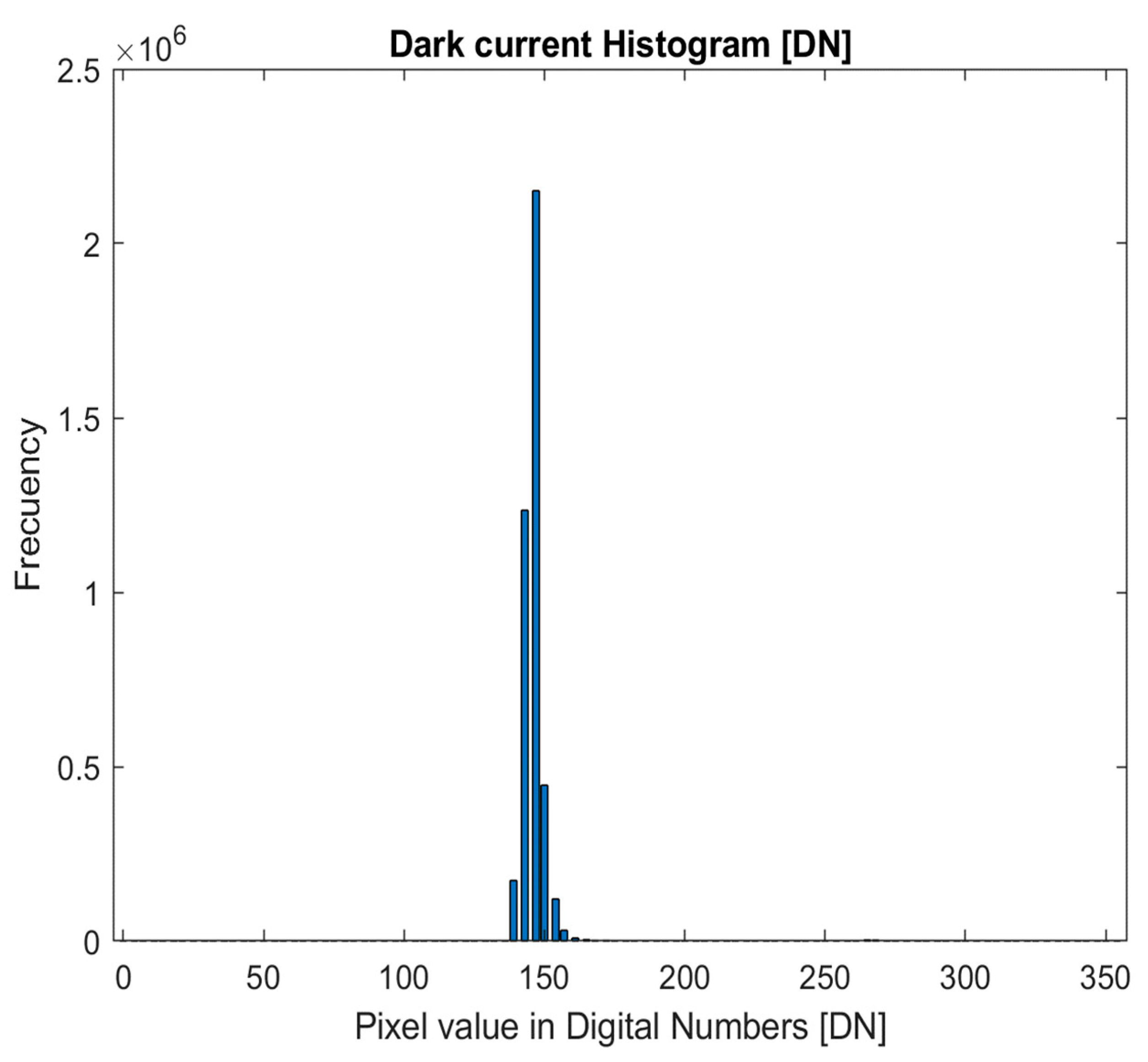
Figure 12 shows a block diagram of steps to measure Dark Image Characterization. The measurement process, defined in the Python script, is a succession of commands sent by the host to be decoded by the TuMag camera. It ends when all the gains and integration times are executed. Acquired images are sent to the host as they are captured.

3. Results

In this paper, we have presented the implementation of a specifically tailored FPGA architecture for the TuMag camera embedded control system and test-bench software application for carrying out thermal TuMag camera tests under controlled laboratory conditions. Both developments comply with the CoaXPress and Genicam standards. The TuMag-ECS was designed using HDL languages and implemented in an Artix-7 XC7A50T-2CSG325C FPGA device. The design was completed using Vivado and SDK 2017.4 for simulation, debugging, and implementation. The design was successfully integrated into the sensor driver board FPGA and is fully operational.
The TuMag-ECS in combination with software handles communication with the host for both commands and data transfer (24 frames per second) over a CoaXPress communications interface up to 3125 Gbps. In addition, TuMag-ECS manages bit, word, and serial channel camera calibration, configuration of internal detector registers such as region of interest (RoI) size, exposure time, hardware triggering, single or continuous acquisition modes, sensor gain, and black level offset adjustment. Also, TuMag-ECS manages the control temperature circuit of the sensor PCB, monitors FPGA parameters, and switches the sensor power ON/OFF.
The test-bench software application was implemented and tested. The TBSA tool, in addition to avoiding risks and costs in transporting the instrument, permits the reduction of the setup time of the different characterization processes on the TuMag Camera. All camera functionalities, architecture modules, and sensor configurations were successfully tested according to scientific requirements using a commercial frame grabber with a CoaXPress interface.
From the point of view of resources consumed by the Artix 7 FPGA (Table 11), most of them are below 25%, except for input/output operations which require 54%, the BUFG global clock buffers (56%), and the Mixed-Mode Clock Manager MMCM (80%). In these conditions, the employed FPGA still has enough resources to implement additional functionalities for camera frame pre-processing before the data are sent to the host.
The camera measurements can be divided into three clearly defined stages: the conversion of photons into electrons, the transformation of electrons into voltage, and, ultimately, the digitization of this voltage. Each of these stages introduces measurement noise, the source of which must be thoroughly comprehended to effectively address or reduce its impact [5]. The characterization of the TuMag camera noise was carried out using two tests, Dark Image Characterization and Linearity and Gain Assessment. In the first one, there was a sequence of dark images (5000) at different sensor gains. And the second one, also at different sensor gains, was illuminated with LED light (530 nm). For each gain setting, a sequence of 30 different exposure times was recorded, incrementally increasing from 0.0205 milliseconds up to the point of reaching the sensor’s full well capacity, which is dependent on the specific gain mode.
Table 12 shows a summary of the inferred noise parameters for different multiplicative sensor gains, where g is the gain or digital numbers by electrons, Nr is the readout noise due to the conversion of photons into electrons, and ∆/12 is the quantization noise, the quantization interval is ∆ = Dr/2n, with Dr being the dynamic range (the pixel full well expressed in DN), fprnu is the photon response non-uniformity associated with the sensor manufacturing, Ndc, fpn represents noises associated to dark current, that is, shot noise and fixed pattern noise resulting from pixel-to-pixel differences on manufacturing materials and alike, L is the linearity or measure of the dispersion of the fits, and SDC is the signal due to dark current. A few dust particles were identified in the regions exhibiting anomalous low signal levels. The number of pixels covered by dust particles remained below 0.001% of the whole image for all the cameras.
Figure 13 shows the results of acquiring a 2048 × 2048 image frame with the TuMag prototype laboratory camera. The USAF resolution test chart was used as a target.
Figure 14 depicts a histogram of the image signal in non-illuminated conditions, with an exposition time of 600 ms, and under vacuum and temperature-controlled conditions (25 °C). The mean value (149 DN) represents the dark current; it represents a constant offset of the image signal.

4. Conclusions

Merely conducting a market survey is often inadequate for finding a camera that meets the required specifications. Scientific demands typically diverge significantly from commercial needs [11,16]. This has indeed been the case during the initial stages of conceptualizing our two instruments for the SUNRISE III mission.
By conducting comprehensive tests and hardware and software design, a thorough understanding of the TuMag camera’s operational capabilities and performance characteristics was achieved, facilitating its effective deployment in scenarios resembling the SUNRISE III mission conditions. Also, the satisfactory results obtained in the battery of tests performed on TuMag show that the technologies used can be exploited for the design and implementation of new solar instruments. Such is the case that this embedded system and test-bench software application has also been used in the implementation of the SCIP (Sunrise Chromospheric Infrared spectroPolarimeter) instrument [5].
The GSENSE400-BSI detector is a relatively new scientific image sensor with a high dynamic range, high sensitivity, and low noise. The designs, based on this image sensor, found in the literature [17,18] are usually based on other communication interfaces such as camera links or USB. Our design used a CoaXPress communications interface with better mechanical and electrical performance (a simple coaxial cable to data and commands simplifies the connection to the host and signal-to-noise reduction). Considering that the TuMag camera must be in vacuum conditions, a serial connection, between camera and host, is more efficient than a parallel connection [19].
The attainable signal-to-noise ratio within a system subjected to illumination conditions wherein shot noise, directly proportional to the square root of the signal magnitude, predominates as the primary contributor to measurement interference is of particular significance. Consequently, the aim is to mitigate the influence of other noise sources that scale linearly with the signal magnitude. This mitigation strategy is accomplished by ensuring that the detector’s filling level remains below fifty percent of its capacity.

Supplementary Materials

The following supporting information can be downloaded at: https://www.mdpi.com/article/10.3390/electronics12194071/s1. The block diagram of all TuMag-ECS circuits.

Author Contributions

Conceptualization, D.O.S., M.R.V. and D.H.E.; methodology, M.R.V., D.H.E. and E.M.C.; software, M.R.V.; validation, D.O.S., D.H.E., M.R.V. and E.M.C.; formal analysis, M.R.V., D.O.S. and D.H.E.; investigation, M.R.V., D.O.S. and E.M.C.; writing—original draft preparation, M.R.V. and D.O.S.; writing—review and editing, M.R.V. and D.O.S.; supervision, D.O.S., M.R.V. and B.R.C. All authors have read and agreed to the published version of the manuscript.

Funding

This research was funded by the RTI2018-096886-B-C53 Project of the Ministry of Science.

Institutional Review Board Statement

Not applicable.

Informed Consent Statement

Not applicable.

Data Availability Statement

Not applicable.

Conflicts of Interest

The authors declare no conflict of interest.

References

  1. Solanki, S.K.; Gandorfer, A.; Chares, B.; Curdt, W.; Deutsch, W.; Feller, A.; Del Toro Iniesta, J.C.; Orozco Suárez, D.; Martínez Pillet, V.; Hirzberger, J.; et al. The Sunrise III mission. Sol. Phys. 2023; in preparation. [Google Scholar]
  2. Feller, A.J.; Gandorfer, A.M.; Iglesias, F.A.; Lagg, A.; Riethmüller, T.L.; Solanki, S.K.; Katsukawa, Y.; Kubo, M. The SUNRISE UV Spectropolarimeter and imager for SUNRISE. In Proceedings of the Ground-Based and Airborne Instrumentation for Astronomy VIII, Online, 13 December 2020; Volume 11447. [Google Scholar] [CrossRef]
  3. Katsukawa, Y.; Iniesta, J.C.d.T.; Solanki, S.K.; Kubo, M.; Hara, H.; Shimizu, T.; Oba, T.; Kawabata, Y.; Tsuzuki, T.; Uraguchi, F.; et al. Sunrise Chromospheric Infrared SpectroPolarimeter (SCIP) for sunrise III: System design and capability. In Proceedings of the Ground-based and Airborne Instrumentation for Astronomy VIII, Online, 13 December 2020; Volume 11447. [Google Scholar] [CrossRef]
  4. Del Toro Iniesta, J.C.; Orozco Suárez, D.; Álvarez-Herrero, A.; Sanchis Kilders, E.; Pérez Grande, I.; Ruiz Cobo, B. TuMag: The tunable magnetograph for the Sunrise III mission. Sol. Phys. 2023; in preparation. [Google Scholar]
  5. Suárez, D.O.; García, D.; Jiménez, A.C.L.; Jiménez, M.B.; Expósito, D.H.; Labrousse, P.; Bailén, F.J.; Díaz, I.B.; Martínez, E.B.; del Moral, B.A.; et al. SPGCam: A specifically tailored camera for solar observations. Front. Astron. Space Sci. 2023, 10, 1167540. [Google Scholar] [CrossRef]
  6. Gpixel, Datasheet V1.5; GSENSE400 4 Megapixels Scientific CMOS Image Sensor; Gpixel: Changchun, China, 2017.
  7. Ma, C.; Liu, Y.; Li, J.; Zhou, Q.; Chang, Y.; Wang, X. A 4MP high-dynamic-range, low-noise CMOS image sensor. In Proceedings of the Image Sensors and Imaging Systems, San Francisco, CA, USA, 13 March 2015; Volume 9403. [Google Scholar] [CrossRef]
  8. Wang, F.; Dai, M.; Sun, Q.; Ai, L. Design and implementation of CMOS-based low-light level night-vision imaging system. In Proceedings of the Seventh Symposium on Novel Photoelectronic Detection Technology and Applications, Kunming, China, 12 March 2021; Volume 117635. [Google Scholar] [CrossRef]
  9. IC/130206 (EASii IC); Hard Soft Interface Document. CoaxPress Device IP Specification: Mansfield, TX, USA, 2017.
  10. Xilinx, 7 Series FPGAs Data Sheet: Overview. Product Specification. DS180 (v2.6.1). 2020. Available online: https://www.xilinx.com/support/documentation/data_sheets/ds180_7Series_Overview.pdf (accessed on 2 December 2020).
  11. Zhang, Y.-H.; Zhang, H.-F.; Qu, W.-Q.; Wang, Z.-Y.; Zhu, Z.-Y.; Zhu, J.; Zhang, J.; Chen, J.-T.; Feng, Y.; Jia, M.-H.; et al. Design of a large-format high-rate scientific CMOS camera. In Proceedings of the Society of Photo-Optical Instrumentation Engineers (SPIE) Conference Series (SPIE), Online, 13 December 2020; Volume 1145407. [Google Scholar] [CrossRef]
  12. CoaXPress Standard for High-Speed Imaging in Professional and Industrial Imaging Applications. Available online: https://www.coaxpress.com/ (accessed on 20 October 2019).
  13. Byte Oriented DC Balanced 8B/10B Partitioned Block Transmission Code. U.S. Patent 4486739, 4 December 1984.
  14. Valido, M.R.; Orozco Suarez, D.; Del Toro Iniesta, J.C.; Balaguer Jimenez, M.; Magdaleno Castello, E.; Hernandez Exposito, D.; López Jiménez, A.C.; Álvarez García, D.; Ruiz Cobo, B. TuMag/SCIP Cameras FW CIDL Document (SR3-IMAXP-LI-SW730-001); Instituto de Astrofísica de Andalucía: Granada, Spain, 2020. [Google Scholar]
  15. GenICamTM Standard from the European Machine Vision (EMVA), GenICam Package Version 2018.06. Available online: http://www.emva.org. (accessed on 20 October 2019).
  16. Zhu, J.; Zhang, H.-F.; Zhang, Y.; Tang, Y.; Zhu, Z.; Zhang, J.; Zeng, F.; Liu, H.; Wang, J.; Ge, J. Design of a scientific CMOS camera for astronomical observation. In X-ray, Optical, and Infrared Detectors for Astronomy X; Holland, A.D., Beletic, J., Eds.; SPIE: Montréal, QC, Canada, 2022; Volume 1219126. [Google Scholar] [CrossRef]
  17. Zhang, H.; Ma, Q.-J.; Wang, S.-R. High speed CMOS imaging electronics system for ultraviolet remote sensing instrument. Opt. Precis. 2018, 26, 471–479. [Google Scholar] [CrossRef]
  18. Tang, X.; Liu, G.; Qian, Y.; Cheng, H.; Qiao, K. A handheld high-resolution low-light camera, In Proceedings of the Fifth Symposium on Novel Optoelectronic Detection Technology and Application, Xi’an, China, 12 March 2019; Volume 11023. [CrossRef]
  19. McCurrach, B. A Quick Overview Of Industrial Camera Interfaces. Quality 2022, 61, 31. [Google Scholar]
Figure 1. TuMag camera FPGA blocks diagram.
Electronics 12 04071 g001
Figure 2. TuMag-ECS blocks diagram architecture. The AXI Interconnect manages the AXI transactions between the AXI Master (MicroBlaze) and the AXI Slaves modules.
Electronics 12 04071 g002
Figure 3. Block diagram of the embedded CxP control interface. (a) CoaXPress IP controller; (b) wrapper interface to the GTP FPGA transceiver.
Electronics 12 04071 g003
Figure 4. (a) Block diagram of the interface of the heater module. (b) Block diagram of the interface of the SPI module.
Electronics 12 04071 g004
Figure 5. (a) Block diagram of the train module; (b) module to monitor 24 V circuit power.
Electronics 12 04071 g005
Figure 6. Block diagram of camera registers memory bank.
Electronics 12 04071 g006
Figure 7. Flow diagram of embedded application software.
Electronics 12 04071 g007
Figure 8. Waveform diagram of simulation frame request from the host. We only show the 32-line readout to illustrate the process of acquiring an image.
Electronics 12 04071 g008
Figure 9. (a) Photograph of a TuMag camera laboratory prototype. (b) Photograph of the connectors of the TuMag prototype for data transmission and power input.
Electronics 12 04071 g009
Figure 10. Photograph of a CoaXPress frame grabber used for the test-bench software application.
Electronics 12 04071 g010
Figure 11. Block diagram of the hardware and software architecture, including the Python wrapper for TBSL.
Electronics 12 04071 g011
Figure 12. Simplified block diagram of the pipeline commands to characterize.
Electronics 12 04071 g012
Figure 13. Acquired image in digital number (DN) using a USAF pattern.
Electronics 12 04071 g013
Figure 14. Sensor dark current histogram in digital number (DN).
Electronics 12 04071 g014
Table 1. List of the key specifications of GSENSE400BSI [11].
ParameterValue
Optical format2.0 inch
Active image size22.528 × 22.528 (mm)
Pixel size11 × 11 µm
Number of active pixels2048 (H) × 2048 (V)
Shutter typesElectronic rolling shutter
Frame rate24 fps @ HDR mode48 fps @ STD mode
Full well capacity90 ke
Temporal dark noise1.6 e
Dark current0.2 e/s/pix@−50 °C
Output format8 pairs of LVDS drivers
Package115 pins
Power Consumption<650 mW
ChromaMono
Table 2. Port descriptions of the CoaXPress IP controller.
Port NameI/O PortDescription
s_axi_ctrl_liteI/O BusAXI4-Lite interface containing write and read channels
s_axis_video0I/O BusAXI video data channel
s_axis_video0_tlastILast data for current line
s_axis_video0_tuserIStart of image information
s_axis_video0_dataICXP pixel-packed data bus
s_axis_video0_tidITID of the current stream
s_axis_video0_tvalidIData valid information from master
s_axis_video0_treadyOSlave ready to accept data
s_axis_video0_tstrbIPixel/Metadata information
s_axis_video_ackIAXI4-Stream common clock, 125 MHz
s_axis_video_aresetnIAXI4-Stream common synchronous active-low reset
s_axis_ctrl_aclkIClock input—no special frequency restriction
s_axis_ctrl_ aresetnIActive low reset input
rx_ls_clkIFixed 125 MHz clock input
rx_ls_dataI20.833 Mbps data from equalizer
tx_hs_clkISerDes clock 125 MHz
tx_hs_cfgI/O BusSerDes configuration bus
tx_hs_dataI/O BusUplink and Downlink port
s_axi_ctrl_irqOSynchronous rising edge interrupt
cxp_trig_outOHw trigger from host
Table 3. Port descriptions of the wrapper interface to the GTP FPGA transceiver.
Port NameI/O PortDescription
tx_hs_cfgI/O BusSerDes configuration bus
tx_hs_dataI/O BusUplink and Downlink port
common_ rstICommon Axi reset
common_clkI50 MHz Common Axi clk
gt_drp_commonI/O BusDynamic reconfiguration port Configuration
gt_drp_channel0I/O BusDynamic reconfiguration port, channels
gt0_tx_dataI/O BusGtp transmitter data interface
gt0_tx_cfgI/O BusGtp transmitter configuration interface
tx_hs_clkOSerDes clock from 125 MHz
xcvr_all_rstORest to GPTtransceiver
xcvr_all_clkO100 Mhz to GPT transceiver
Table 4. Port descriptions of the heater module.
Port NameI/O PortDescription
S00_AXII/O BusAXI-Lite Interface
CLK_10 MhzI10 MHz clock
FAULT_FPGAIHeater Status. ‘1’ fault, ‘0’ heater status is correct
H_C_FPGAIHeater operation. ‘1’ warming up, ‘0’ heater cooling
s00_axi_aclkI50 MHz main axi clock
s00_axi_aresetnIAsynchronous low level clear
nSYNCODAC8311, enable signal
SCLKODAC8311 signal clock
SDOUTOSerial data signal (set point value) connect to Din of DAC8311
heater_enableOenable/disable Heater system
CS_sample_outOPeriodical Output signal for debug purpose
Table 5. Port descriptions of the SPI module.
Port NameI/O PortDescription
s00_axi_aclkI50 MHz main axi clock
s00_axi_aresetnIAsynchronous low level clear
S00_axiI/OAXI-Lite Interface
spi_din [7..0]Ispi data input
spi_clkI25 Mhz spi clk
spi_weOSPI write enable signal
Table 6. Port descriptions of the train module.
Port NameI/O PortDescription
s00_axi_aclkI50 MHz main axi clock
s00_axi_aresetnIAsynchronous low level clear
S00_AXII/OAXI-Lite Interface
train_dina [7..0]Ispi data input
train_clkInput25 Mhz spi clk
train_weaISpi write enable signal
training_doneIInput from training module
HW_TRAINOOutput to host hw training
Table 7. Port descriptions of the module to monitor 24 V circuit power.
Port NameI/O PortDescription
s00_axi_aclkInput50 MHz main axi clock
s00_axi_aresetnInputAsynchronous low level clear
S00_axiI/OAxi4-Lite Interface
Vp_VnIExternal differential input voltage
Table 8. Port descriptions of the camera register memory bank module.
Port NameI/O PortDescription
s00_axi_aclkInput50 MHz main processor axi clock
s00_axi_aresetnInputAsynchronous low level clear
S00_AXII/OAXI-Lite Interface
rb1_wenoutputSignal enable/select to write data in bank 1
rb2_wenoutputSignal enable/select to write data in bank 2
rb3_wenoutputSignal enable/select to write data in bank 3
reg_addr [7:0]outputBank Address to write data
reg_data [7:0]outputdata to be written into register banks
Table 9. XML entries for some camera features.
Xml Entry Name AddressValueAccess ModeType
Device control category
DeviceVendorName@0x2000EASii-ICROString
DeviceFirmwareVersion@0x20901.2r16ROString
Image Format Control category
WidthMax@0x30002048ROinteger
width@0x3024Default 2048RWinteger
PixelFormat@0x3014Mono16RWEnumerated
Acquisition Control Category
AcquisitionStart@ 0x300C1RWCommand
AcquisitionStop@ 0x30100RWCommand
ExposureTime @0x3028Default 300 msRWFloat
Table 10. Main functionalities of the implemented library.
SetGet
Heater functionsSet temperature value of heater, and enable or disable the heater module Get the actual status of de heater module
Training functionsEnables or disables trainingGet the result of the training process. For each of the 8 available channels
Sensor configuration functionsSet region of interest (ROI), gain, mode, integration time, sampling frequency, and set if multiple or single frame captureGet internal sensor register values, get ROI, Gain, integration time, and get sensor temperature
Acquisition process
execution functions
Executes image acquisition, i.e., continuous acquisition (Start/Stop) and acquisition via HW trigger or via SW trigger. Images are sent to the host/frame grabber
Miscellaneous functionsEnables or disables sensor power ON/OFF and camera reset Get internal FPGA register values: temperatures and voltages, get embedded hardware and software version
Table 11. FPGA resource utilization for TuMag-ECS architecture.
Component Used/AvailableUsed (%)
LUT4847/32,60015%
LUTRAM278/96003%
FF6023/65,2009%
BRAM18/7524%
IO81/15054%
GT1/425%
BUFG18/3256%
MMCM4/580%
Table 12. Noise parameters obtained from the prototype TuMag camera.
Sensor Gaing (DN/e)Nr (DN)∆/12 (DN)fprnu (%)Ndc, fpn (%)L (%)SDC (DN)
1.85×0.05201.7750,7111.670.490.20149.16 ± 0.68
2.49×0.07072.1342,2361.740.430.22149.22 ± 0.70
3.68×0.10342.3737,8991.870.180.34149.14 ± 0.82
1.29×0.03691.6155,9431.590.700.10148.25 ± 0.74
3.70×0.10282.6633,8281.860.400.39149.22 ± 1.10
Disclaimer/Publisher’s Note: The statements, opinions and data contained in all publications are solely those of the individual author(s) and contributor(s) and not of MDPI and/or the editor(s). MDPI and/or the editor(s) disclaim responsibility for any injury to people or property resulting from any ideas, methods, instructions or products referred to in the content.

