Article

A Capacitorless LDO Regulator with Fast Feedback Loop and Damping-Factor-Control Frequency Compensation

1
Institute of Microelectronics of the Chinese Academy of Sciences, Beijing 100029, China
2
University of Chinese Academy of Sciences, Beijing 100049, China
*
Author to whom correspondence should be addressed.
Electronics 2023, 12(19), 4067; https://doi.org/10.3390/electronics12194067
Submission received: 4 September 2023 / Revised: 22 September 2023 / Accepted: 24 September 2023 / Published: 28 September 2023

Abstract

:
A fast feedback loop (FFL) based on comparators is proposed in this paper. The FFL improves the transient response characteristics of the output-capacitorless low-dropout (OCL-LDO) regulator. When the load current switches between 1 mA and 100 mA with 1 μ s edge time, the overshoot and undershoot are 33 mV and 37 mV, respectively, and recovery time is 1.2 μ s and 1.6 μ s, respectively. A damping-factor-control (DFC) frequency compensation circuit is used to ensure the stability of the OCL-LDO, and the simulation results show that the phase margin exceeds 50 degree in the entire load variation range. This design is based on 180 nm process, and the area of the chip is 0.068 mm 2 (without pads). A band-gap reference circuit is also designed in this work; its output voltage is 1.2 V and its temperature coefficient is 7.96 ppm/ C. The input voltage range of the proposed OCL-LDO is 2.5 V to 5 V with a linear regulation rate of 0.128 mV/V and a load regulation rate of 0.0017 mV/mA. In addition, the load range of the proposed OCL-LDO is 0 mA to 100 mA, and the minimum required external capacitance is 0 F. The power supply rejection ratio (PSRR) is −46 dB @ 1 kHz.

1. Introduction

Low-dropout (LDO) voltage regulators play an important role in system-on-chip (SoC) design, due to its wide output voltage, low noise, high power supply rejection ratio, and fast load response [1,2,3]. In the traditional LDO structure, an external output off-chip capacitor ( C L ) usually in the μ F range is needed to stabilize the output voltage. Usually, C L requires extra pins, and it is not easy to integrate with other circuit modules due to the large on-chip area required. Thus, it is difficult to meet the current high-integration design requirements [4,5,6]. OCL-LDO has attracted more and more attention because it does not require additional large capacitors and is easy to integrate with other circuit modules.
Because OCL-LDO cannot compensate the loop through the zero point introduced by external ESR resistor and capacitor, it is necessary to design a special frequency compensation module. OCL-LDO has many frequency compensation methods, some commonly used methods are introduced in references [7,8,9,10,11,12]. The damping-factor-control (DFC) method redistributes the zero and pole points of the system by adding a damping control unit in the circuit. This method is effective for circuits with large capacitance nodes in the system, and can also improve the transient characteristics of the circuit [13,14,15,16]. In addition, the transient enhancement loop is very important for the OCL-LDO because of its small load capacitance. Reference [11] proposed a weighted current feedback (WCF) technique that can improve gain and loop stability. When the current changes from 0 to 50 mA, its recovery time is 250 ns, but it requires a capacitor of 0.47 μ F. Reference [15] proposed an LDO with an input range of 8 V to 24 V. Through DFC technology, it can maintain the stability of the loop without external large capacitors. However, its overshoot voltage is 118.8 mV, and its undershoot voltage is about 140 mV.
This paper is organized as follows. Section 2 shows the main circuit structure. Section 3 analyzes the frequency compensation. Section 4 summarizes the simulation results. Section 5 is the conclusion of this paper.

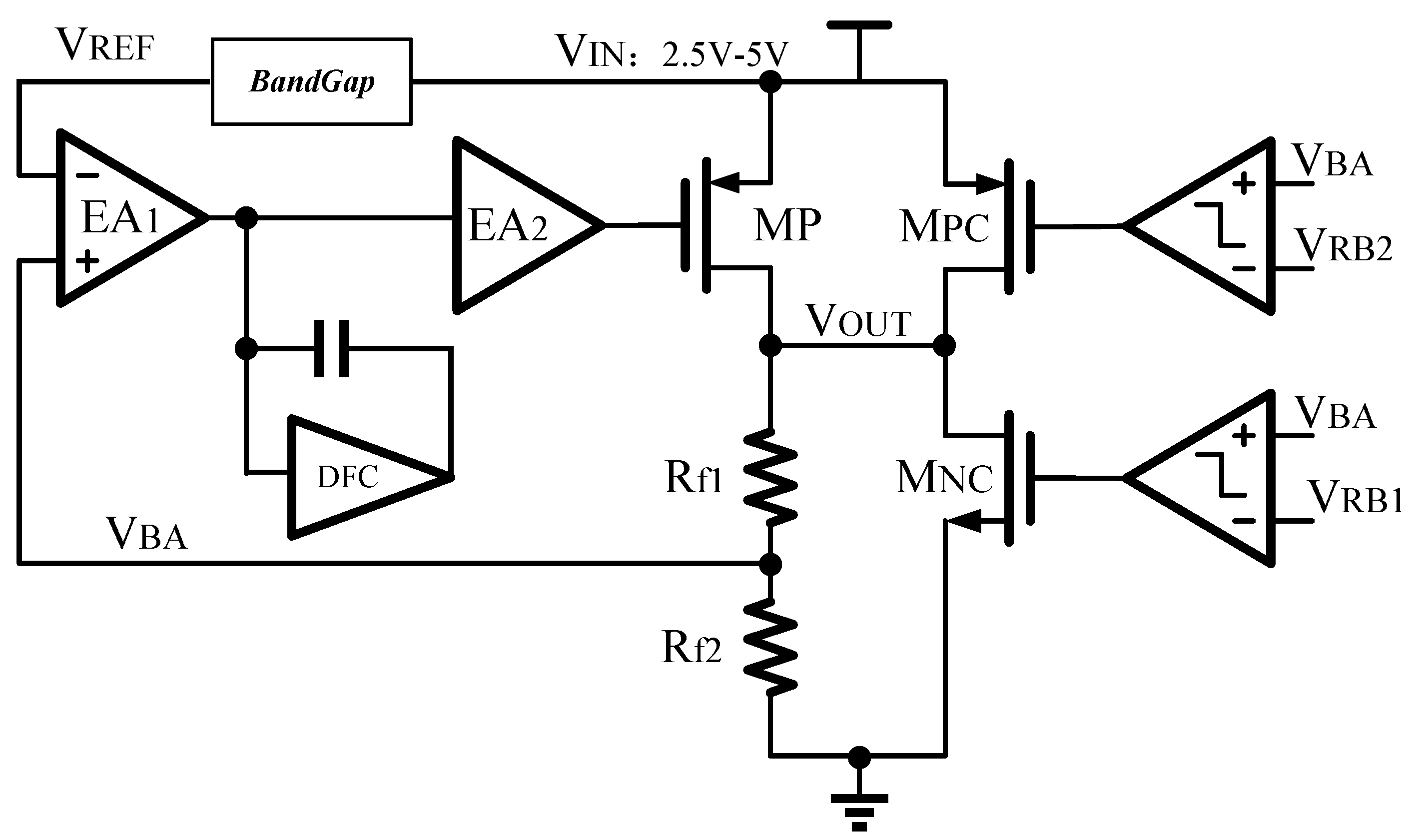
2. Circuit Implementation

In this work, an OCL-LDO with fast feedback loop is proposed. Figure 1 shows a simplified block diagram of the proposed OCL-LDO. The OCL-LDO includes a fast feedback loop [17,18,19], a reference circuit, an error amplifier for comparing the difference between the feedback and reference voltage, and a DFC provides frequency compensation [20,21,22]. A detailed circuit of the error amplifier and DFC is shown in Figure 2.

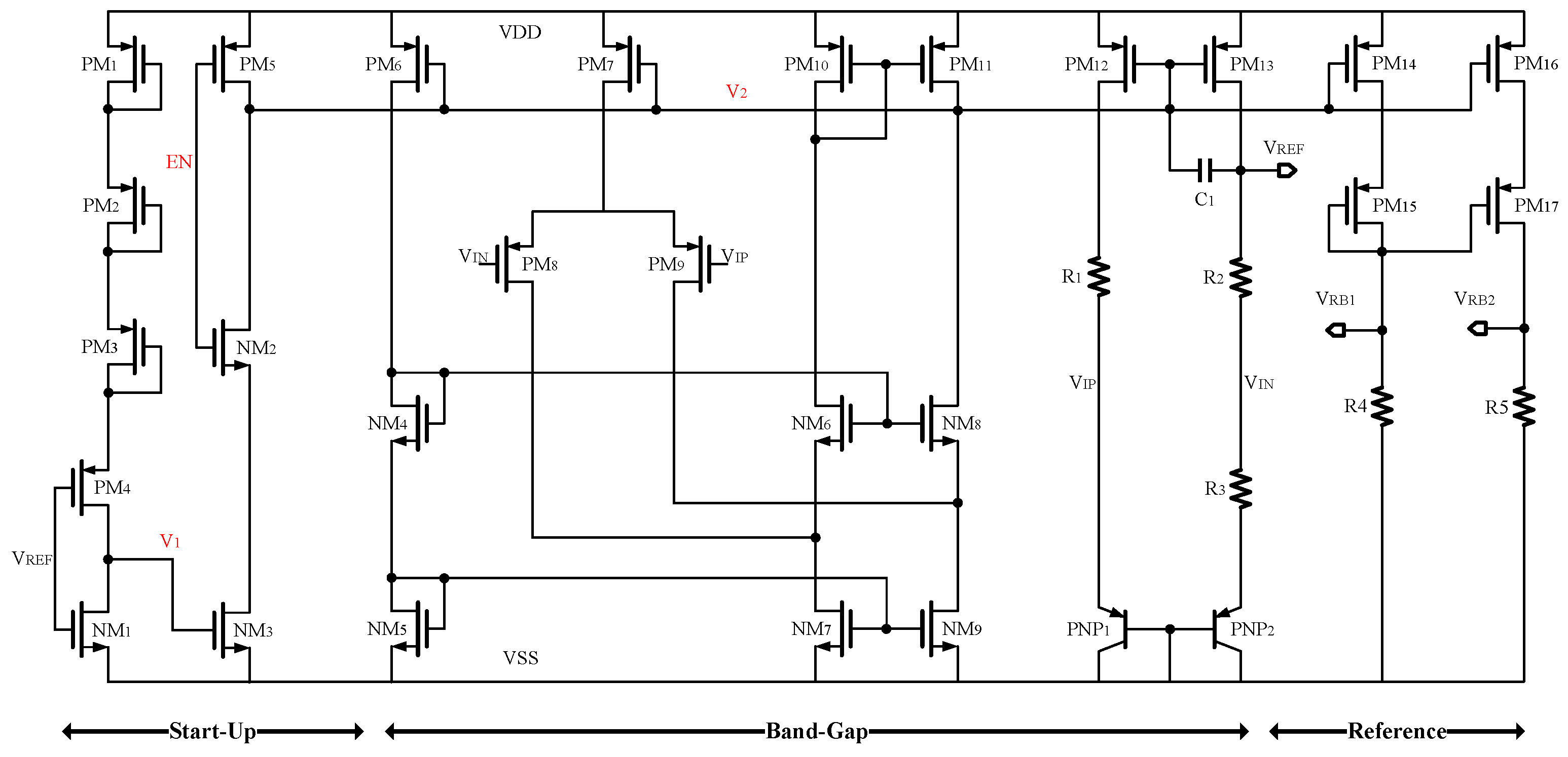
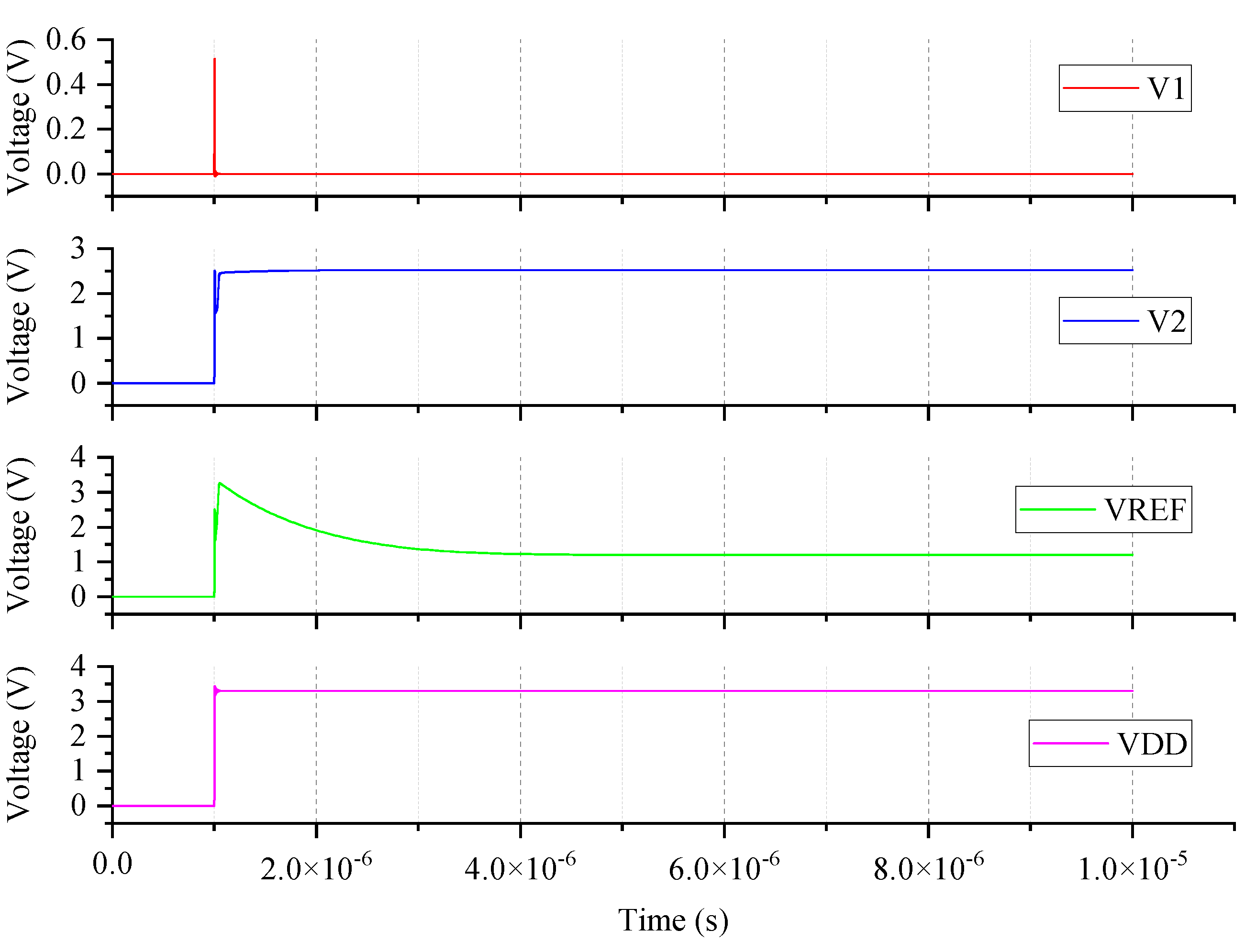
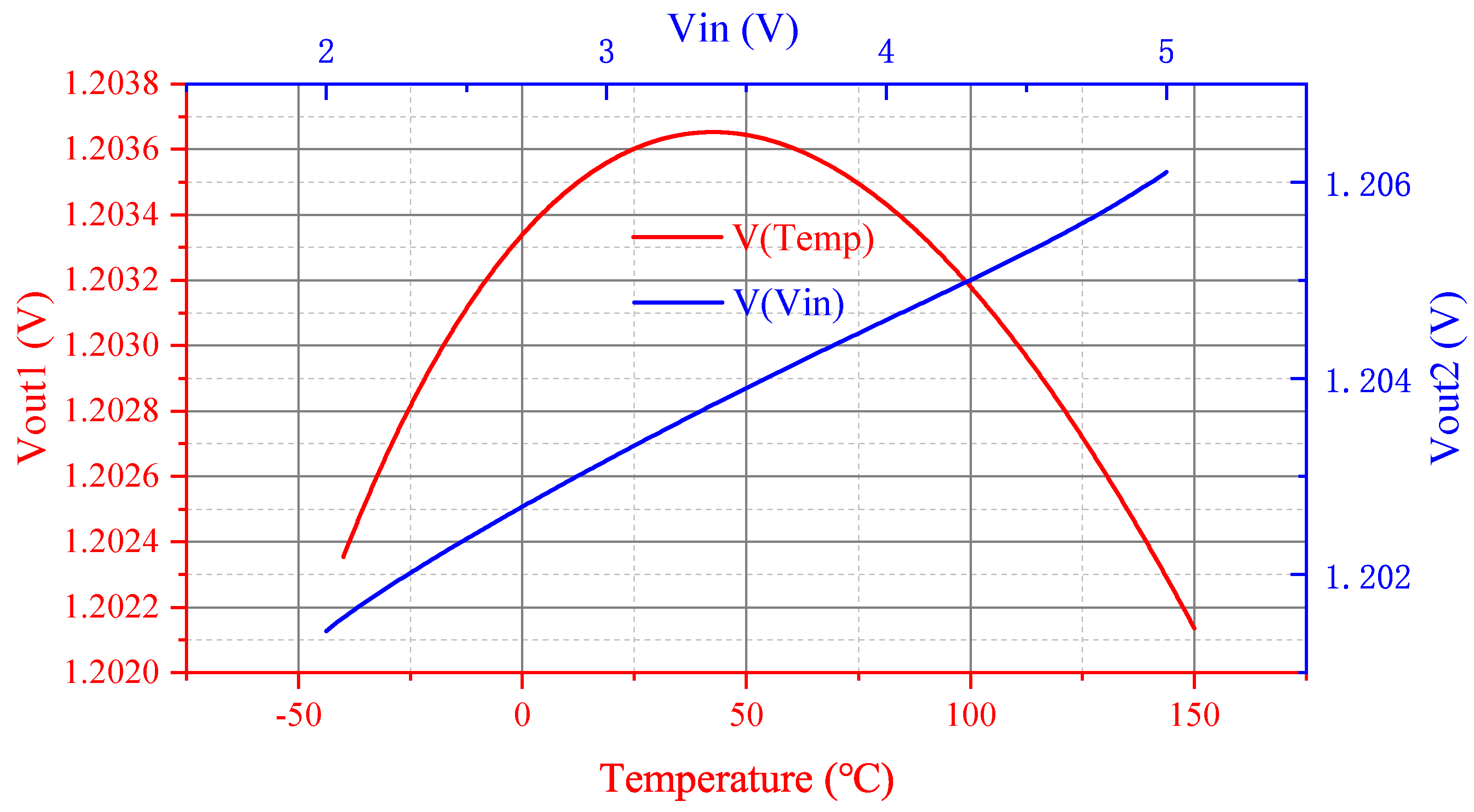
2.1. Reference Circuit

As shown in Figure 3, the reference circuit includes start up, band gap, and reference. The band-gap circuit is implemented with a conventional self-biasing circuit [23,24,25]. EN is the enable signal, which is mainly used to control the opening and closing of the band-gap reference circuit. When EN is VSS, the P M 5 tube is turned on and the N M 2 tube is turned off. The voltage of V 2 is pulled up to VDD, and then the entire band-gap reference circuit is turned off. When the EN signal is VDD, the P M 5 tube is turned off and the N M 2 tube is turned on. The Reference circuit operates normally. A start-up module is also added to the design of the reference circuit, which can accelerate the band-gap reference module to enter the normal working state and prevent the band-gap reference circuit from entering a deadlock state. When the power supply voltage is turned on, the voltage of V R E F is low. Because V R E F is low, the P M 4 tube is turned on and the N M 1 tube is turned off. The gate voltage V 1 of the N M 3 tube is pulled up by the P M 4 tube, and then the N M 3 tube is turned on. Because the EN signal is high at this time, the N M 2 tube is turned on. So, voltage V 2 is pulled low and the band-gap reference circuit starts working. When the output of the band-gap reference circuit is stable, the output voltage V R E F is about 1.2 V. The P M 4 tube is closed and the N M 1 tube is open. Voltage V 1 is pulled low, N M 3 is turned off, and then, the start-up circuit is turned off. Through the above analysis, it can be found that the start-up circuit is only operating at the initial moment. The simulation results of reference circuit are shown in Figure 4. According to the simulation results, it can be determined that the startup time of the entire reference circuit is 7.2 μ s.
In order to ensure that the currents of P M 12 and P M 13 are consistent, the resistor R1 is added. Figure 5 shows the simulation results of the reference circuit at different temperatures and voltages. According to Figure 5, we can know that the temperature coefficient of the band-gap reference circuit is 7.96 ppm/ C. When the input power supply voltage changes from 2 V to 5 V, the output voltage V R E F is 1.204 ± 0.002 V. In order to keep the voltage of V R B 1 and V R B 2 constant, R 4 and R 5 need to use resistors with negative temperature coefficients.
Taking into account the deviation made by the craft factory, Figure 6 shows the simulation results of the phase margin and gain at three different process angles where the three process angles are FF (−40 C), TT (27 C), and SS (80 C). According to the simulation results in Figure 6, it can be seen that under the three different process angles, the gain of the reference circuit is about 37 dB and the phase margin is greater than 60 degrees.

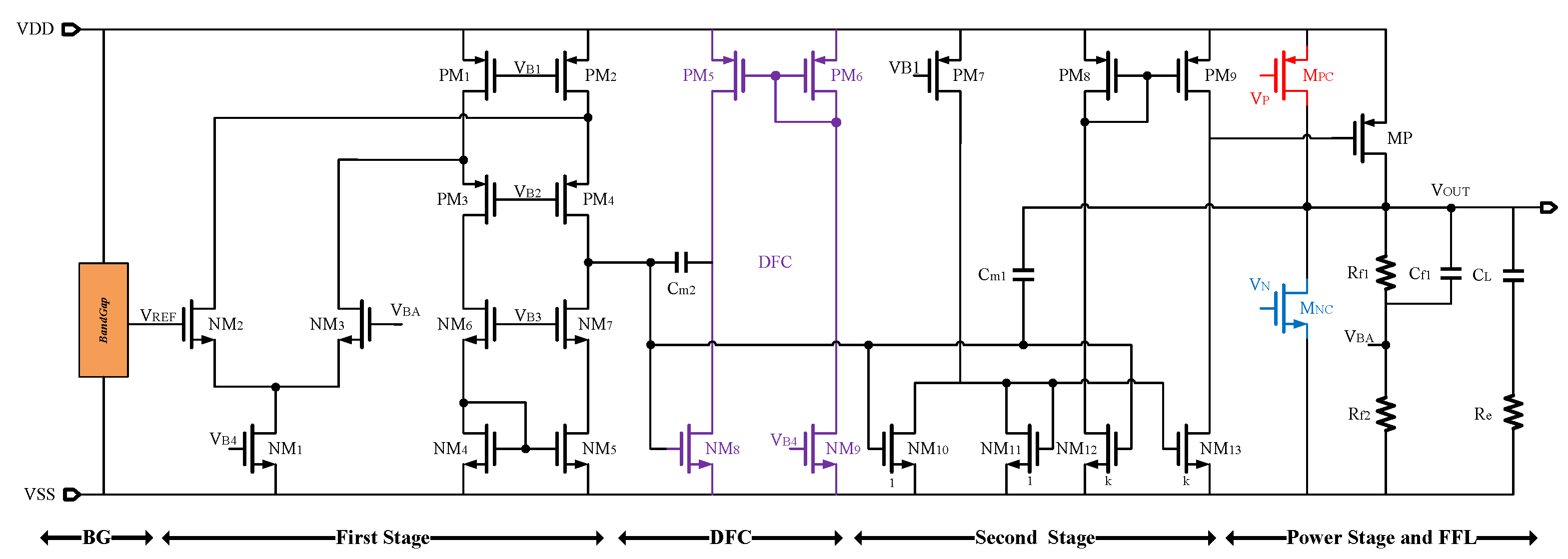
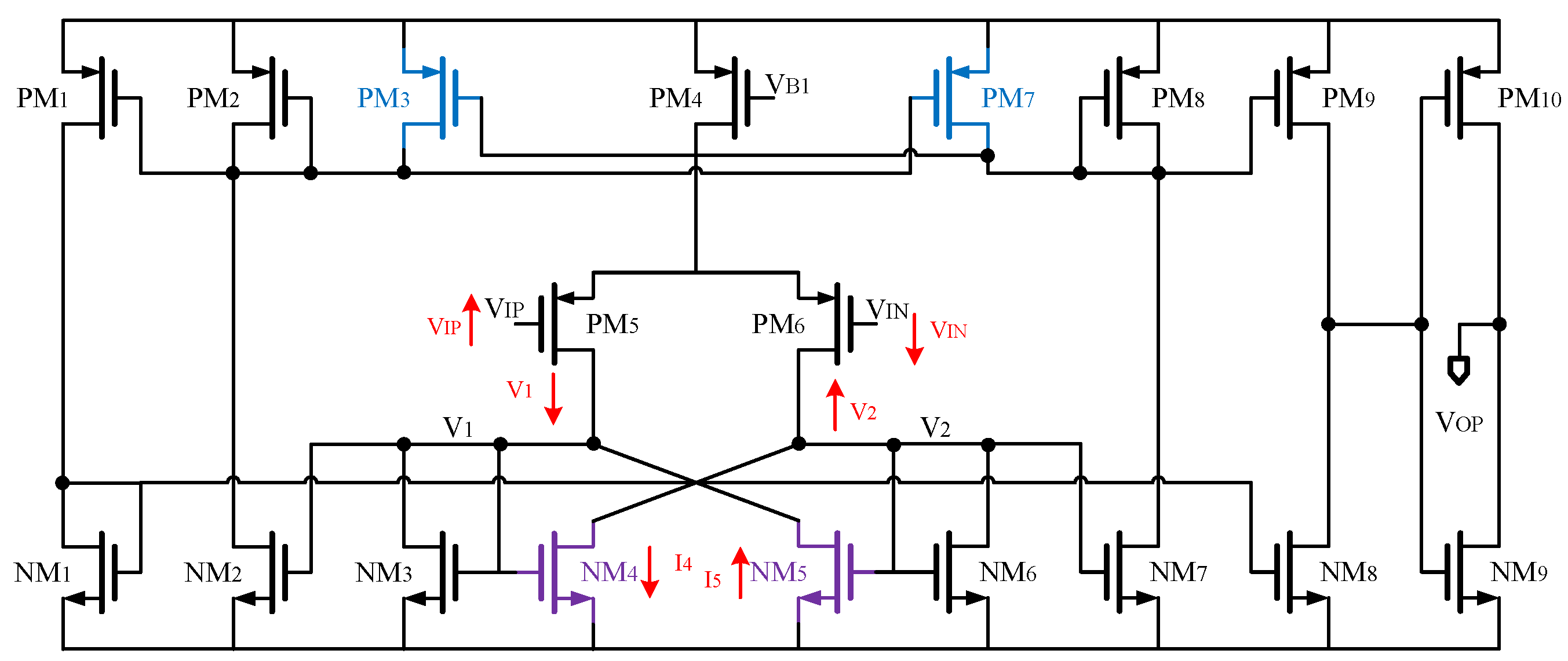
2.2. Error Amplifier and DFC

This OCL-LDO adopts a three-stage structure [26,27,28]. Figure 2 shows the circuit implementation of the proposed OCL-LDO. In the first stage, a folded cascode structure is used for high gain. In the second stage, the drain terminals of N M 10 and N M 11 are connected to the same current source, so the gate voltage of N M 11 will change opposite to the gate voltage of N M 10 . This voltage difference is translated into a 2k-times current difference through N M 12 and N M 13 . With this design, both the gain of the second stage and the driving ability can be improved. In this work, the value of k is 10, and the total gain of the OCL-LDO is 109 dB. C m 1 , C m 2 , C f 1 , and DFC are used to compensate the phase margin of the loop [29,30,31,32].

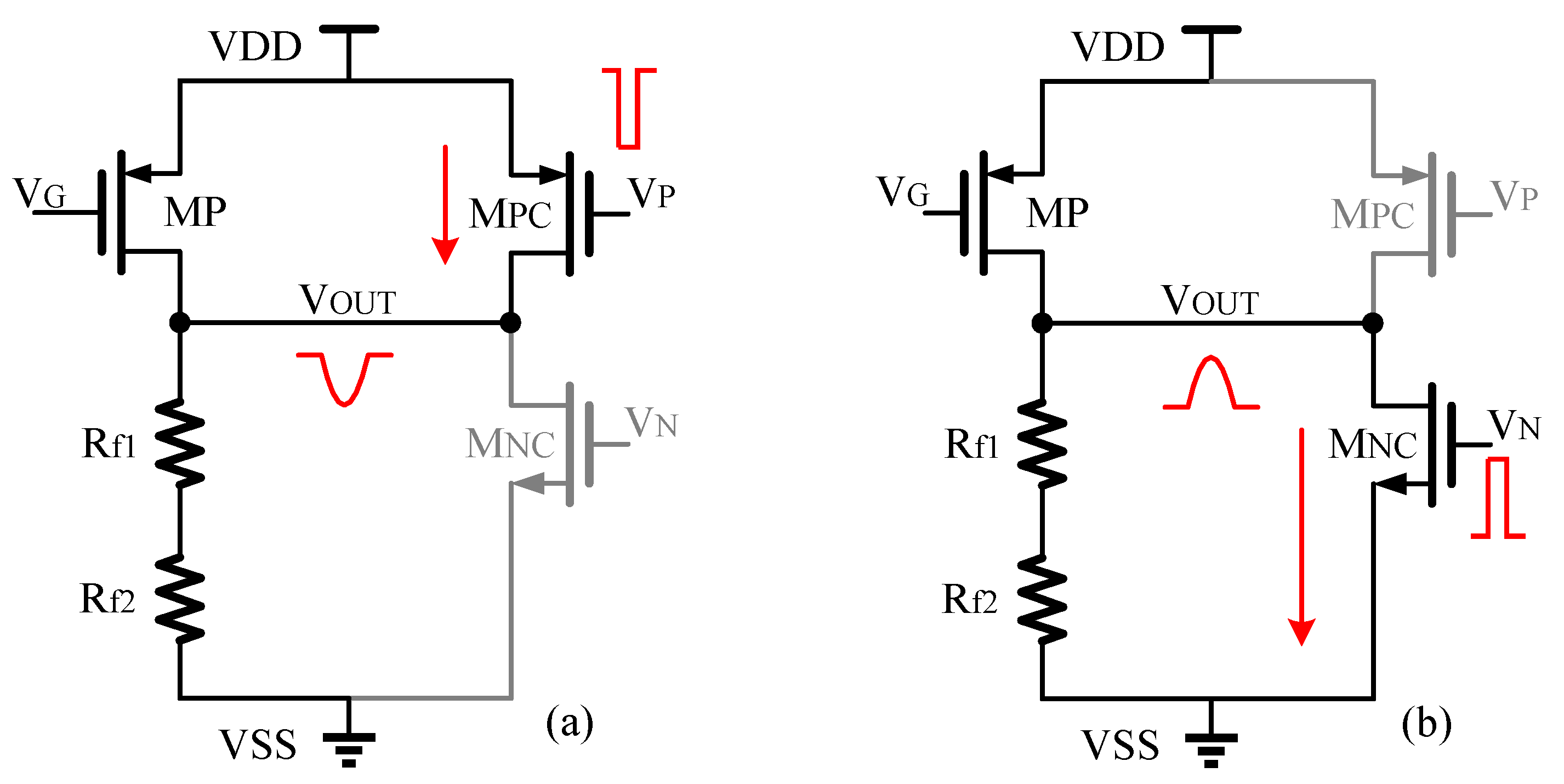
2.3. Fast Feedback Loop

As shown in Figure 1, when the output voltage is within the normal range, M N C and M P C are turned off. The following is an analysis of the working state of the FFL loop when the load current I L changes sharply. In Figure 7a, when the output voltage V O U T suddenly becomes low due to the load suddenly becoming high, the comparator controls M P C to turn on. Then, the output voltage V O U T is pulled up through the conduction of the M P C tube. In Figure 7b, when the output voltage V O U T suddenly becomes high due to the load suddenly becoming low, the comparator controls M N C to turn on. Then, the output voltage V O U T is pulled down through the conduction of the M N C tube. In order to improve the comparison speed of the comparator, this work proposes a comparator structure with positive feedback. The detailed circuit is shown in Figure 8. When V I P is greater than V I N , the voltage V 1 will become less than voltage V 2 . This also means that the gate voltage of N M 5 is greater than the gate voltage of N M 4 , so N M 5 will flow more charge than N M 4 .This results in a greater voltage difference between V 1 and V 2 than before. In short, N M 4 and N M 5 form a positive feedback structure. Likewise, P M 3 and P M 7 also form a positive feedback structure. These two positive feedback structures enable the comparator to obtain comparison results quickly. As can be seen from Figure 9, the comparison time of the comparator is 79 ns.

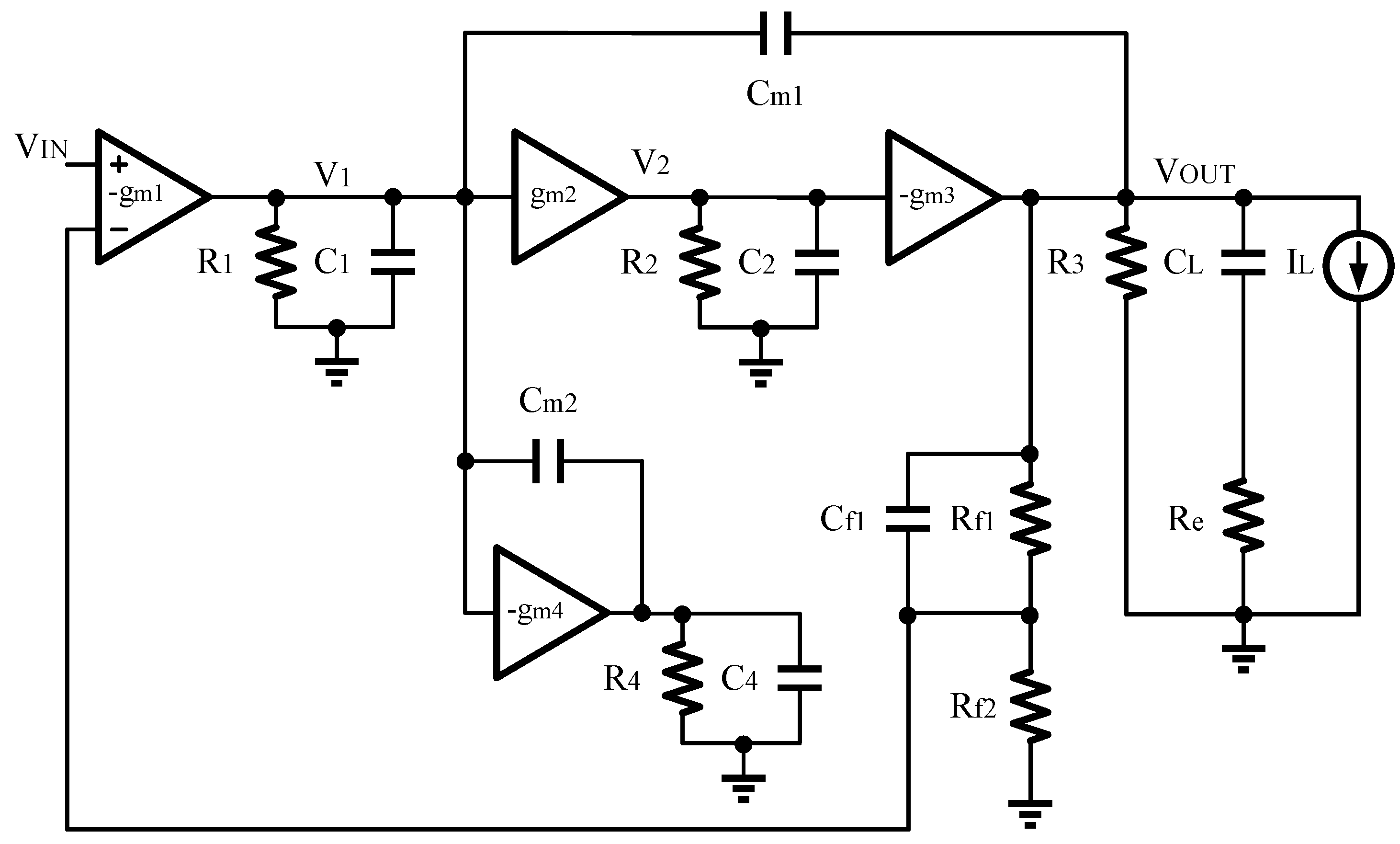
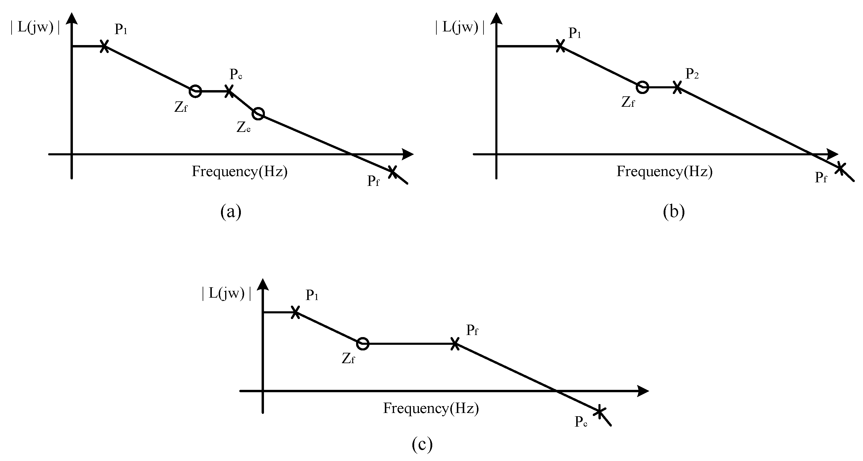
3. Frequency Compensation

Reference [10] has already mentioned that the DFC method can compensate the phase margin of the OCL-LDO. The DFC module designed in this work requires fewer tubes and reference voltages than reference [10]. The small-signal block diagram of the proposed OCL-LDO main circuit is given in Figure 10. According to the given small signal model, the loop gain of OCL-LDO under different load current and load capacitance is analyzed. When C L ≠ 0 and I L = 0, the loop gain is Equation (1). When C L ≠ 0 and I L ≠ 0, the loop gain is Equation (2). When C L = 0, the loop gain is Equation (3).
L O ( c a p ) ( s ) I L = 0 = L 0 ( 1 + s z e ) ( 1 + s z f ) ( 1 + s p 1 ) ( 1 + C L C p g m 4 C m 1 g m 2 g m 3 s + C p C L g m 2 g m 3 s 2 ) ( 1 + s p f ) = L 0 ( 1 + s z e ) ( 1 + s z f ) ( 1 + s p 1 ) ( 1 + 2 β p c s + ( 1 p c ) 2 s 2 ) ( 1 + s p f )
L O ( c a p ) ( s ) I L 0 = L 0 ( 1 + s z f ) ( 1 + s p 1 ) ( 1 + s p 2 ) ( 1 + s p f )
L O ( c a p f r e e ) ( s ) = L 0 ( 1 + s z f ) ( 1 + s p 1 ) ( 1 + s p f )
L O = ( R f 2 R f 1 + R f 2 ) g m 1 g m 2 g m 3 R 1 R 2 R 3
p 1 = 1 C m 1 g m 2 g m 3 R 1 R 2 R 3 , p 2 = g m 2 g m 3 R e C p p f = 1 C f 1 ( R f 1 / / R f 2 ) , z f = 1 C f 1 R f 1 , z e = 1 C L R e β = 1 2 C p C L g m 2 g m 3 ( g m 4 C m 1 ) , p c = g m 2 g m 3 C p C L
where C p is the gate capacitance of the power tube; g m 4 is the transconductance of the DFC; β is the damping factor; p c is the complex poles; L O is the loop gain of the proposed OCL-LDO; p 1 is the main pole; p 2 is the pole introduced by the power tube; z f and p f are the zero and pole points introduced by the DFC structure, respectively; g m 1 , g m 2 , g m 3 are the transconductances of the LDO; R 1 , R 2 , and R 3 are the output resistances of the LDO; C L is the output load capacitance; R e is the ESR resistance; and C m 1 , C m 2 , and C f 1 are the compensation capacitors.
According to Equation (1), when C L ≠ 0 and I L = 0, z f complements the main pole, z e complements a pole of p c , and the p f pole is designed outside the unity gain bandwidth. The specific zero-pole distribution is shown in Figure 11a. According to Equation (2), when C L ≠ 0 and I L ≠ 0, z f is used to compensate the main pole, and the p f pole is designed outside the unity gain bandwidth. The specific zero-pole distribution is shown in Figure 11b. According to Equation (3), when C L = 0, z f is used to compensate the dominant pole, the subdominant pole is p f , and the composite pole is located outside the unity gain bandwidth. The specific zero-pole distribution is shown in Figure 11c. It can be seen from the above analysis that OCL-LDO can maintain stability under different load capacitances. Figure 12 shows the simulation results when the load capacitance is 0 F. Figure 13 shows the simulation results when the load capacitance is 100 pF. Figure 14 shows the simulation results when the load capacitance is 1 μ F. It can be seen that stability is maintained under all load conditions. Furthermore, in all cases, the minimum phase margin of the loop is greater than 50 degrees.

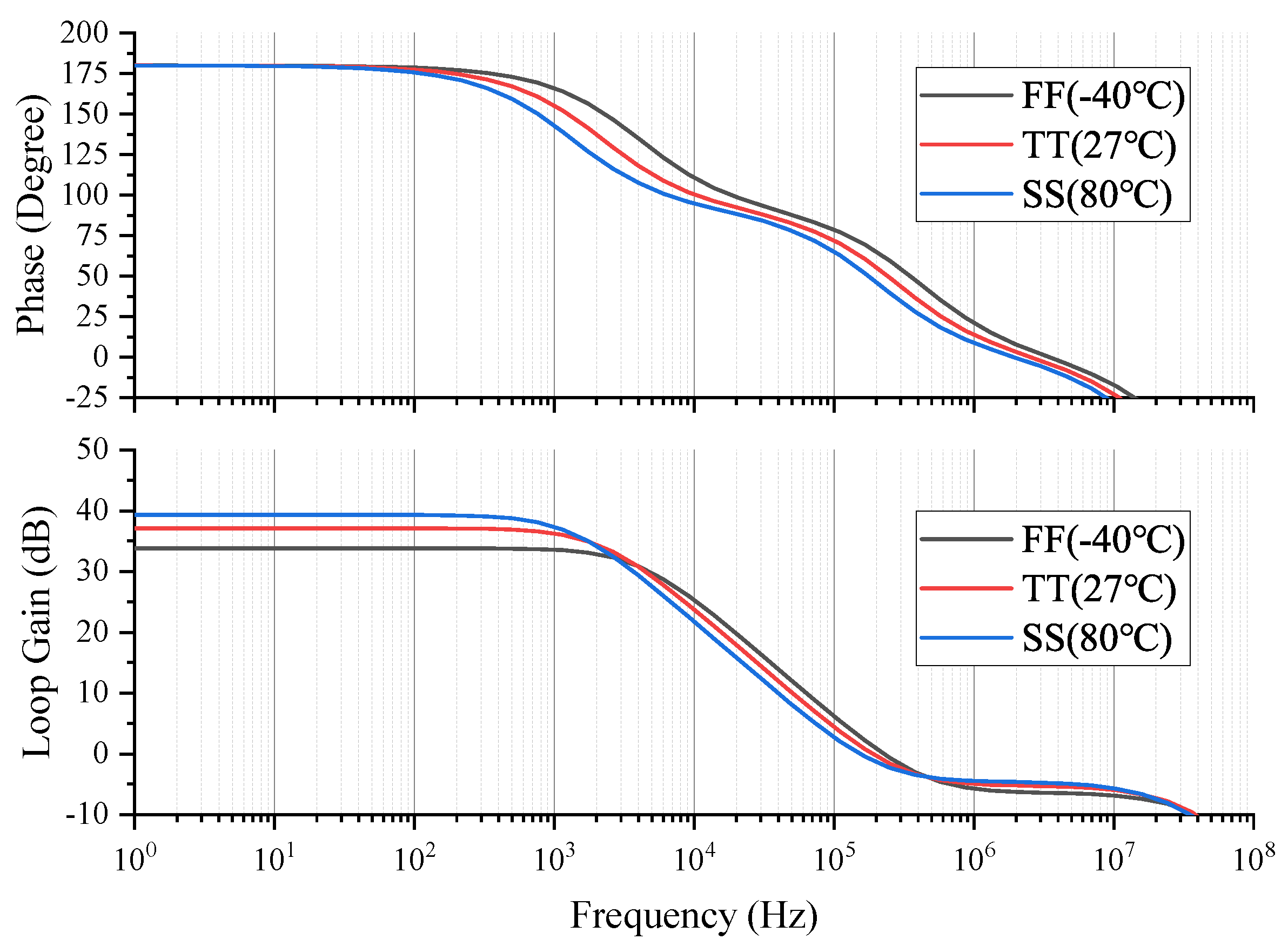
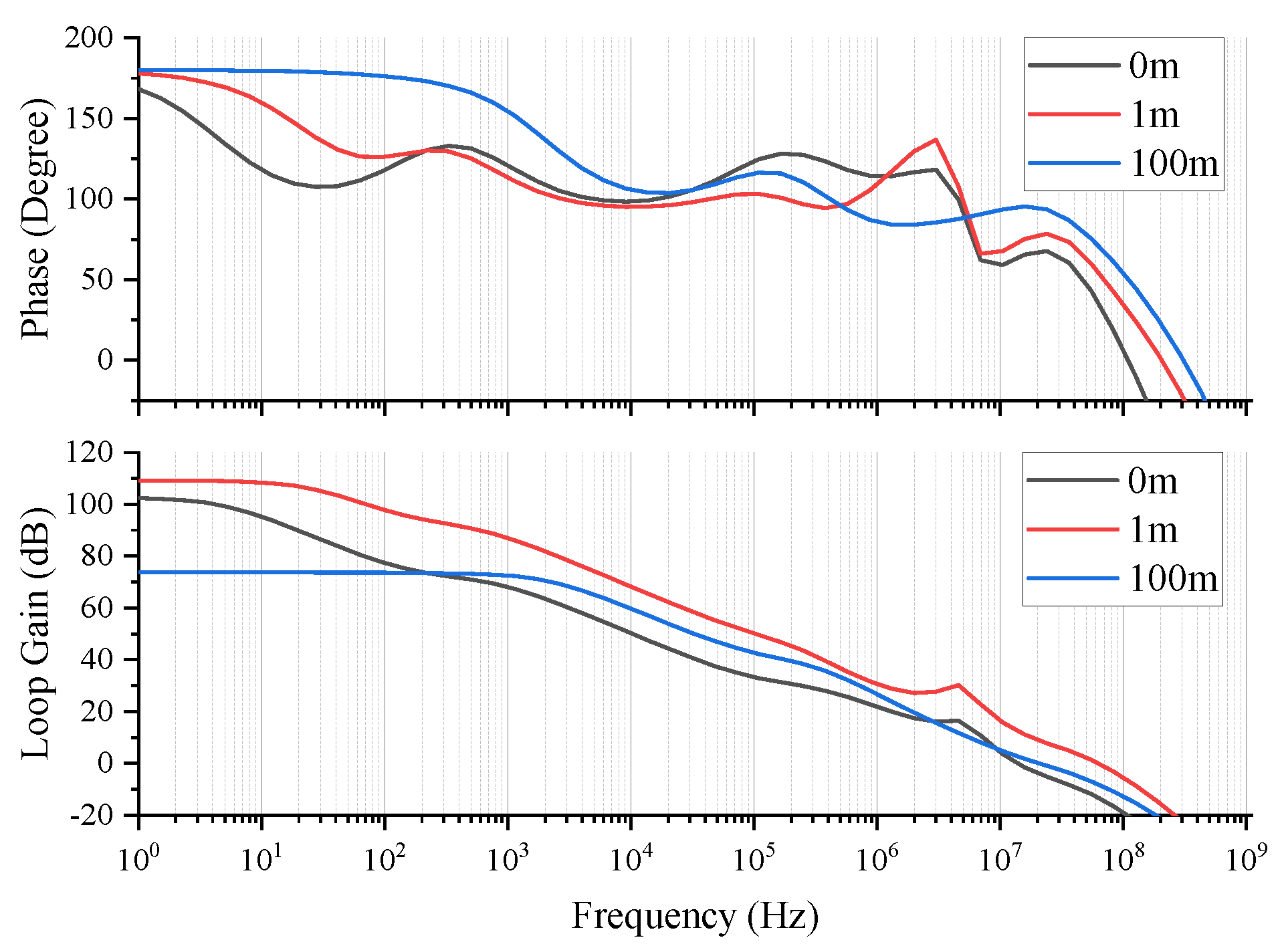
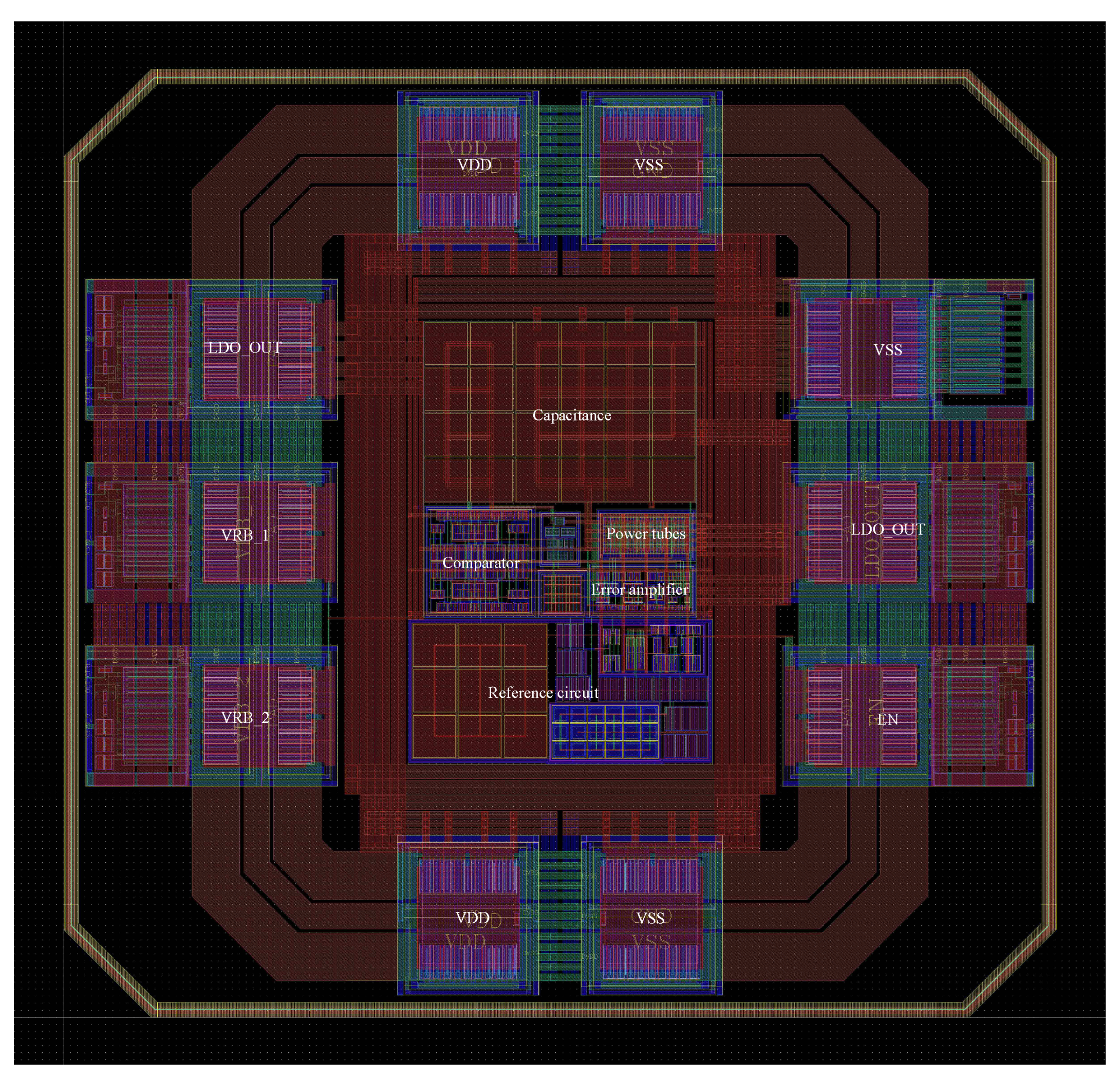
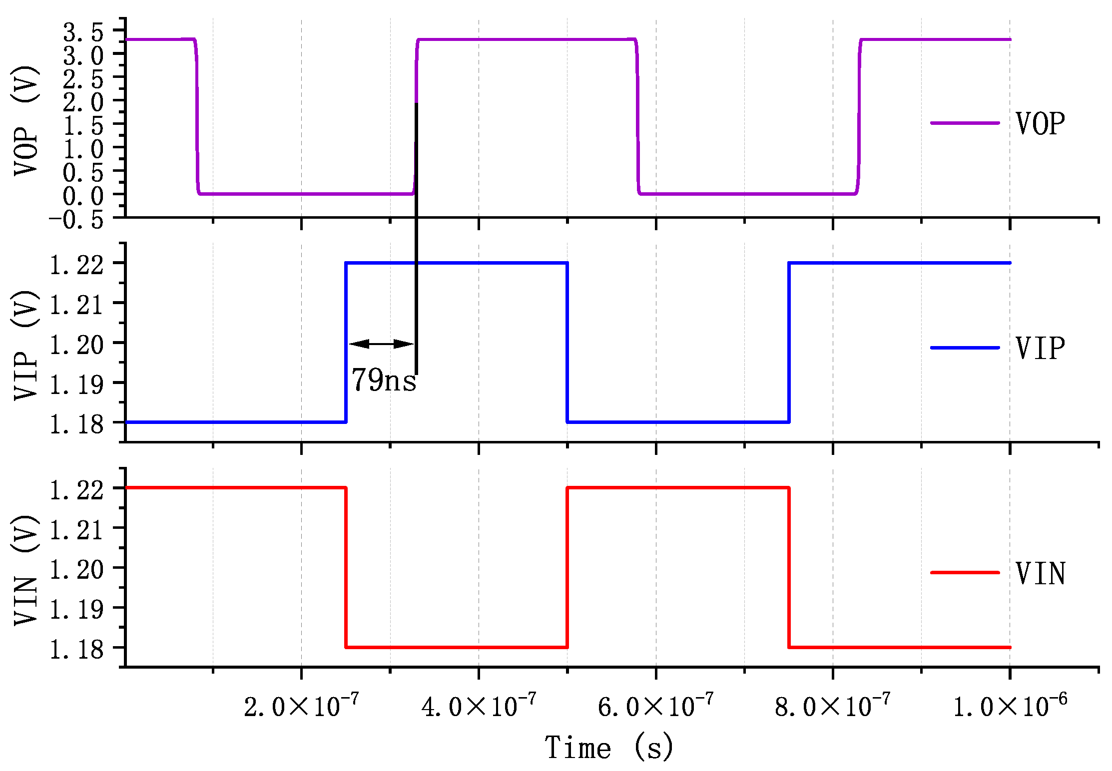
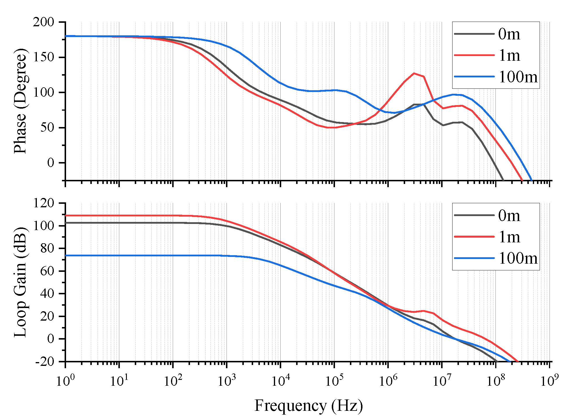
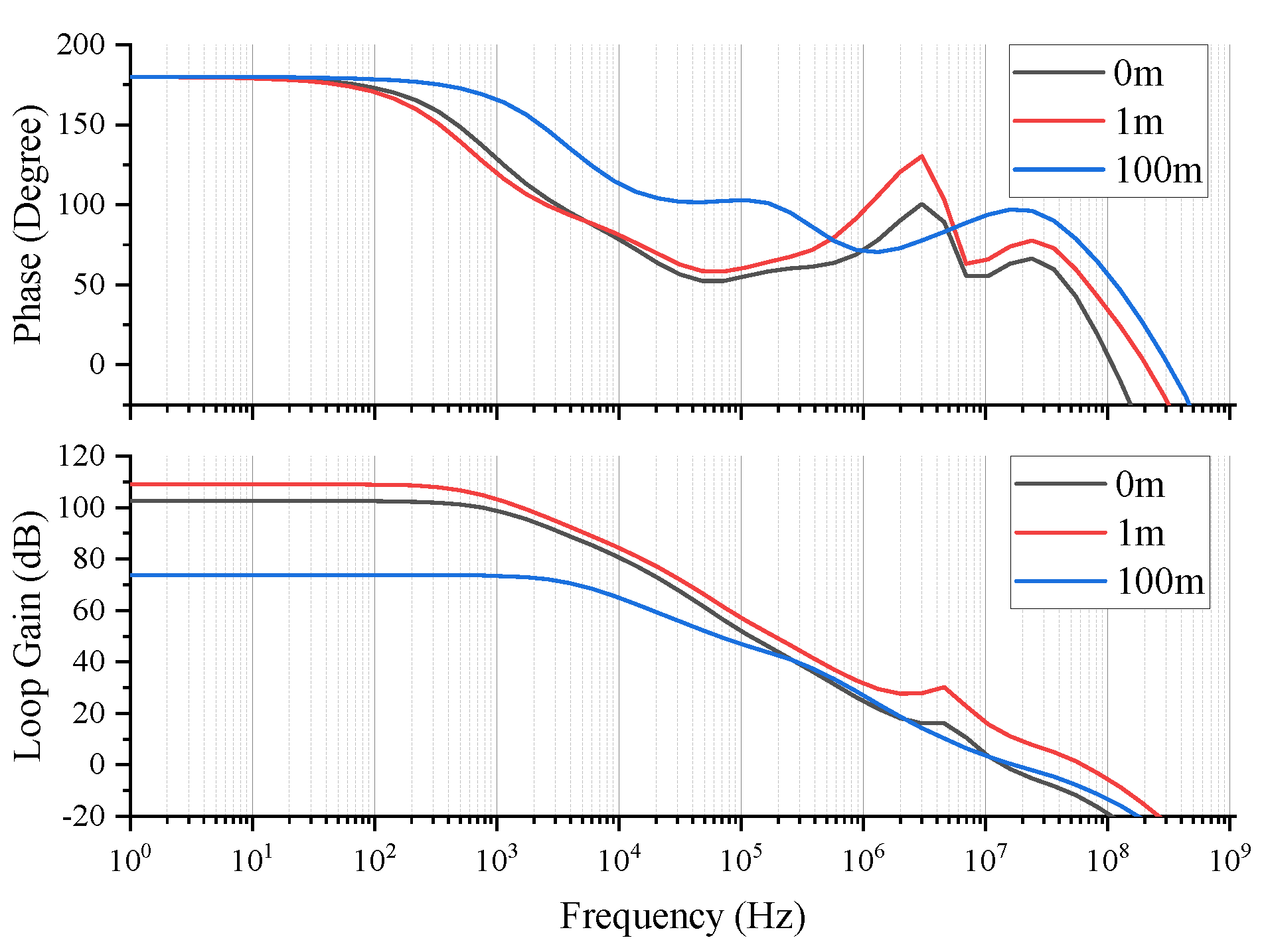
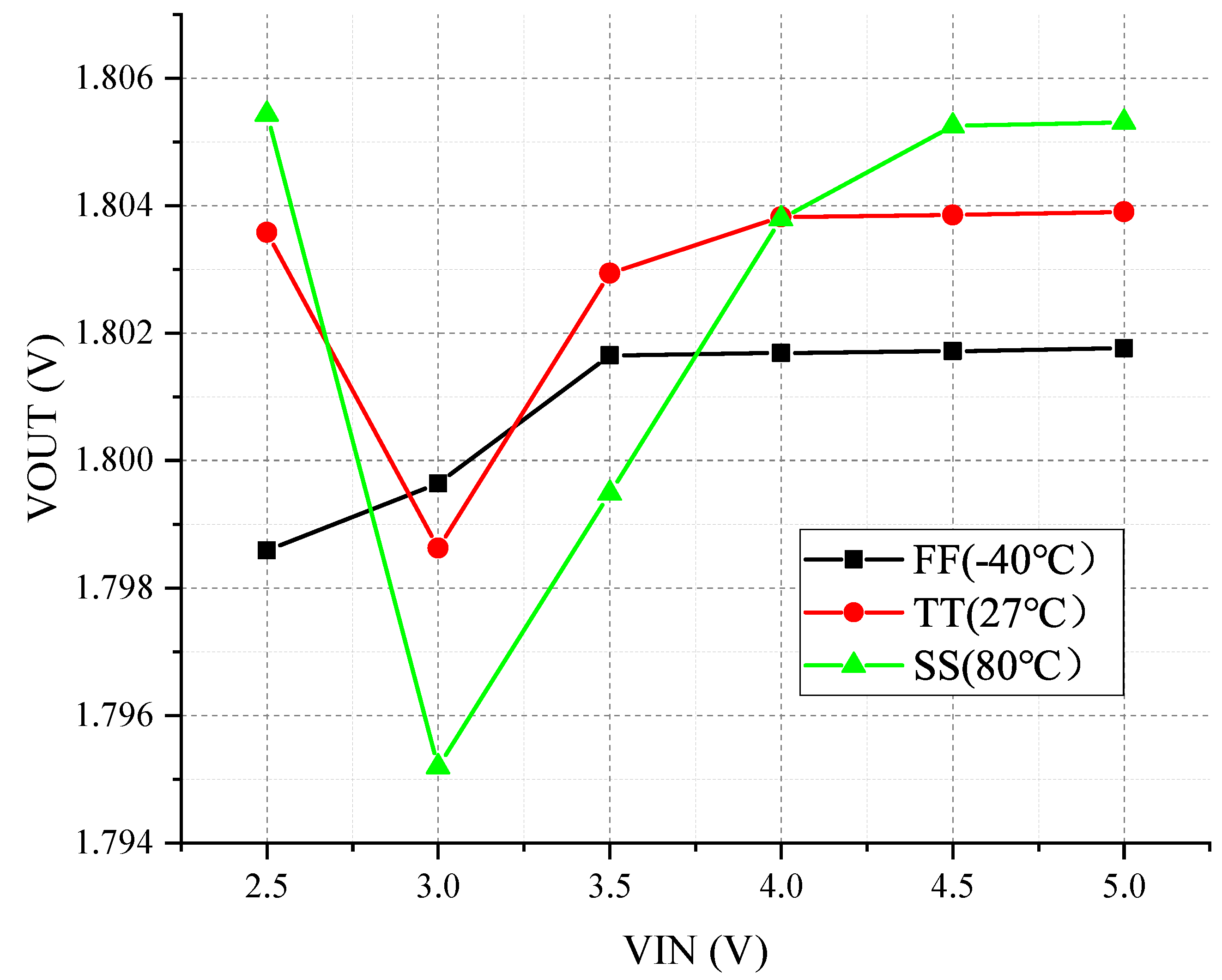
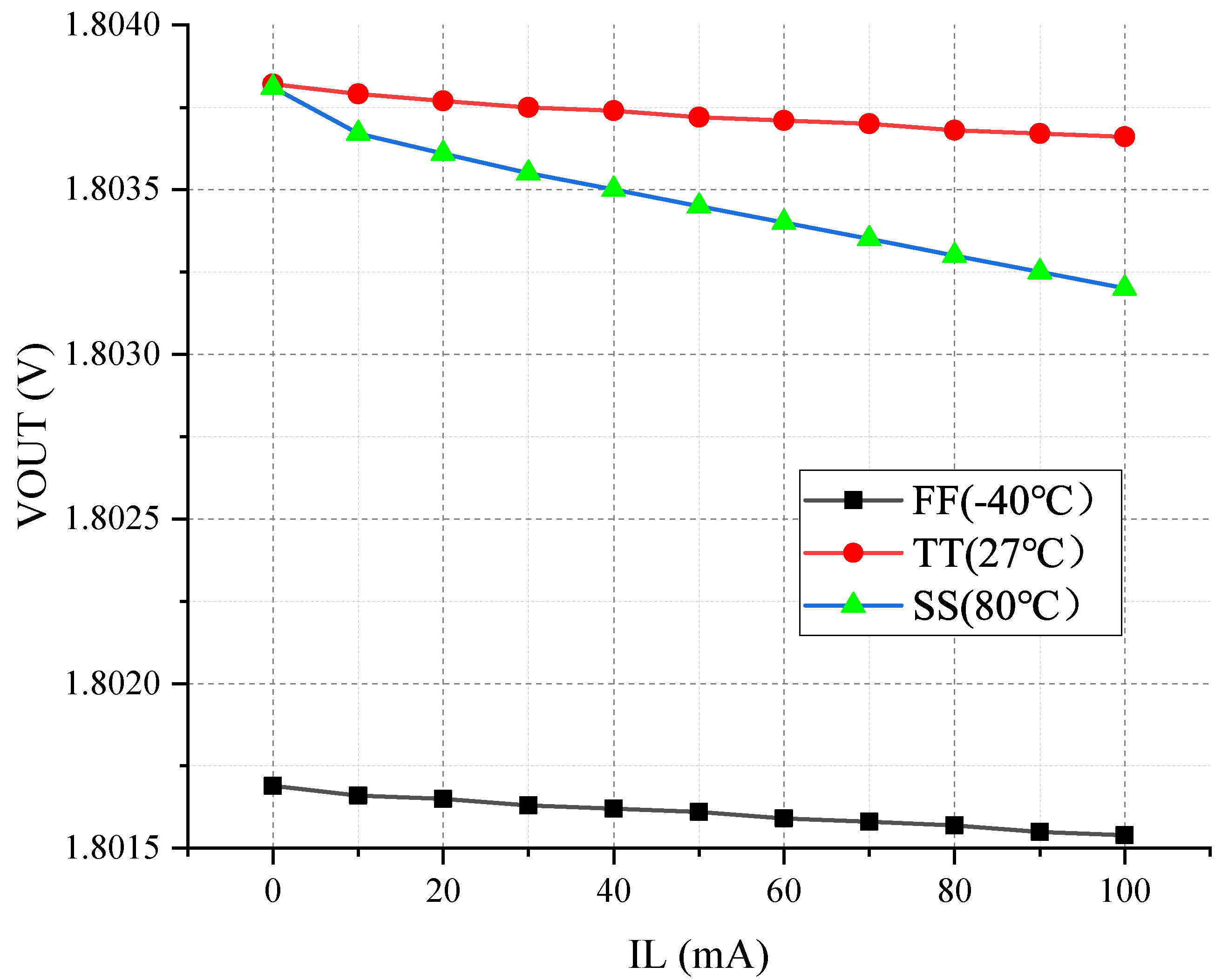
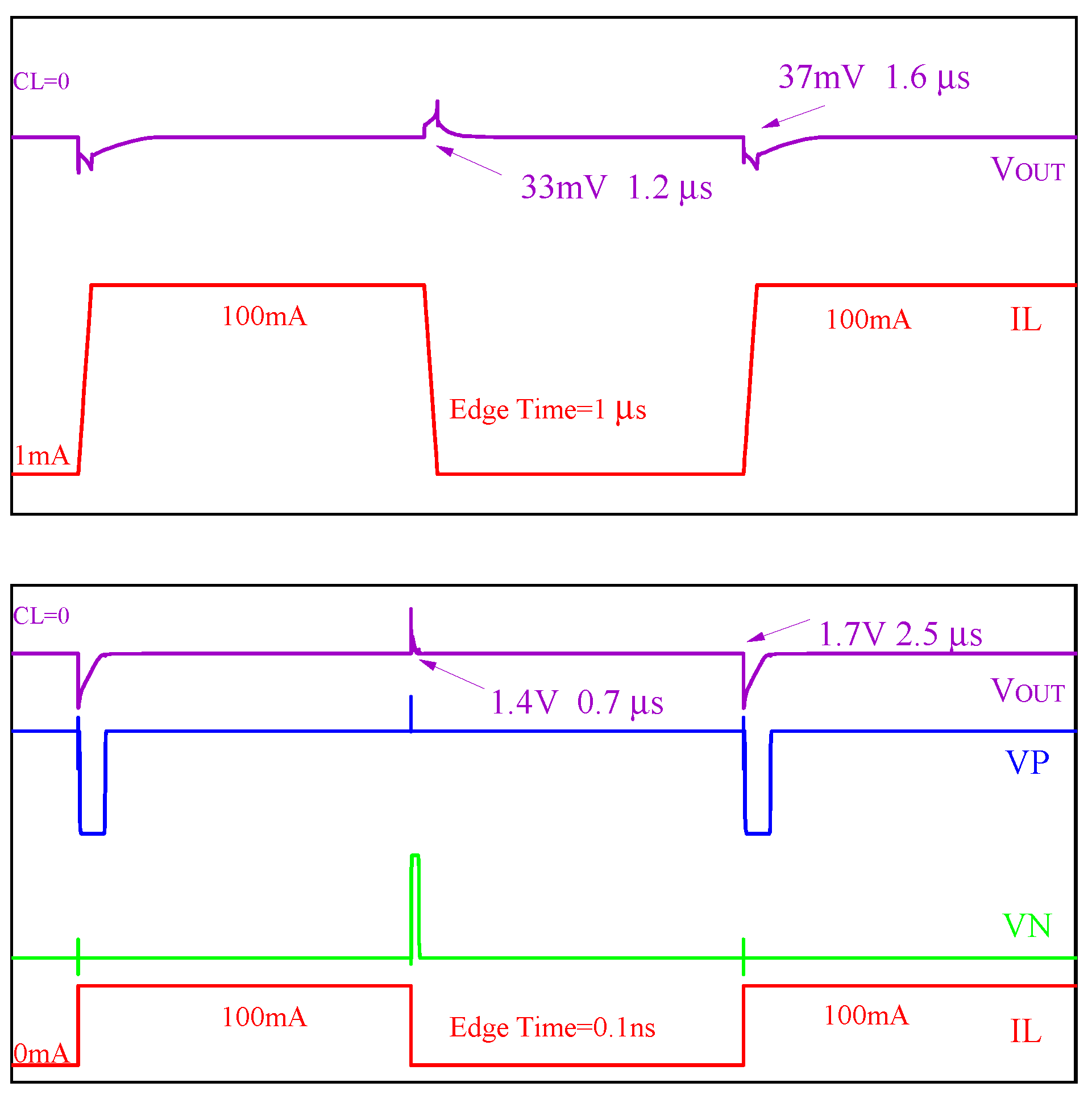
4. Simulation Results

Figure 15 shows the overall layout of the chip. The proposed OCL-LDO was implemented in 180 nm process with an active area of 216 μ m × 315 μ m (without pads). The power consumption of the whole chip is 136 μ A, and the power consumption of the OCL-LDO core is 76 μ A. The peak current efficiency achieved was 99.89%.
Figure 16 shows the line regulation rate of OCL-LDO. When the load is 1 mA and the input voltage V I N changes from 2.5 V to 5 V, the variation of output voltage is 0.32 mV. Therefore, the line regulation rate of OLC-LDO is 0.128 mV/V. Figure 17 shows the load regulation of OCL-LDO. When the load changes from 0 to 100 mA, the variation of output voltage is 0.17 mV. Therefore, the load regulation rate of OCL-LDO is 0.0017 mV/mA.
Figure 18 shows the measured load transient responses of the OCL-LDO regulator. When I L changes from 1 mA to 100 mA with an edge time of 1 μ s, the undershoot is 37 mV and the overshoot is 33 mV. The recovery time for the overshoot voltage is 1.2 μ s and the recovery time for the undershoot voltage is 1.6 μ s. When the output load I L changes from 0 to 100 mA with an edge time of 100 ps, the undershoot is 1.7 V and the overshoot is 1.4V. The recovery time for the overshoot voltage is 0.7 μ s, and the recovery time for the undershoot voltage is 2.5 μ s. It can be seen that when the load changes drastically, thanks to the proposed FFL fast feedback loop, the transient response time of the proposed OCL-LDO does not increase significantly. There is even smaller recovery time of the output overshoots.
A performance comparison between the proposed OCL-LDO regulator and other reported LDO regulators is shown in Table 1. Compared with others works, the proposed circuit is stable with or without a large external capacitor. Due to the high gain of the proposed OCL-LDO, its load regulation and line regulation are better than other works. Its gain is 109 dB, load regulation is 0.0017 mV/mA, and line regulation is 0.128 mV/V. The change of the output voltage of the proposed circuit is small, and its undershoot voltage and overshoot voltage are 37 mV and 33 mV, respectively, and the recovery time is 1.6 μ s. To compare various regulators implemented in different technologies, a comparison method based on FOM is adopted. Its calculation method is Equation (4) [6,12].
F O M = K ( Δ V O U T C T × I Q Δ I O U T 2 )
where K is the edge time ratio and is defined as:
K = Δ t u s e d i n t h e m e a s u r e m e n t t h e s m a l l e s t Δ t a m o n g t h e d e s i g n s f o r c o m p a r i s o n
From Table 1, the proposed OCL-LDO regulator design achieves a comparable or better FOM with the other reported LDO regulators.

5. Conclusions

OCL-LDOs are attracting more and more attention because of their convenience for integration with other circuit modules. However, OCL-LDOs usually have poor transient characteristics. This work proposes a comparator-based transient enhanced OCL-LDO. Due to the fast response speed of the comparator, the transient characteristics of the OCL-LDO can be greatly improved. The overshoot and undershoot voltages of the proposed OCL-LDO are 33 mV and 37 mV, respectively, and the recovery time are 1.2 μ s and 1.6 μ s, respectively. Through the DFC frequency compensation technology, it can be ensured that the output of the OCL-LDO remains stable within the load variation range of 0 mA to 100 mA. The phase margin of the proposed OCL-LDO can be greater than 50 degrees under different current loads and capacitive loads. The proposed OCL-LDO integrates a band-gap reference, which can make its output temperature invariant and more reliable for integration with other modules.

Author Contributions

Conceptualization, Y.N., J.G. and G.G.; methodology, Y.N.; validation, J.G. and G.G.; formal analysis, Y.N. and D.L.; investigation, Y.N. and Y.J.; data curation, Y.N. and D.L; writing—original draft preparation, Y.N.; writing—review and editing, Y.N. and G.G.; project administration, G.G. All authors have read and agreed to the published version of the manuscript.

Funding

This research received no external funding.

Data Availability Statement

No new data were created or analyzed in this study. Data sharing is not applicable to this paper.

Conflicts of Interest

The authors declare no conflict of interest.

References

  1. Chong, S.; Chan, P.K. A 0.9-/spl mu/A Quiescent Current Output-Capacitorless LDO Regulator with Adaptive Power Transistors in 65-nm CMOS. IEEE Trans. Circuits Syst. I Regul. Pap. 2013, 60, 1072–1081. [Google Scholar] [CrossRef]
  2. Desai, C.; Mandal, D.; Bakkaloglu, B.; Kiaei, S. A 1.66 mV FOM Output Cap-Less LDO with Current-Reused Dynamic Biasing and 20 ns Settling Time. IEEE Solid-State Circuits Lett. 2018, 1, 50–53. [Google Scholar] [CrossRef]
  3. Guo, J.; Leung, K.N. A 6-μ W Chip-Area-Efficient Output-Capacitorless LDO in 90-nm CMOS Technology. IEEE J. Solid-State Circuits 2010, 45, 1896–1905. [Google Scholar] [CrossRef]
  4. Kim, Y.i.; Lee, S.S. A Capacitorless LDO Regulator with Fast Feedback Technique and Low-Quiescent Current Error Amplifier. IEEE Trans. Circuits Syst. II Express Briefs 2013, 60, 326–330. [Google Scholar] [CrossRef]
  5. Han, W.; Lee, H. A 340-nA-Quiescent 80-mA-Load 0.02-fs-FOM Active-Capacitor-Based Low-Dropout Regulator in Standard 0.18-μm CMOS. IEEE Solid-State Circuits Lett. 2021, 4, 125–128. [Google Scholar] [CrossRef]
  6. Mandal, D.; Desai, C.; Bakkaloglu, B.; Kiaei, S. Adaptively Biased Output Cap-Less NMOS LDO with 19 ns Settling Time. IEEE Trans. Circuits Syst. II Express Briefs 2019, 66, 167–171. [Google Scholar] [CrossRef]
  7. Jiang, Y.; Wang, L.; Wang, S.; Cui, M.; Zheng, Z.; Li, Y. A Low-Power, Fast-Transient Output-Capacitorless LDO with Transient Enhancement Unit and Current Booster. Electronics 2022, 11, 701. [Google Scholar] [CrossRef]
  8. Limpisawas, T.; Wattanapanitch, W. A Low-Power Wide-Load-Range Output-Capacitorless Low-Dropout Voltage Regulator with Indirect-Direct Nested Miller Compensation. IEEE Access 2022, 10, 67396–67412. [Google Scholar] [CrossRef]
  9. Shen, L.; Yan, Z.; Zhang, X.; Zhao, Y.; Wang, Y. Design of High-Performance Voltage Regulators Based on Frequency-Dependent Feedback Factor. In Proceedings of the 2007 IEEE International Symposium on Circuits and Systems (ISCAS), New Orleans, LA, USA, 27–30 May 2007; pp. 3828–3831. [Google Scholar] [CrossRef]
  10. Leung, K.N.; Mok, P. A capacitor-free CMOS low-dropout regulator with damping-factor-control frequency compensation. IEEE J. Solid-State Circuits 2003, 38, 1691–1702. [Google Scholar] [CrossRef]
  11. Tan, X.L.; Chong, S.S.; Chan, P.K.; Dasgupta, U. A LDO Regulator with Weighted Current Feedback Technique for 0.47 nF–10 nF Capacitive Load. IEEE J. Solid-State Circuits 2014, 49, 2658–2672. [Google Scholar] [CrossRef]
  12. Ho, E.N.Y.; Mok, P.K.T. A Capacitor-Less CMOS Active Feedback Low-Dropout Regulator with Slew-Rate Enhancement for Portable On-Chip Application. IEEE Trans. Circuits Syst. II Express Briefs 2010, 57, 80–84. [Google Scholar] [CrossRef]
  13. Leung, K.N.; Mok, P.; Ki, W.H.; Sin, J. Three-stage large capacitive load amplifier with damping-factor-control frequency compensation. IEEE J. Solid-State Circuits 2000, 35, 221–230. [Google Scholar] [CrossRef]
  14. Leung, K.N.; Mok, P. Analysis of multistage amplifier-frequency compensation. IEEE Trans. Circuits Syst. I Fundam. Theory Appl. 2001, 48, 1041–1056. [Google Scholar] [CrossRef]
  15. Liang, Y.; Diao, S. A Capacitor-Free Low-Dropout Regulator with Low Line Regulation Rate and High Stability. In Proceedings of the 2021 14th International Congress on Image and Signal Processing, BioMedical Engineering and Informatics (CISP-BMEI), Shanghai, China, 23–25 October 2021; pp. 1–5. [Google Scholar] [CrossRef]
  16. Li, G.; Qian, H.; Guo, J.; Mo, B.; Lu, Y.; Chen, D. Dual Active-Feedback Frequency Compensation for Output-Capacitorless LDO with Transient and Stability Enhancement in 65-nm CMOS. IEEE Trans. Power Electron. 2020, 35, 415–429. [Google Scholar] [CrossRef]
  17. Gao, M.; Cai, X.; Yan, W.; Zhao, H.; Xia, R.; Gao, Y. A wide input range, external capacitor-less LDO with fast transient response. IEICE Electron. Express 2023, 20, 20230008. [Google Scholar] [CrossRef]
  18. Lee, Y.S.; Im, Y.C.; Lee, H.; Kim, Y.S. Capless Low-Dropout Regulator with a Dual Feedback Loop and Voltage Dampers. In Proceedings of the 2022 19th International SoC Design Conference (ISOCC), Gangneung-si, Republic of Korea, 19–22 October 2022; pp. 298–299. [Google Scholar] [CrossRef]
  19. Wook, K.S.; Koo, Y.S. Design of high-reliability LDO regulator with SCR based ESD protection circuit using body technique and load transient detection. IEICE Electron. Express 2022, 19, 20220110. [Google Scholar] [CrossRef]
  20. Hicham, A.; Qjidaa, H. A 500μA low drop-out voltage regulator in 90-nm CMOS technology. In Proceedings of the 2012 IEEE International Conference on Complex Systems (ICCS), Agadir, Morocco, 5–6 November 2012; pp. 1–4. [Google Scholar] [CrossRef]
  21. Chen, C.M.; Hung, C.C. A capacitor-free CMOS low-dropout voltage regulator. In Proceedings of the 2009 IEEE International Symposium on Circuits and Systems, Taipei, Taiwan, 24–27 May 2009; pp. 2525–2528. [Google Scholar] [CrossRef]
  22. Abbasi, M.U.; Bagnall, D.; Bn, V. A high PSRR capacitor-less on—Chip low dropout voltage regulator. In Proceedings of the IEEE 8th International Symposium on Intelligent Systems and Informatics, Subotica, Serbia, 10–11 September 2010; pp. 361–364. [Google Scholar] [CrossRef]
  23. Hsiao, S.W.; Huang, Y.C.; Liang, D.; Chen, H.W.; Chen, H.S. A 1.5-V 10-ppm//spl deg/C 2nd-order curvature-compensated CMOS bandgap reference with trimming. In Proceedings of the 2006 IEEE International Symposium on Circuits and Systems (ISCAS), Kos, Greece, 21–24 May 2006; pp. 565–568. [Google Scholar] [CrossRef]
  24. Perry, R.T.; Lewis, S.H.; Brokaw, A.P.; Viswanathan, T.R. A 1.4 V Supply CMOS Fractional Bandgap Reference. IEEE J. Solid-State Circuits 2007, 42, 2180–2186. [Google Scholar] [CrossRef]
  25. Leung, K.N.; Mok, P. A sub-1-V 15-ppm//spl deg/C CMOS bandgap voltage reference without requiring low threshold voltage device. IEEE J. Solid-State Circuits 2002, 37, 526–530. [Google Scholar] [CrossRef]
  26. Ni, S.; Chen, Z.; Hu, C.; Chen, H.; Wang, Q.; Li, X.; Song, S.; Song, Z. An Output-Capacitorless Low-Dropout Regulator with Slew-Rate Enhancement. Micromachines 2022, 13, 1594. [Google Scholar] [CrossRef]
  27. Guo, Z.; Li, H.; Li, D.; Fan, S.; Gui, X.; Xue, Z.; Chen, Z.; Geng, L. Topological Classification-Based Splitting–Combining Methodology for Analysis of Complex Multi-Loop Systems and Its Application in LDOs. IEEE Trans. Power Electron. 2019, 34, 7025–7039. [Google Scholar] [CrossRef]
  28. Kao, S.K.; Chen, J.J.; Liao, C.H. A Multipath Output-Capacitor-Less LDO Regulator. IEEE Access 2022, 10, 27185–27196. [Google Scholar] [CrossRef]
  29. Giustolisi, G.; Palumbo, G.; Spitale, E. Robust Miller Compensation with Current Amplifiers Applied to LDO Voltage Regulators. IEEE Trans. Circuits Syst. I Regul. Pap. 2012, 59, 1880–1893. [Google Scholar] [CrossRef]
  30. Ming, X.; Kuang, J.J.; Gong, X.C.; Lin, Z.; Xiong, J.; Qin, Y.; Wang, Z.; Zhang, B. A Fast-Transient Capacitorless LDO with Dual Paths Active-Frequency Compensation Scheme. IEEE Trans. Power Electron. 2022, 37, 10332–10347. [Google Scholar] [CrossRef]
  31. Sakolski, O.; Poongodan, P.K.; Vanselow, F.; Maurer, L. A Feedforward Compensated High-Voltage Linear Regulator with Fast Response, High-Current Sinking Capability. IEEE Solid-State Circuits Lett. 2020, 3, 114–117. [Google Scholar] [CrossRef]
  32. Lu, Y.; Chen, M.; Wang, K.; Yang, Y.; Wang, H. A Capacitorless Flipped Voltage Follower LDO with Fast Transient Using Dynamic Bias. Electronics 2022, 11, 3009. [Google Scholar] [CrossRef]
Figure 1. The proposed OCL-LDO regulator.
Electronics 12 04067 g001
Figure 2. Proposed OCL-LDO with DFC.
Electronics 12 04067 g002
Figure 3. Reference circuit.
Electronics 12 04067 g003
Figure 4. Transient simulation results of the reference circuit.
Electronics 12 04067 g004
Figure 5. Simulation results of the reference circuit at different temperatures.
Electronics 12 04067 g005
Figure 6. Gain and phase margin of reference circuit under different process angles.
Electronics 12 04067 g006
Figure 7. Response of the FFL loop when the output changes. (a) Load current I L suddenly becomes larger, (b) Load current I L suddenly becomes smaller.
Electronics 12 04067 g007
Figure 8. Comparator schematic.
Electronics 12 04067 g008
Figure 9. Comparator simulation results.
Electronics 12 04067 g009
Figure 10. Small-signal model of the proposed OCL-LDO.
Electronics 12 04067 g010
Figure 11. Distribution of zeros and poles at different load capacitances and load currents. (a): C L ≠ 0 and I L = 0, (b): C L ≠ 0 and I L ≠ 0, (c): C L = 0.
Electronics 12 04067 g011
Figure 12. Stability simulation results ( C L = 0 F).
Electronics 12 04067 g012
Figure 13. Stability simulation results ( C L = 100 pF).
Electronics 12 04067 g013
Figure 14. Stability simulation results ( C L = 1 μ F).
Electronics 12 04067 g014
Figure 15. Layout of the chip.
Electronics 12 04067 g015
Figure 16. Line regulation rate of OCL-LDO.
Electronics 12 04067 g016
Figure 17. Load regulation of OCL-LDO.
Electronics 12 04067 g017
Figure 18. Transient responses of the OCL-LDO.
Electronics 12 04067 g018
Table 1. Comparison with some advanced LDOs.
Reference[30][17][11][31][29][27]This Work
Year2022202320142020201220192023
Technology (nm)35050065180350180180
Chip size (mm 2 )0.0770.290.0130.150.40.180.068
V IN (V)2.7∼3.35.2–200.75∼1.2701.2∼1.53.32.5–5
V OUT (V)2.550.66612.81.8
IQ ( μ A)6624415.9–478288453276
I OUT (max)(mA)1001005010050100100
I OUT (min)(mA)0.010.2200100
Line regulation (mV/V)0.80.88490N/A5.70.128
Load regulation (mV/mA)0.060.220.181.7N/A0.0280.0017
C T (min)(pF)145474.16411,000,1009
(on-chip capacitance) (pF)1454.16411009
Δ V OUT (mV)2557011324807064037
PSRR (dB)−41 (10 kHz)−49 (100 kHz)−51 (1 kHz)N/AN/AN/A−46 (1 kHz)
Setting time ( μ s)0.720.251.634521.6 (99%)
Edge time Δ t ( μ s)0.410.10.310.11
Edge time ratio K4101310110
FOM (V × pF/A)9.438.5102.4128.5651.7204,820.52.531
Disclaimer/Publisher’s Note: The statements, opinions and data contained in all publications are solely those of the individual author(s) and contributor(s) and not of MDPI and/or the editor(s). MDPI and/or the editor(s) disclaim responsibility for any injury to people or property resulting from any ideas, methods, instructions or products referred to in the content.

