1. Introduction
In 1965, Gordon Moore predicted that the number of transistors on a microchip would double every two years. The advent of silicon chips has resulted in more than a billion transistors on a single chip. As the number of transistors kept increasing, scaling had to be carried out to accommodate the transistors. However, if interconnects are also scaled by the same factor, the interconnect RC delay per unit length increases by a factor of S
[
1]. Furthermore, resistance increases by S
, which leads to greater power dissipation. Furthermore, as the interconnects become closer, cross-talk, i.e., the coupling of signals from one interconnect to another, also increases. Hence interconnects play a major role in restricting performance [
2].
J.D.Meindl [
3] proposed that to maintain Moore’s law in the future, interconnects must be the foundation of nanoelectronics. One such innovation is the use of optical interconnects. The concept of such interconnects is similar to optical fibres which are used for long-distance communication. Optical interconnects have several advantages over electrical wires in aspects such as cross-talk, latency and frequency-dependent losses [
4,
5]. Later on, it was shown that under 15 cm, the use of optical interconnect becomes less feasible energetically compared to electrical interconnects [
6]. Thus, the electrical interconnect prevails over optical ones around the range of 0.1 cm. As a result, for the ‘last centimeter barrier’ [
7] (0.1–10 cm), a novel interconnect is proposed that utilizes surface plasmons as a means of communication. In 2004, J. Pendry [
8] proposed corrugated metal structures along which surface waves (having a frequency in the microwave and terahertz regions) similar to SPP (Surface Plasmon Polariton) propagation. These artificially created surface waves are known as Spoof Surface Plasmon Polaritons (SSPPs). In such interconnects, strongly coupled localized surface waves propagate along the interface of a corrugated metal and dielectric medium. Owing to this strong confinement [
9], cross-talk in SSPP interconnects is also reduced significantly.
In this work, we investigate the transmission characteristics of SSPP interconnects in the terahertz frequency range and conduct a comprehensive performance analysis. We have investigated the possibility of tuning bandwidth and bandwidth density by varying the geometric parameters of the interconnects, such as their height, width and groove density. Additionally, we examined the effects of variations between interconnect pairs and structure bending on transmission and coupling coefficients.
The rest of the paper is organized as follows:
Section 2 discusses the related works. The modeling and detail simulation methodology for the proposed SSPP based interconnect design are described in
Section 3.
Section 4 presents the simulation results to evaluate the performance of the proposed interconnect design.
Section 5 provides a performance summary of the proposed SSPP interconnect design, as well as a performance comparison with state-of-the-art SSPP interconnects. Finally,
Section 6 outlines the conclusions.
2. Related Work
Shen et al. [
10] presented the concept of Conformal Surface Plasmons (CSP) in 2012. Here plasmonic comb-shaped metamaterials that supported CSP were shown. It was found that 70% of the flux energy of the propagating wave was confined within an area defined by 0.44
. In 2015, Liang [
11] proposed two novel metamaterial devices. These included a split-ring resonator and SPP (Surface Plasmon Polariton) T-line interconnect with CMOS on chips. The authors compared the performance of the proposed interconnect with conventional ones. It was seen that in SPP lines, TM modes propagated, and in conventional lines, TEM mode propagated along the structure. There was significant reduction in cross-talk, 19 dB on average, from 220 to 325 GHz. The insertion loss was found to be 1 dB lower than conventional lines. The SPP lines achieved a high coupling factor of −2 dB at 140 GHz, which was 3 dB higher than conventional ones, showing great potential for future applications. Aihara et al. [
12] showed a monolithic integrated circuit consisting of a plasmonic device and MOSFETs. In the plasmonic device, SPPs were excited and guided through a gold silicon interface. These waves were used to generate a photocurrent by which the electrical circuits were driven. The propagation loss of the plasmonic waveguide was found to be 0.02 dB/
m. Chen [
13] proposed ultrathin SSPP structures with T-shape grooves. The author performed a simulation in the range 0 to 15 GHz and showed variation in the cutoff frequencies with a change in the geometric parameters. As the range was restricted within 0 to 15 GHz, the feasibility of the model for ultrafast communication was not explored in the paper. A series of passive and active devices designed for applications are shown in Tang et al. [
14]. Furthermore, filters, couplers and antennas based on Spoof Surface Plasmon Polariton are mentioned in [
15]. Nevertheless, the precise manipulation of dispersion characteristics to produce the desired frequency response was not explored and left to further research and development.
In [
16], a model for an effective dielectric constant for terahertz spoof plasmon polariton waveguides was proposed for the first time. Both experiments and simulations were carried out on these waveguides in the range of 0.25 to 0.3 THz. The measured values were very close to simulated results, having an average and a maximum error of 2.6% and 8.8%, respectively. However, performance parameters such as the transmission coefficient and corresponding energies remained undetermined. Plasmonic circuits using CMOS-compatible processes had been constructed within an area of about a few hundred square micrometers [
17]. Thus, it was verified that low-loss and high-speed plasmonic circuits would be configurable for on-chip interconnects. In [
18], SSPP transmission lines and splitters have been demonstrated within the frequency range of 2 to 14 GHz. Here the study of impedance analysis and the design of isolation resistor had been left for future work. The viability of plasmonic circuits has been further illustrated by plasmonic detectors that can sample terahertz pulses with high efficiency [
19]. The use of SSPP structures to generate ultrabroadband terahertz radiation [
20] is another important field that has been worked upon in recent times. In [
21], a design is presented that provides a high-performance transition in between coplanar and SSPP waveguides. In the frequency range of 0.25 to 0.3 THz, it achieved a minimal loss of −0.5 dB to −1.2 dB. Compact SSPP transmission lines have been designed that do not use the conventional gradient transition for SSPP excitation [
22]. Another recent advancement involves the experimental verification of SSPP behaviour beyond 1 THz [
23]. Three structures with band-edge frequencies of 0.53 THz, 0.63 THz and 1.04 THz have been designed and transmission characteristics were verified using a terahertz-time-domain spectrometer system.
To overcome the shortcomings of the existing approaches, this paper presents a design of an SSPP interconnect and points out several features that makes it suitable for data transmission in the terahertz range. The proposed model demonstrates a very large transmission bandwidth and also bandwidth tuning by varying the geometric parameters. Finally the performance of the presented model has been compared to some existing works.
3. Modeling and Simulation Method
SSPP waveguide performance is greatly influenced by the geometric parameters of the simulated model. Therefore, the design and the selection of dimensions are the most important features of this study. At first, the simulated two dimensional scheme is presented, with necessary justifications for the chosen parameters. Then the overall simulation methodology in COMSOL Multiphysics is discussed in brief in the following subsections.
3.1. Two Dimensional Design of SSPP Interconnect Pair
In this study, 2-dimensional architecture has been used instead of a 3-dimensional model. Because the later uses the lumped port feature of COMSOL for the excitation of the aggressor transmission line, which has an issue of impedance mismatch between the input signal i.e., the excitation port and the micro-strip line. Furthermore, the thickness of the SSPP waveguide plays an insignificant role in determining its dispersion relation [
24]. Therefore, a 2D model can provide us with a clear and concrete insight regarding transmission, coupling, cross-talk, bandwidth parameters, etc., which are discussed in the ‘Results and Discussion’ section.
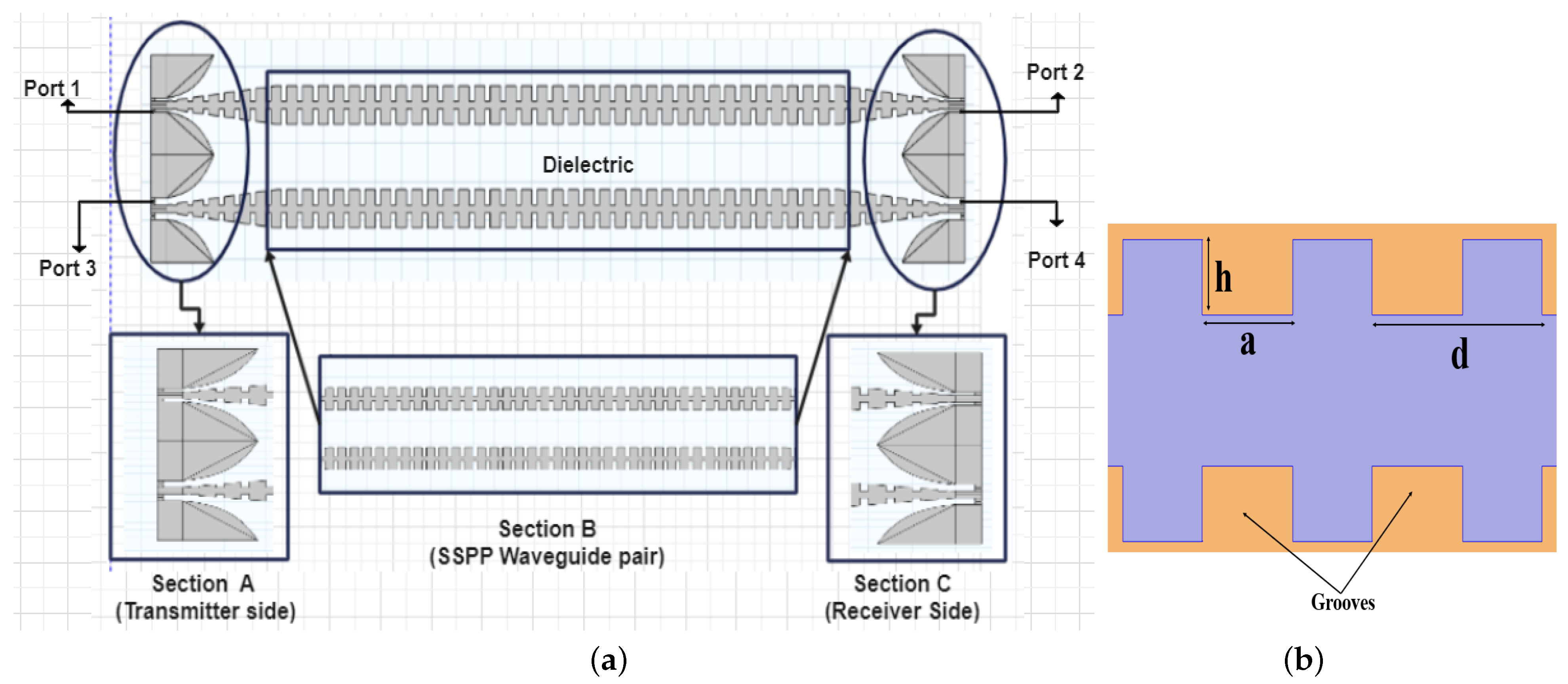
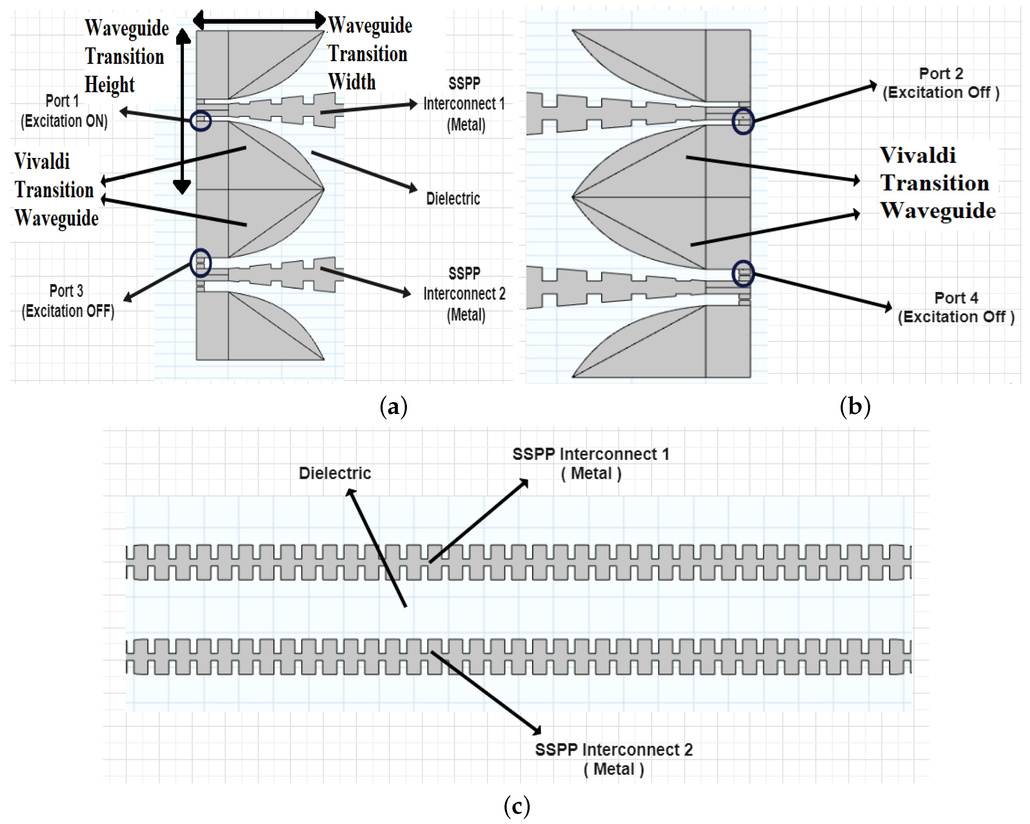
In
Figure 1a, the two dimensional model of two neighbouring SSPP interconnects is shown. The overall 2D structure can be divided into three major parts: section A, B and C.
Figure 2a–c show the detailed descriptions of these parts. There are four ports among which two are in the transmitter side (port 1 and port 3), and the other two ports are in the receiver side (port 2 and port 4). From
Figure 1a, it can be observed that ports 1 and 2 are the transmitter and receiver ports for interconnect 1, respectively, while ports 3 and 4 are the same for interconnect 2. The labelled dimension of an interconnect is shown in
Figure 1b. The grooves are uniform in all geometric parameters and have a height of
h, width
a, period
d and thickness
t.
One of the aims of this study is to investigate the effect of the field distribution of one interconnect on other. Therefore, the input signal is provided only in interconnect 1 and the other ports (2, 3, 4) are left without any excitation. Thus, how much interference is imposed upon interconnect 2 from interconnect 1 can be easily observed. Hence, interconnect 1 is considered as the aggressor wire, while interconnect 2 is termed as the victim wire throughout the study.
The configuration for the transmitting and receiving end of the actual 2D system is depicted in
Figure 2a,b. The device features an adapter that transforms the transverse electromagnetic mode (TEM) into a surface-bound mode for the electrical signal to be transferred via the SSPP interconnect. Each adapter consists of a Vivaldi waveguide transition and grooves, with increasing height, to match the TEM mode with the SSPP mode. The geometry of the waveguide transition is determined using the expressions derived in [
25], where the height (
H) and width (
W) of the waveguide transition are given by the equations
H >
and
W >
, respectively. Here,
and
represents the minimum and maximum operating wavelength, respectively. In this work, the maximum and minimum frequency for SSPP excitation are considered to be 2.8 and 3.25 THz. This corresponds to
= 107.14
m and
= 92.31
m. Thus, according to the above equations,
H should be greater than 99.73
m and
W should be greater than 49.86
m. Hence, the geometry of the waveguide transition is set as follows:
W = 60
m and
H = 100
m. The opening rate,
, is kept at 0.8. Furthermore, for SSPP to be excited, the width of the rectangular ports (1,2,3 and 4) should be
, where
d represents the period of the grooves. As a result, the width of the ports are given as 5
m and the value of the heights is 2.5
m.
This adapter configuration causes the TM mode to propagate through the SSPP waveguide (
Figure 2c) of interconnect 1. The receiving end also consists of a similar structure that converts the SSPP mode back into the TEM mode. As shown in
Figure 2c, each interconnect has periodic metallic corrugation on both sides. In this study, the mutual coupling, or the cross talk phenomena, between the neighbouring wires has been investigated. Only the portions of both interconnects which face each other would interact. Therefore, the modified geometry of
Figure 3a is more suitable for this study instead of the overall 2D geometry of
Figure 1a. In
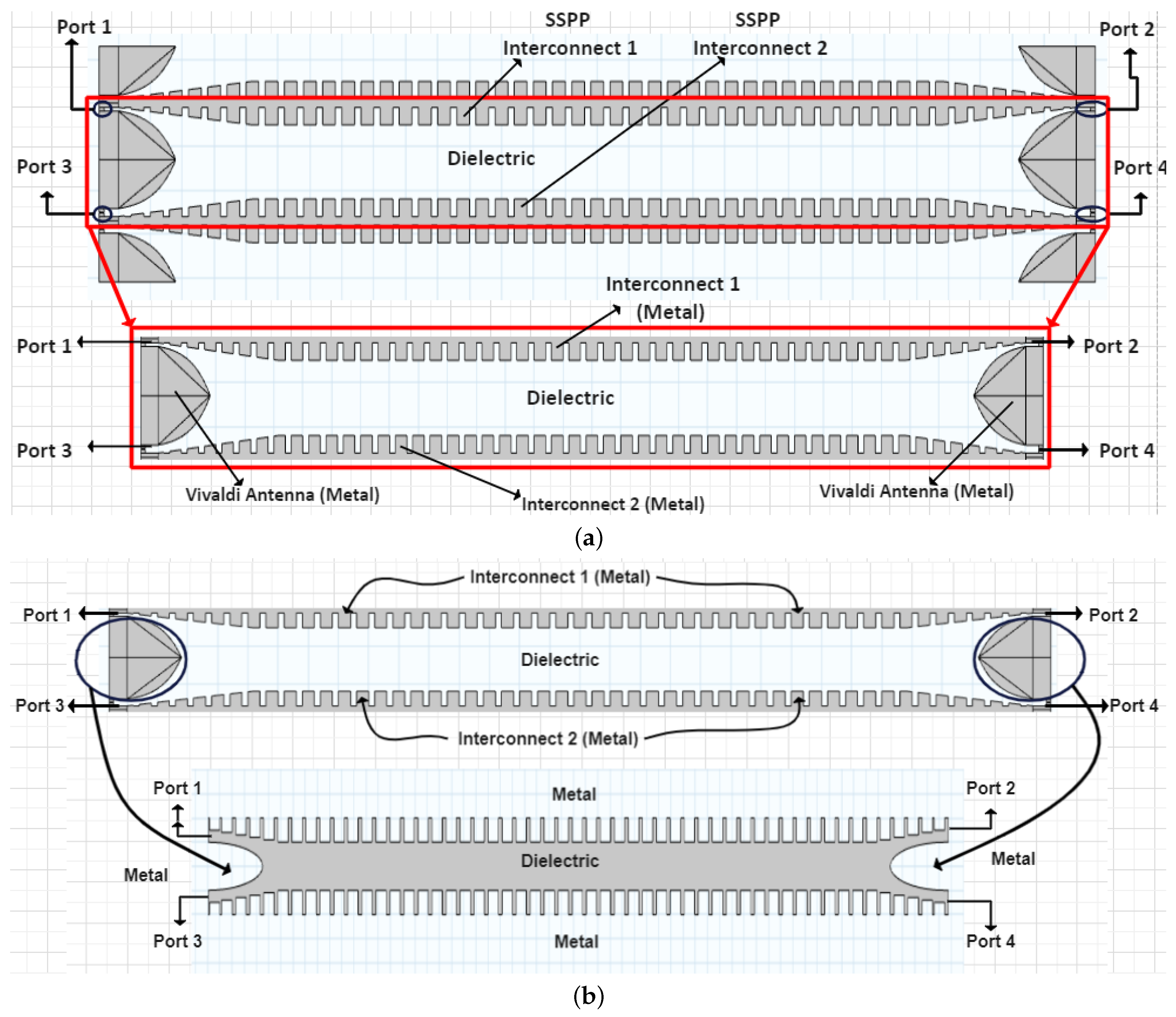
Figure 3a, only the face-to-face parts (enclosed by red box in the figure) from both interconnects are considered for simulation, rather than the overall structure.
Further, some modifications are made on this structure in
Figure 3a, in order to create a convenient architecture of SSPP interconnect pairs for successful simulation in the COMSOL Multiphysics environment. This conversion, or the modification of geometry, is demonstrated in
Figure 3b. From
Figure 3b, the portion between the two metal lines consists of a dielectric. Surface plasmon involves the oscillations of electromagnetic waves in the dielectric medium and also the collective electron oscillations on the metal surface. This results in extremely high field confinement in the dielectric–metal interface. Thus, the electric and magnetic field distributions are found over the dielectric surface between the two metals. Hence the entire region between the two metallic interconnects has been chosen for further analysis. Finally, we have ended up with the form of geometry as shown in
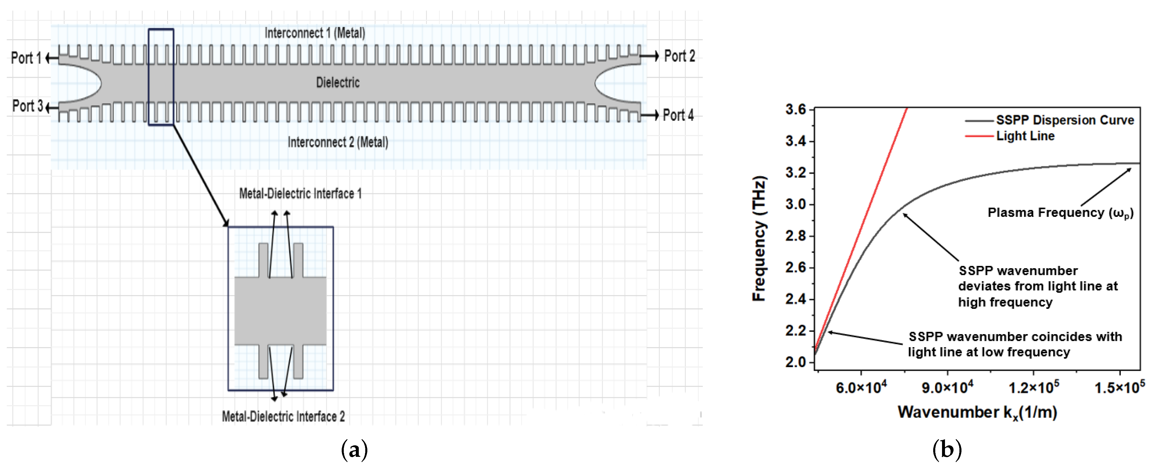
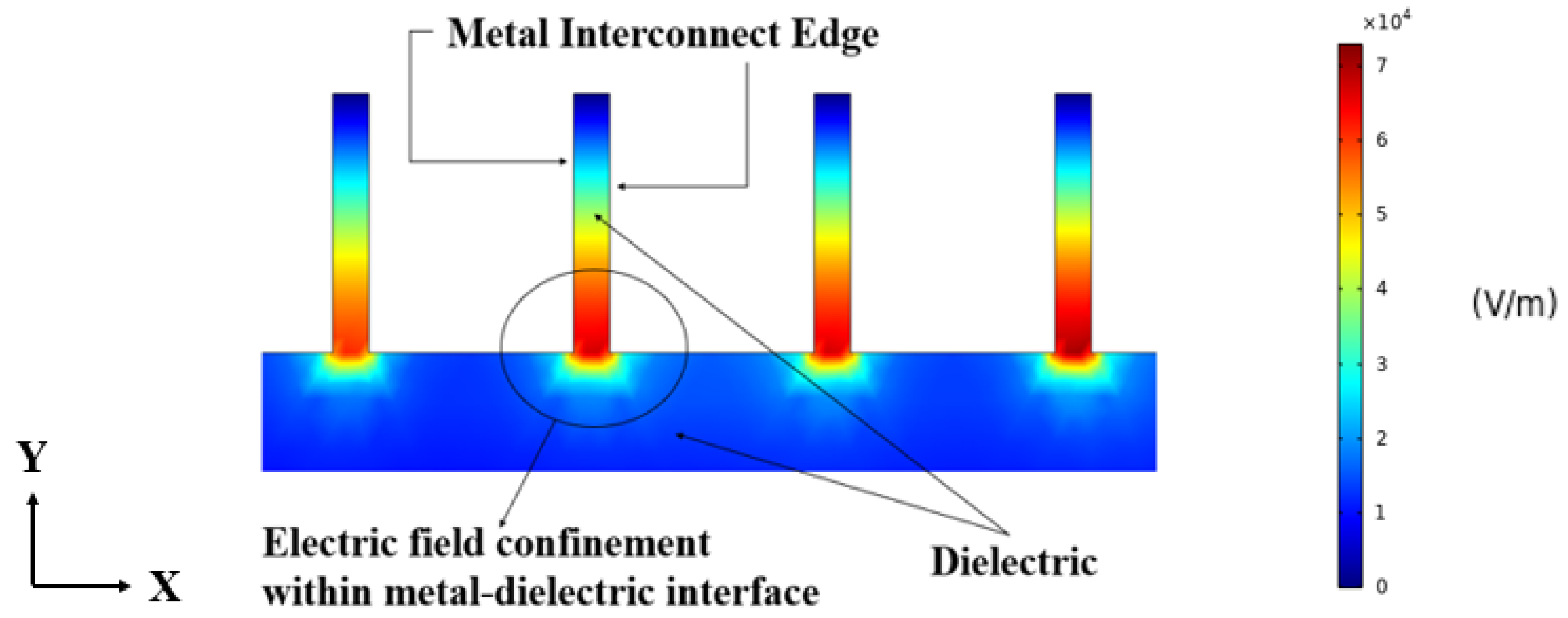
Figure 4a. In this figure, the internal dielectric domain is modelled with two horn-link structures at the transmitter and receiver ends, having four ports in total. Furthermore, a typical portion of identical grooves on both sides of the interim dielectric domain is zoomed and displayed as an inset image in
Figure 4a. The four arrows represent the edges or the corners of metal–dielectric interfaces, where the surface wave field distribution is most likely to be concentrated. In
Figure 5 and
Figure 6a,b, the electric field is observed to be highly confined within these metal–dielectric interfaces, typically indicated by the four arrows in
Figure 4a. The upper two arrows represent the metal–dielectric interface 1 and the lower two arrows represent the metal–dielectric interface 2. Throughout the study, this converted geometry is considered for analyzing the prospects and aspects of SSPP interconnect pairs.
3.2. Geometric Dimensions of Simulated SSPP Waveguide
The geometric dimensions considered in this study are listed in
Table 1. These geometric parameters are determined in such a way that the surface plasmon becomes excited and the interconnect pair should operate within a desired frequency range.
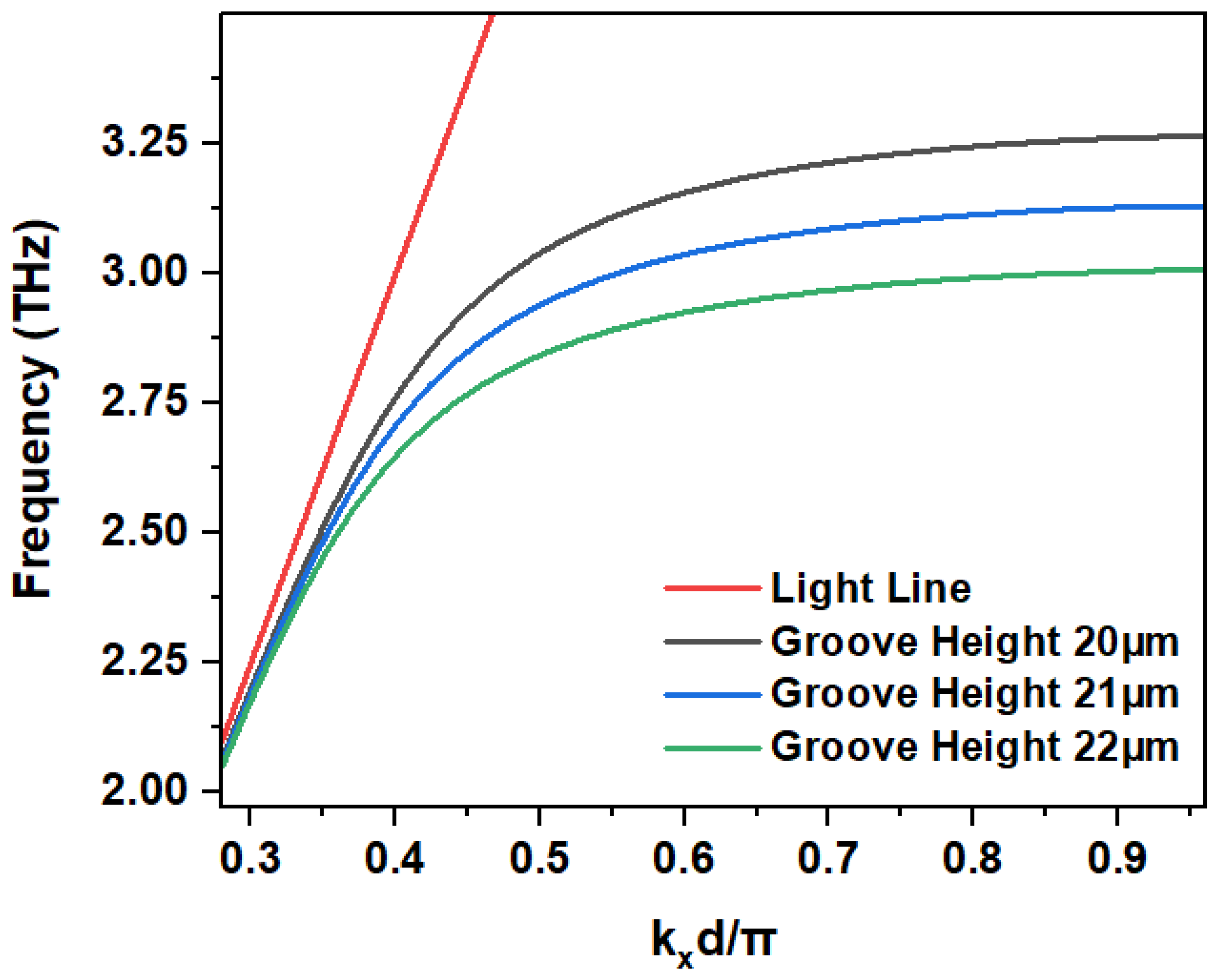
The more we approach the plasma frequency, the more the propagating wave number is deviated from the free space-wave number, which in turn increases the field confinement, self coupling and also reduces the mutual coupling.
Figure 4b shows the dispersion curve of one of the simulated SSPP models with
h= 20
m,
d = 20
m,
a= 3
m and
m = 50. From
Figure 4b, it can be observed that the SSPP dispersion curve coincides with the light line for smaller values of the propagation vector, indicating dispersionless transmission. This also refers to smaller self coupling and higher mutual coupling between two corrugated metal pieces, located on both sides of the interim dielectric, resulting in less electric field confinement. There is an upper cutoff frequency over which the electric field is tightly confined within the metal–dielectric interface. Up to this cutoff, the SSPP channel provides the passbands and above this, it blocks the signal to be transmitted. This cutoff is called the plasma frequency (
) or the resonant frequency of the SSPP waveguide pair.
The SSPP plasma frequency has been chosen to be around 3.25 THz, as shown in
Figure 4b. It has been found that if the operating frequency is far away from the plasma frequency, specially within the lower
portion of the dispersion curve (along the Y axis), then mutual coupling dominates over self coupling [
24] and so the cross-talk increases. Therefore, in order to avoid mutual coupling and to obtain tight field confinement, the operating frequency should be chosen above this cross-talk region of the Y axis, particularly in the upper
part of the dispersion curve (along the Y axis), shown in
Figure 4b.
An analytic expression was derived in [
26] incorporating the relation between plasma frequency and the groove height:
, where
is the desired plasma frequency,
c is the speed of light and
h is the height of the grooves. As the plasma frequency is around 3.25 THz, groove height
h is taken to be 20
m. Later on,
h is varied between 20
m and 22
m to observe the effect of groove height on transmission bandwidth, cross-talk, coupling etc. performance parameters. To support the SSPP mode, the required relation to be maintained between the groove height and groove period is, 2
h >
d [
24,
27]. So, the minimum value of
ratio should be 0.5 to excite the surface wave. To fulfil this postulation, the groove period (
d) is considered as 20
m, so that the
ratio becomes 1 in the proposed design.
For a given period ‘d’ in metasurface, if the ratio decreases, then the field confinement increases for a broader range of frequencies on the fundamental band. It also reduces the cross-talk and ohmic loss in the metal. So, the groove width a is chosen in such a way that coupling factor is small. In this design, the groove width (a) is taken as 3 m so that = 0.15.
The spacing between two interconnects should be 2
h according to [
26]. Hence, the spacing (
x) is considered as 40
m. At first, the number of grooves considered are 50. So, the interconnect length becomes = number of grooves × groove period = 1000
m or 0.1 cm. The last centimetre barrier for a chip-to-chip interconnect is 0.1 cm to 10 cm [
28]. Thus the proposed 2-dimensional SSPP interconnect pair system also satisfies this criterion.
3.3. Simulation by Varying the Dimension
Column 2 of
Table 1 represents the initial or the fundamental values of different geometric parameters. Further, these values are varied in a certain range in order to investigate the dependence of the performance of SSPP channel pairs on these geometric parameters. The fundamental dimensions of the grooves were explained in the previous section. In this section, we discuss about how these fundamental parameters (
a,
h,
d,
m) were varied to observe their effects on the high-frequency data transmission through the SSPP waveguide. While a particular parameter is varied, others are kept constant at their fundamental values, determined by the process described in
Section 3.2.
Table 1 (Column 3) also shows the variation in different parameters used in the study. For instance, the groove height (
h) is varied from 20
m to 22
m to examine how the transmission, cross-talk, bandwidth etc. performance factors change as a result of the change in ‘
h’. Whenever the groove height is varied, the other groove parameters such as width (
a), period (
d) and number (
m) are kept constant at their fundamental values (listed in the 4th column of
Table 1). Thus, each geometric dimension is changed to explore its effect on signal transmission through the SSPP interconnect pair. For all the cases, the distance between interconnects (
x) and the length of the interconnects (
L) are kept constant at their respective fundamental values of 40
m and 1000
m.
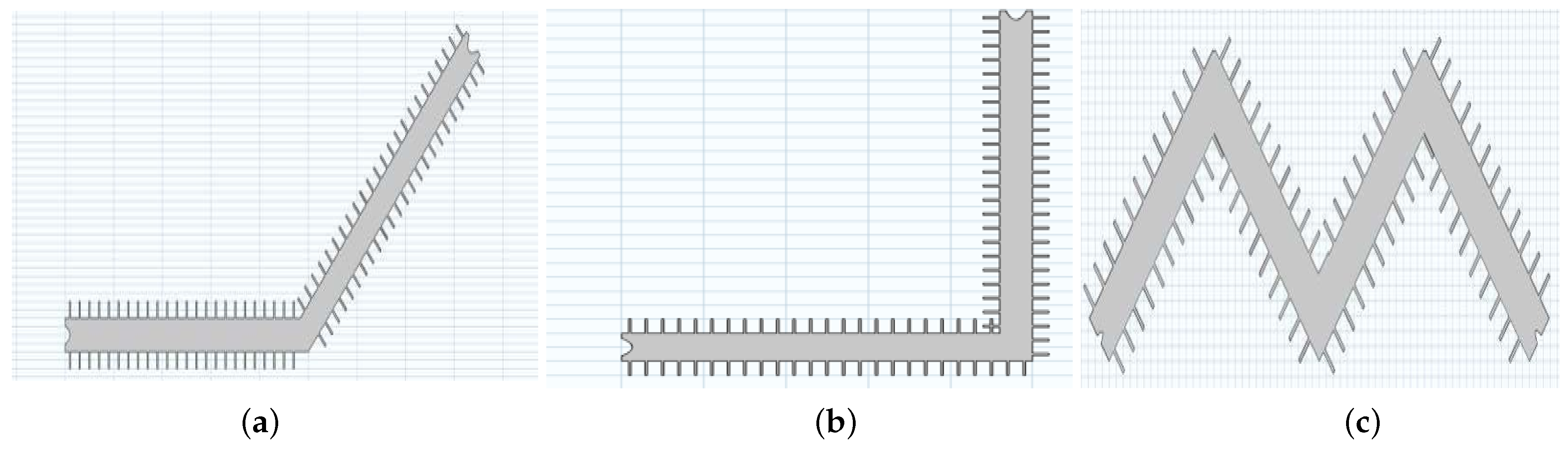
3.4. Simulated Schemes
The trajectory of SSPP interconnects can be of various types on a chip. So, along with the geometric variations in a straight one, four different types of potential wave paths have been considered. Each of these are shown in
Figure 7. The straight interconnect pair is displayed in
Figure 4a. The 45
and 90
bent, and the zigzag SSPP interconnect pairs have also been considered in this study. These are illustrated in
Figure 7a,
Figure 7b and
Figure 7c, respectively. The performances of these structures have been compared with the straight one.
3.5. Simulation Method
For simulation, the frequency domain analysis was used under the RF module of COMSOL Multiphysics 5.5. For this study, several boundary conditions are defined in order to incorporate the surface plasmon polariton physics into the geometry. For a pair of interconnects, two metal–dielectric interfaces exist in the design, as shown in
Figure 4a. One is in between the aggressor wire and interim dielectric, and another one is in between the victim wire and the dielectric.
The main goal of this work is to explore the prospects of SSPP interconnect pairs for ultrafast data transmission. Hence, the converters (TE to TEM, TEM to SSPP and finally SSPP to TE) have been excluded in the model; rather, direct port excitation is given in the from of a Transverse Magnetic (TM) mode, which is supported by the SSPP waveguide.
For direct excitation of the SSPP mode, the ‘port’ feature of COMSOL has been used. Four ports are declared among which two ports (port 1 and port 2) are associated with the aggressor interconnect and another two ports (port 3 and port 4) belong to the victim wire (
Figure 2).
The SSPP mode propagates along the metal–dielectric planar surface and the amplitude of this evanescent component is maximum at the groove and it decays exponentially into the dielectric with increasing distance. Therefore, the surface plasmon mode is modelled with two decaying exponent functions and along the y direction for interface 1 and interface 2, respectively. Here, and are the propagation constants of the SSPP mode at two opposite interfaces. For interface 1, amplitude decreases as we move downwards in the y direction (into the dielectric medium) and for interface 2, amplitude decreases as we go upwards along the y axis. Hence, the TM mode has exponents and for the respective ports.
With these excited surface wave components, the actual TM wave passing through the surface looks like
Here, is the propagating wave along the x direction. A and B are two constants, representing the amplitude of the magnetic field components.
Using Maxwell’s equation,
and are the corresponding electric field components at opposite metal–dielectric interfaces. The conductor edges are defined by the Perfect Electric Conductor (PEC) boundary condition, so that the simulator considers it as the boundary of the metallic interconnect. A scattering boundary condition is used to model the outer environment.
4. Results and Discussion
In this section, we will present the simulation results of the designed SSPP interconnect in detail and conduct a comprehensive performance analysis. Simulations of several SSPP schemes will be performed. In addition, the effect of variations in geometric parameters on SSPP waveguide performance will be investigated thoroughly.
4.1. Electric Field Distribution of SSPP Interconnect Pair
The electric field distributions observed in the finite element study are shown in
Figure 5 and
Figure 6a,b. When excitation is provided in port 1 of the aggressor wire, a surface wave travels the entire region of the dielectric in an oscillatory fashion by coupling both interconnects periodically. During this travel of the surface wave, the electric field distribution is found to be confined within the metal dielectric interface as shown in
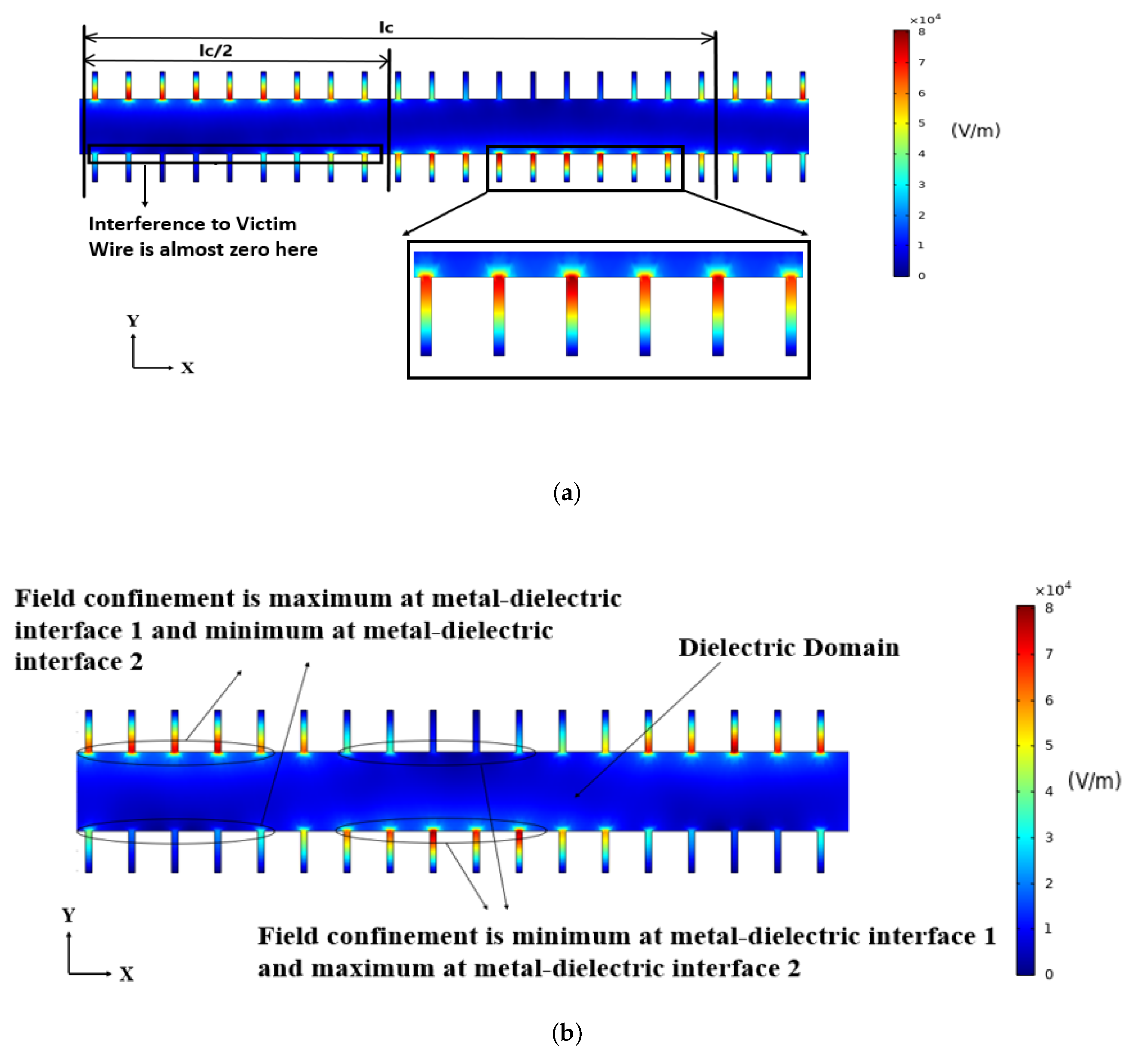
Figure 5. The electric field is trapped inside the cavity, created in between the neighbouring metal interconnect edges. For this high confinement of the electric field within the metal–dielectric interface, the surface wave signal transmission system renders lower cross-talk or interchannel interference. However, there is still a possibility of intra-pair cross-talk. The signal passes through the SSPP interconnect pair with a pulsating nature by engaging both of the interconnects, as shown in
Figure 6b. The electric field distribution is found in the metal–dielectric interface 2, even though the second interconnect of the pair does not have any input excitation. This phenomenon can be regarded as intra-pair cross-talk, since it occurs in between the two connectors of the same pair. This intra-pair interference can also be minimized or mitigated according to
Figure 6b. In
Figure 6b,
lc is called the coupling length. The distance covered by the surface wave, while completing one oscillation, is termed as the ‘coupling length’. For the SSPP pair, shown in
Figure 6a, we can observe that the interference from connector 1 to connector 2 can be reduced to a greater extent, if the length of the pair is half of the coupling length, symbolically
L = lc/2. In that case, the surface wave may reach the receiver of interconnect 1 from the transmitter, without being coupled with connector 2. As a result, the cross-talk in between two connectors of same SSPP pair can be reduced significantly.
4.2. Effects of Variation in Geometric Parameters on Transmission Bandwidth
An important aspect of SSPP technology is that the transmission zones or the bands show prominent dependence on groove height, width, period, groove density, spacing between the corrugated metal pair, etc., geometric configurations of the waveguide pair. These structural parameters can be tuned to transmit a signal within a suitable band through the SSPP waveguide. The dependence of transmission bandwidth on these geometric parameters is discussed in the following subsections, with the necessary simulated plots in COMSOL. The findings of this study have been verified by relevant analytical expressions, empirically derived in previous works.
For all simulations, the port excitation is given in port 1 of the first metal interconnect, and the second one is not provided with any input signal. Therefore, S is considered as the transmission coefficient, i.e., the fraction of the signal being propagated to the other terminal of interconnect 1 and S is considered as the coupling coefficient or fraction of the input signal, being coupled with interconnect 2.
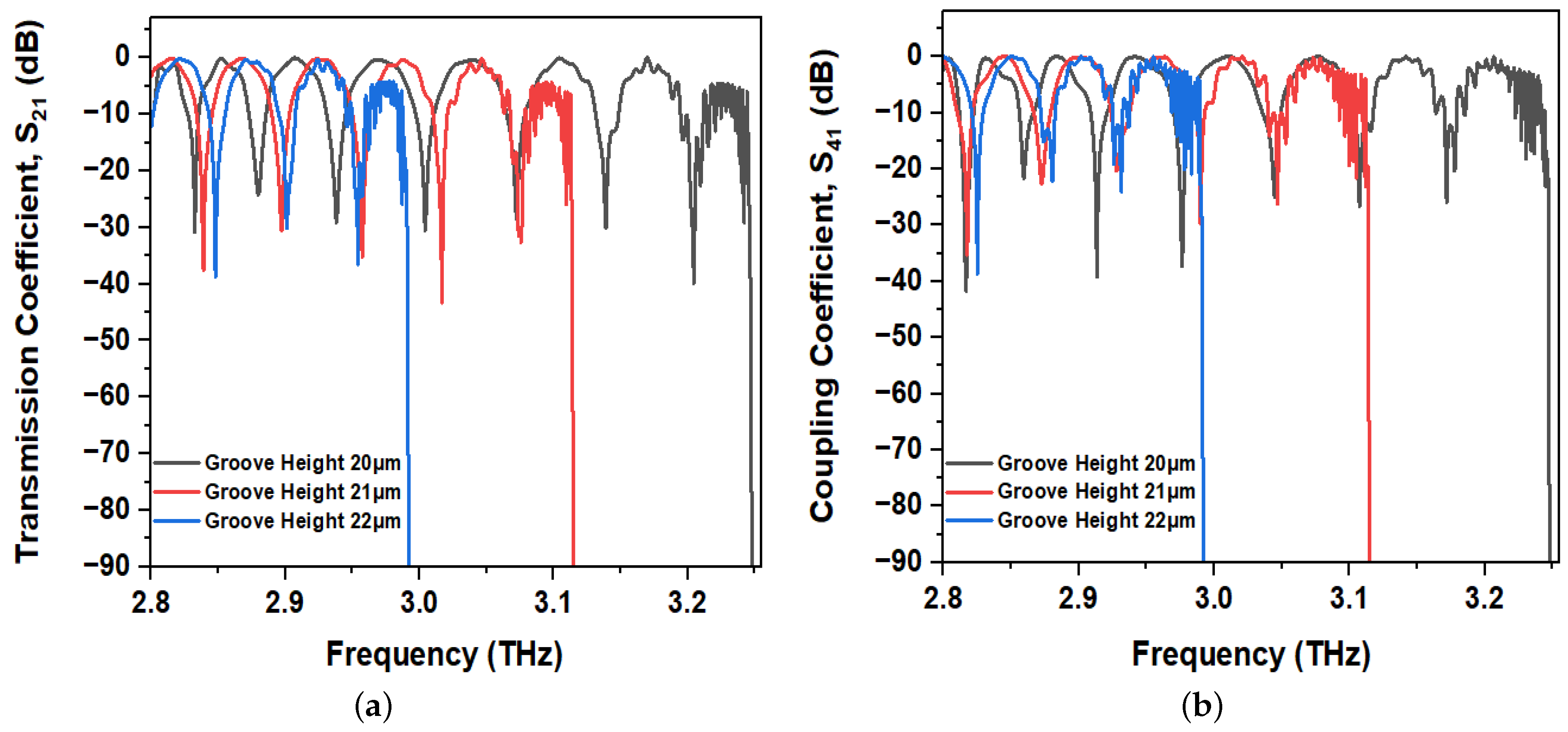
4.2.1. Variation in Groove Height
To examine the dependence of the SSPP bandwidth on groove height, three different heights have been considered: h = 20 m, 21 m and 22 m. In all three cases, the width of the grooves (a = 3 m), the period of the grooves (d = 20 m), the number of the grooves (m = 50) and all other design parameters were kept constant.
Referring to
Figure 8a,b, it can be observed that the transmission and the coupling coefficient show an oscillatory nature and fluctuate periodically. Furthermore, when the transmission reaches its maximum value, the coupling reaches its minimum value and vice versa. For example, at 2.91 THz, the transmission becomes maximum (
Figure 8a) and the coupling coefficient becomes minimum (
Figure 8b). This is true for all the points within the simulated frequency range. This pulsating nature of
and
validates the field confinement within the metal–dielectric interface.
From
Figure 8a, it is also observed that the upper cutoff frequencies of the SSPP channel are around 3.25 THz, 3.12 THz and 2.98 THz for groove height 20
m, 21
m and 22
m, respectively. So, it is possible to draw a relationship between the groove height and the transmission bandwidth. The upper bandwidth frequency decreases as the height of the grooves increases and vice versa. This phenomena can be explained by the analytical expression derived in [
24] as follows:
According to Equation (
6), the SSPP bandwidth is inversely proportional to the height of the groove (
h). So, this theoretical prediction matches with the simulated result for a pair of SSPP interconnects.
The bandwidth change with the variation of groove height can also be explained from the perspective of the wave vector and plasma frequency. The relationship between the SSPP wave vector and the free space-wave vector was derived in [
29] as follows,
where, k
,
a and
h refer to the free space-wave vector, groove width and height, respectively. As the groove height increases, the SSPP wave vector k
differs more and more from the free space-wave vector k
and deviates from the light line (
Figure 9). So, the saturated frequency or the bandedge frequency is achieved quite early, which results in a lower-valued plasma frequency. As the operating frequency goes closer to the plasma frequency, the electric field confinement becomes more and more tight. After the plasma frequency, the electric field is strongly or tightly confined within the metal–dielectric interface. Hence, the carrier surface wave cannot propagate and the signal cannot be transmitted further. This particular frequency is termed as the upper cutoff frequency, above which the SSPP channel pair does not allow any signal to propagate.
In
Figure 9, the plasma frequencies for groove height 20
m, 21
m and 22
m are found to be 3.25 THz, 3.12 THz and 2.98 THz, respectively. That means the plasma frequency decreases as the groove height increases. Therefore, the SSPP channel pair reaches the saturated bandedge frequency i.e., the upper cutoff frequency, earlier and so the bandwidth decreases.
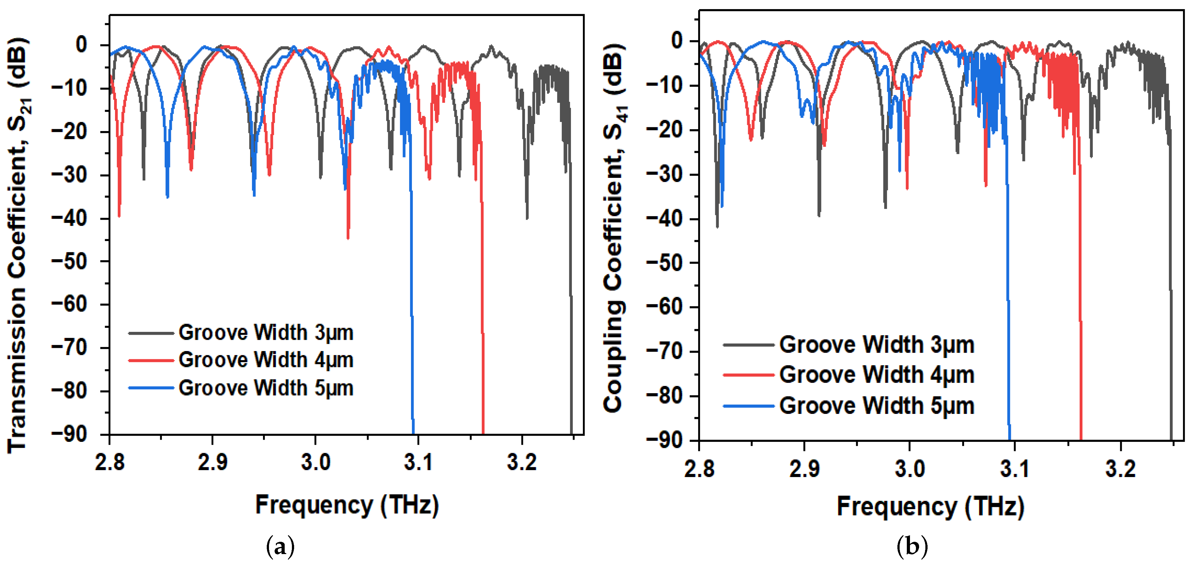
4.2.2. Variation in Groove Width
To examine the dependence of the SSPP data transmission bandwidth on the width of the grooves, three different widths have been considered:
a = 3
m, 4
m and 5
m. In all three cases, the height of the grooves (
h = 20
m), the period of the grooves (
d = 20
m), the number of the grooves (
m = 50) and all other design parameters were kept constant. Here the periodic nature of transmission and coupling coefficient holds as before, e.g., for the groove width of 5
m, at 2.9 THz frequency, the S
reaches at its maximum value (
Figure 10a), while S
goes to its minimum value (
Figure 10b). This is true for all other frequencies within the simulated frequency range.
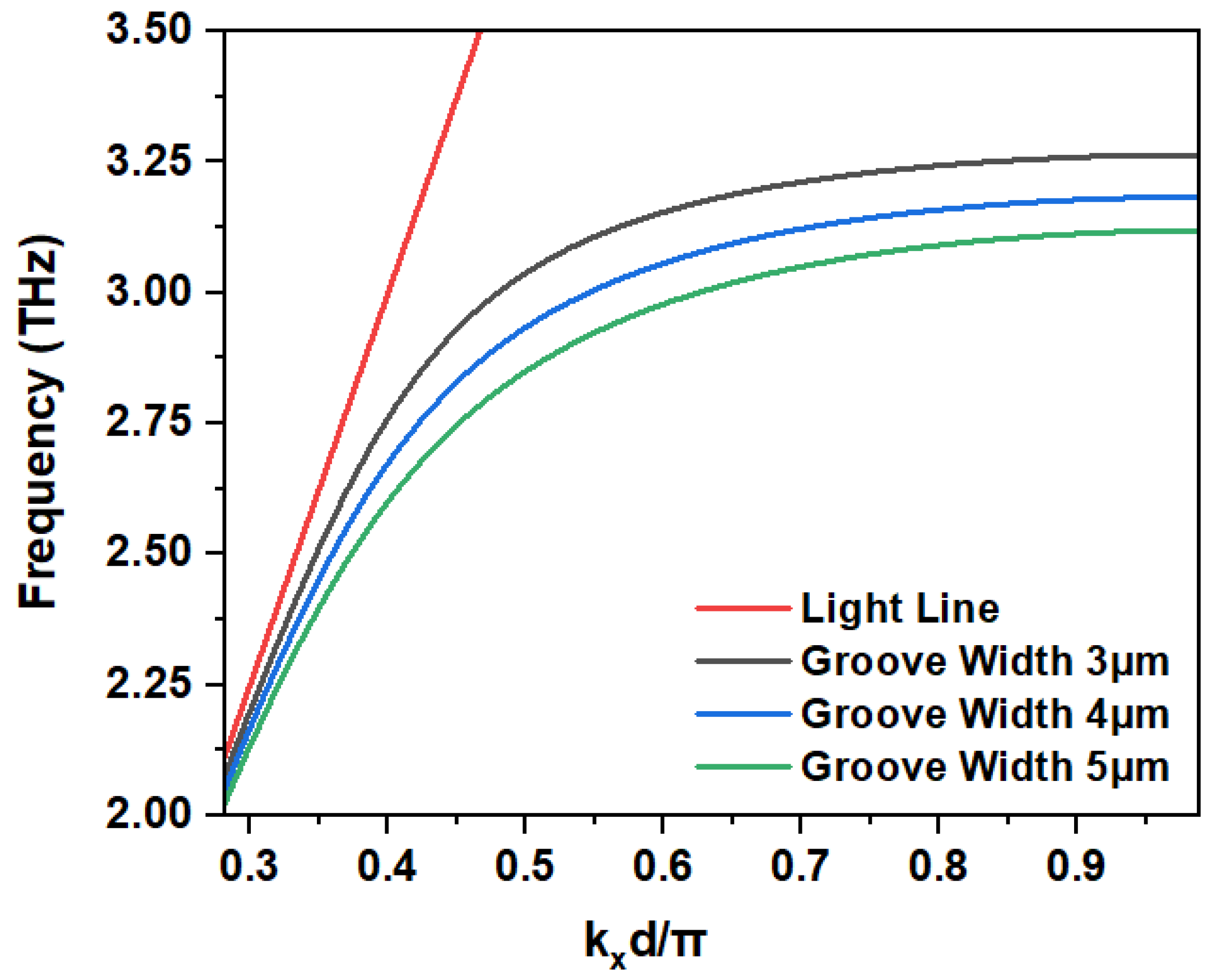
In
Figure 10a, the upper cutoff frequencies are around 3.25 THz, 3.165 THz and 3.09 THz for a groove with widths of 3
m, 4
m and 5
m, respectively. The upper bandwidth frequency decreases as the width of the groove increases. This can be explained by Equation (
6), which shows that increase in groove width causes a decrease in bandwidth.
In
Figure 11, the plasma frequencies decrease as the groove width is increased. That is because, according to Equation (7), the increase in groove width causes a larger deviation of the SSPP wave vector from the free space-wave vector. So, with a 5
m groove width, the SSPP channel pair obtains the maximum field confinement at comparatively lower frequency, which results in smaller bandedge frequency and therefore the upper bandwidth frequency is reduced.
A similar type of dependence of bandwidth on groove height has been observed earlier. However, the effect of width change is comparatively less than that of height change. As per Equation (
6), the SSPP bandwidth has an inversely proportional relation with height but a linear subtractive relation with groove width. Therefore, the groove height is a more prominent or critical factor than groove width to determine the transmission bandwidth of an SSPP channel pair. By comparing
Figure 9 and
Figure 11, it can be observed that the dispersion curves are comparatively closer to each other for width change than the change in height. That means the upper bandwidth frequency is less sensitive to groove width than groove height.
4.2.3. Variation in Groove Density
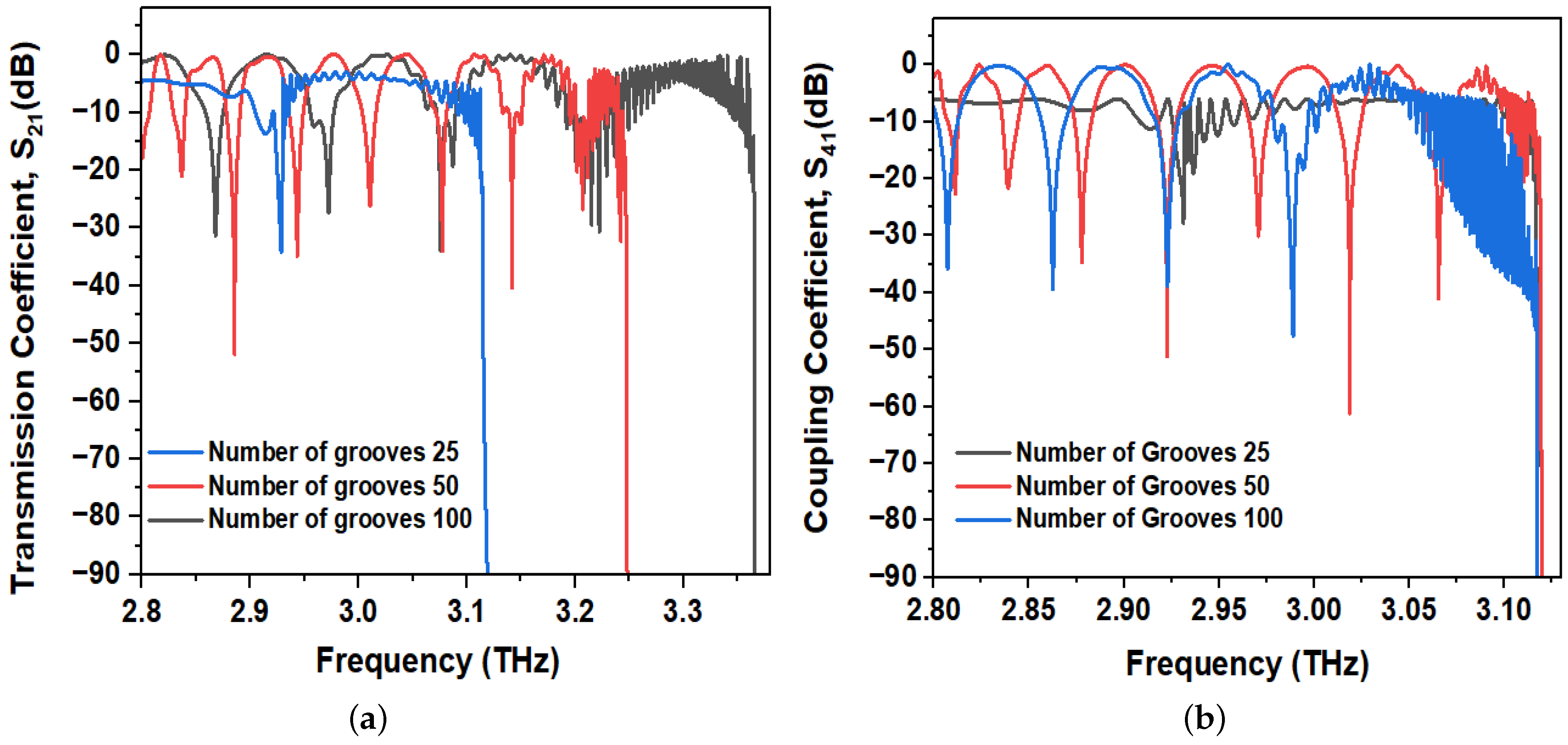
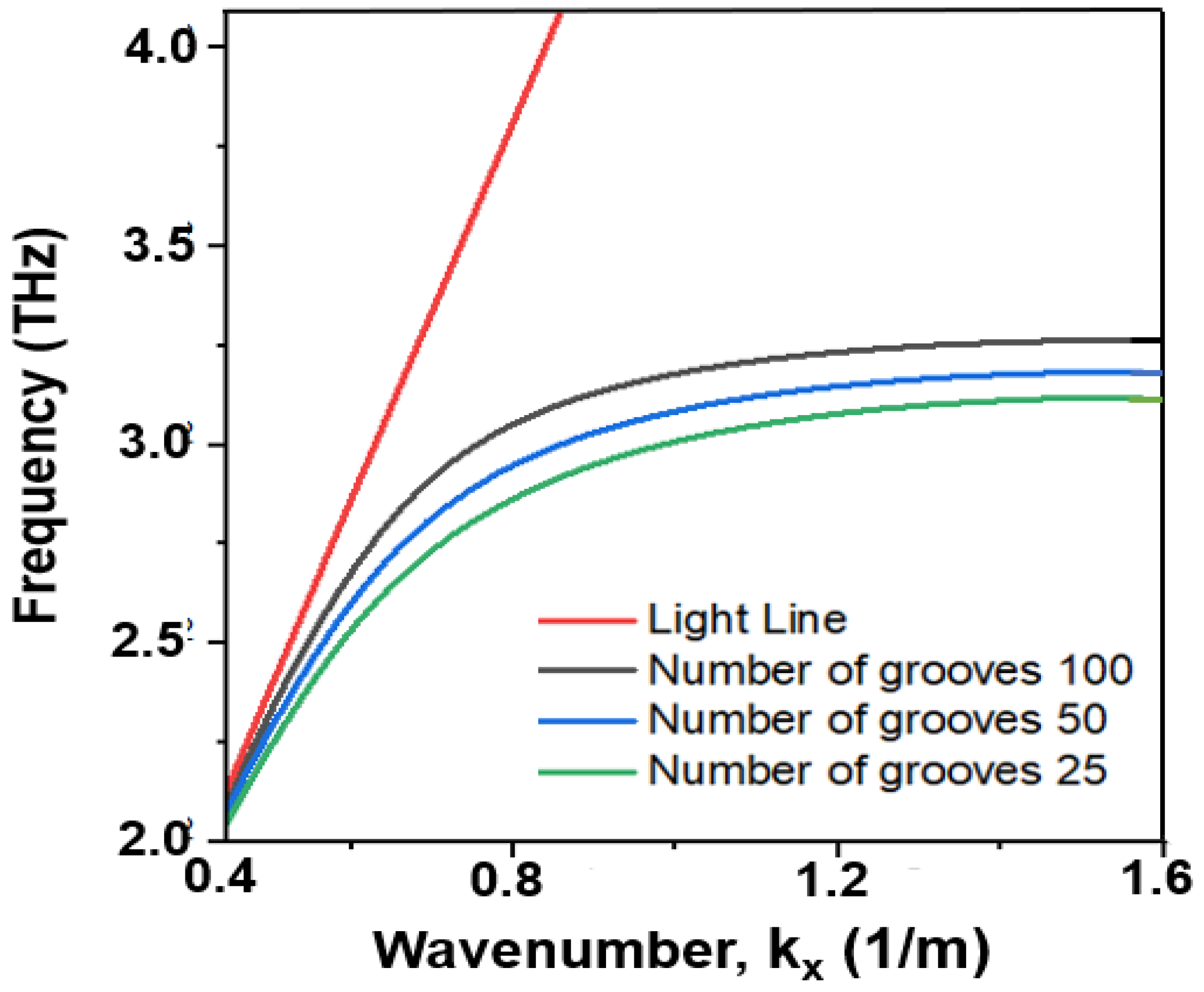
To investigate the effect of groove density on the SSPP channel bandwidth, the number of grooves were varied by keeping the length of the waveguide pair constant. Hence, the period of the grooves (d) was changed to keep the interconnect length (L) the same. In this study, three different groove numbers are taken into consideration: m = 25, 50 and 100. Therefore, the period of the grooves (d) varies by 40 m, 20 m and 10 m for three different designs on a 1000 m length. The other parameters, such as groove height (h = 20 m), groove width (a = 3 m), waveguide length and spacing, etc., are kept constant for all three cases.
The upper bandwidth frequencies (in
Figure 12a) and the plasma frequencies (in
Figure 13) are found to be 3.125 THz, 3.25 THz and 3.365 THz for groove number 25, 50 and 100, respectively. The upper bandwidth frequency of the SSPP channel increases with the increase in groove density, i.e., the decrease in the groove period (
d). As the groove density increases, the grooves becomes closer. Hence, the electric field is more efficiently confined within the metal–dielectric interface, which results in better transmission and eventually larger passbands.
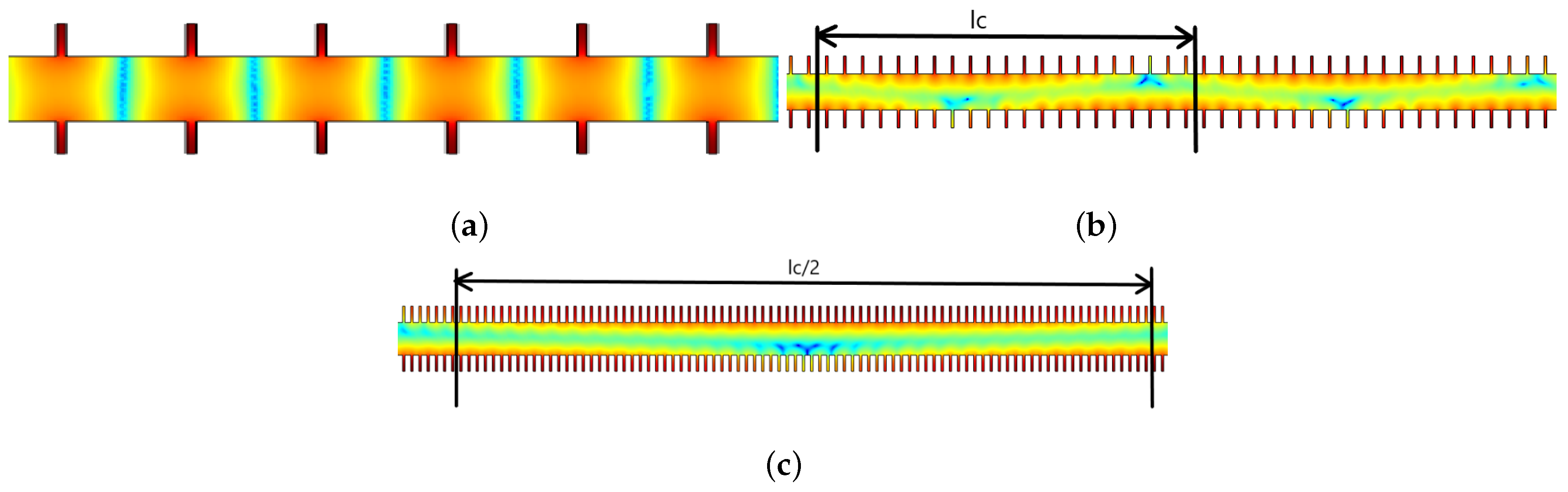
This phenomena of an increase in the SSPP bandwidth with the increase in groove density can also be explained from the perspective of coupling length. In
Figure 14a–c,
lc is called the coupling length. The distance covered by the surface wave, while completing one oscillation, is termed as the ‘coupling length’. The coupling length of the SSPP channel is represented as follows [
24],
As the groove density increases, the periodic gap between the grooves (
d) decreases. The decrease in
d will result in an exponential increase in the coupling length according to Equation (
8), which is visually demonstrated by
Figure 14a–c. As the coupling length increases, the magnetic field distribution is less spread over the interim dielectric; rather, it is more confined within the metal–dielectric interface. It causes more self coupling and less mutual coupling of the magnetic field between two adjacent corrugated metal wires. Thus, the increase in groove density causes an increase in self coupling and a decrease in mutual coupling, resulting in better transmission and larger passbands. The simulated results are verified by the analytical expression of coupling length (Equation (
8)) derived in [
24].
Figure 14a–c show the magnetic field distributions for groove numbers 25, 50 and 100, respectively. These magnetic field distributions of simulated designs support the theoretical prediction as well. For grooves number 25, the magnetic field of both the aggressor (metal 1) and victim wire (metal 2) overlap with each other (
Figure 14a), resulting in higher mutual coupling and lower self coupling. Hence, in
Figure 12a, the transmission coefficient is found to be smaller for groove number 25 than the other two cases. Furthermore, there is no −3 dB band available to transmit data. The magnetic field is mostly distributed over the interim dielectric material. So, the field confinement across the metal–dielectric interface is comparatively lower, and coupling between two interconnects is substantially high (in
Figure 14a).
For a groove number of 50, the magnetic field confinement increases as compared to before (
Figure 14b). In
Figure 14c, for the groove number of 100, the magnetic field distribution is mostly found within the metal–dielectric interface and much less is spread over the interim dielectric. Moreover, the coupling length goes beyond the SSPP pair length considered in this study for
m = 100 (
Figure 14c). Half of the coupling length for the groove number 100 is almost two times that of the total coupling length for a groove number of 50. Therefore, the coupling length is maximum for the groove number of 100 among three cases. That means self coupling is very high and so transmission, along with bandwidth, also increases for the groove number of 100. Thus, field confinement increases with groove density and results in better transmission.
In
Figure 14b, the coupling length increases for a groove number of 50, compared with before (
m = 25). Hence, the mutual coupling or cross talk is expected to be decreased. A further increase in groove number (
m = 100 in
Figure 14c) causes a significant increase in
lc that results in a reduction in mutual coupling or cross-talk. This observation can be verified by
Figure 12b. The coupling coefficient decreases for higher groove density and vice versa. In
Figure 12b, seven minima (below −10 dB) are observed for a groove number of 100; four minima are found for a groove number of 50, while, in the case of a groove number of 25, a single minima is achieved at 2.93 THz. That is, the coupling coefficient seems to increase with a lower groove density, indicating a greater mutual coupling between the two interconnects of the pair. In short, a higher groove density is recommended for greater transmission and less coupling or cross-talk.
4.3. Effects of Geometric Mismatches
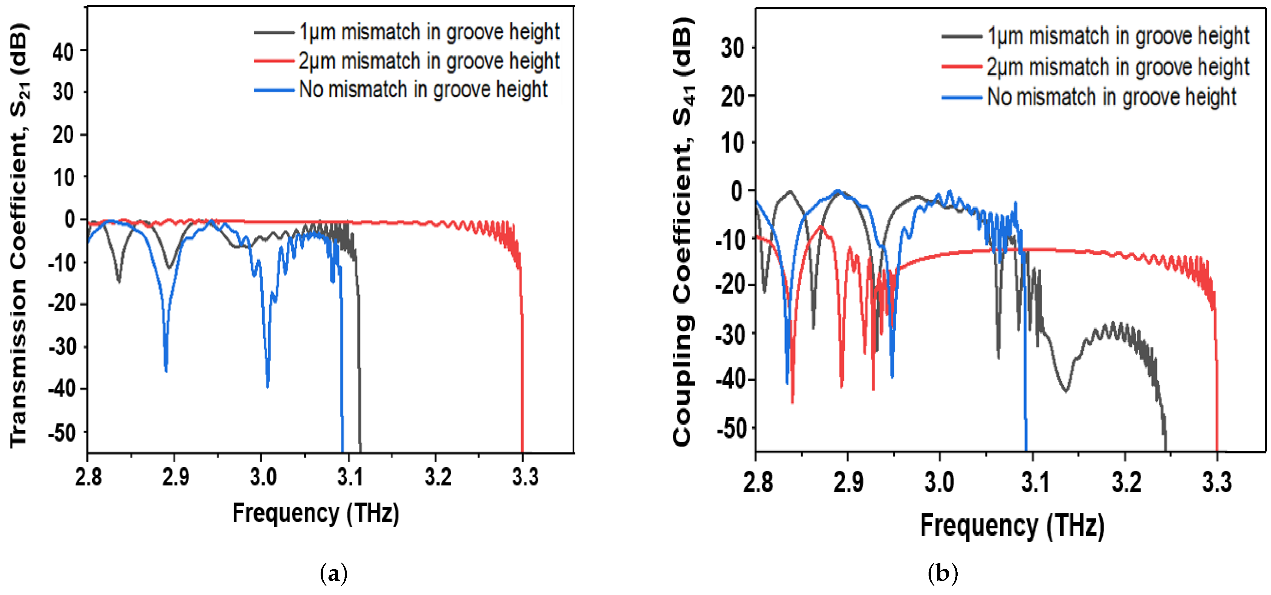
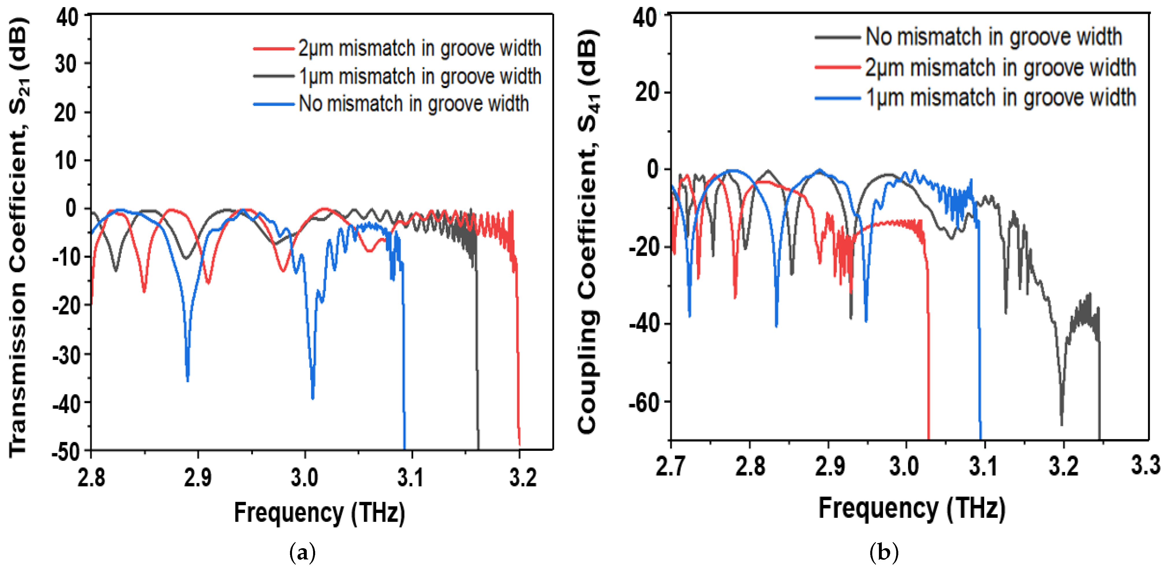
So far, it has been considered that both the interconnects comprising the SSPP channel pair have the same geometric configurations. In this section, the transmission and coupling coefficients have been measured in the presence of mismatches in the geometry. In this study, 1 m and 2 m mismatches are introduced in both groove height and width. One metal wire has h = 20 m, a = 3 m and d = 20 m and another one has h = 21 m, a = 3 m and d = 20 m. Thus, a 1 m mismatch is created in the groove height. Similarly, for a 2 m mismatch in height, one interconnect is considered with h = 20 m, a = 3 m and d = 20 m and the other one is considered with h = 22 m, a = 3 m and d = 20 m.
In
Figure 15a, it is found that for a 2
m mismatch in height, the spectral oscillations near the upper bandwidth decrease and a larger flat zone of transmission is achieved than the 1
m mismatch or no mismatch case. The more mismatch is introduced to the height, the more the middle lobs become flat and consequently the transmission increases. For larger mismatches in height, S
almost coincides with the 0 dB line, rendering a low insertion loss and better transmission. For instance, a much larger passband of almost 400 GHz is obtained when a 2
m mismatch is present in the groove height of both interconnects of the pair (in
Figure 15a).
For no mismatch in height, two minima are found near 2.89 THz and 3 THz, which are below −30 dB (
Figure 15a). The transmission improves, when a 1
m mismatch is introduced in the height of the groove. There is only one minima at 2.84 THz, which renders ∼−15 dB transmission coefficient. After 2.9 THz, no minima is found, rather transmission improves significantly. Finally, for 2
m mismatches in groove height, there is no minima within the simulated terahertz frequency range. That means the transmission loss is nearly zero and almost a lossless transmission is possible. Thus by introducing mismatches in the groove height during fabrication, the transmission can be improved to a larger extent.
Furthermore, from
Figure 15b, it can be observed that the coupling coefficient S
is greatly reduced (below −10 dB) for a 2
m mismatch in height, while the coupling coefficient is much higher for the no mismatch case. Thus, due to mismatches in height, the coupling coefficient gradually decreases, which means that the electric field is mostly confined within metal 1 and less coupled with metal 2. Due to the mismatches in groove height, the two corrugated metal wires show less mutual coupling. So, the electromagnetic energy is more decoupled and confined within the aggressor metal wire (metal 1), which results in better transmission and a lower coupling coefficient.
The effect of mismatches in the groove width has also been explored. For a 1 m mismatch in width, two interconnects are considered. Among them, one has h = 20 m, a = 3 m and d = 20 m and the other interconnect has h = 20 m, a = 4 m and d = 20 m. For a 2 m mismatch in width, one interconnect is considered with h = 20 m, a = 3 m and d = 20 m and the other interconnect with h= 20 m, a = 5 m and d = 20 m.
The same conclusion stands for mismatches in width as well. In
Figure 16a, the transmission bandwidth increases as the mismatch in the groove width is increased. The upper bandwidth frequency is measured as 3.2 THz for a 2
m mismatch in the groove width, which is greater than the 1
m mismatch (3.16 THz) and no mismatch cases (2.98 THz). Furthermore, the transmission coefficient curve almost always remains near the 0 dB line without any sharp fall for the geometry with a mismatch. In
Figure 16a, there is only one transmission minima below −10 dB at 2.85 THz for the 2
m mismatch. However, for the no mismatch case, S
has two abrupt decreases at 2.89 THz and 3.01 THz, where transmission goes below −30 dB, resulting in a high insertion loss.
The result achieved in the transmission graph of
Figure 16a are in line with the insight of the coupling coefficient curve of
Figure 16b. S
generally stays above −10 dB up to 3.12 THz for the geometry without any mismatch in width, while it mostly remains below −10 dB for the geometry with a groove width mismatch. That is, the coupling coefficient (S
) is reduced significantly due to the mismatch in the groove width, as compared to the geometry with no mismatch. That means the mutual coupling or cross-talk will be less in the SSPP pair with a mismatch, as compared to the geometry with no mismatch (
Figure 16b).
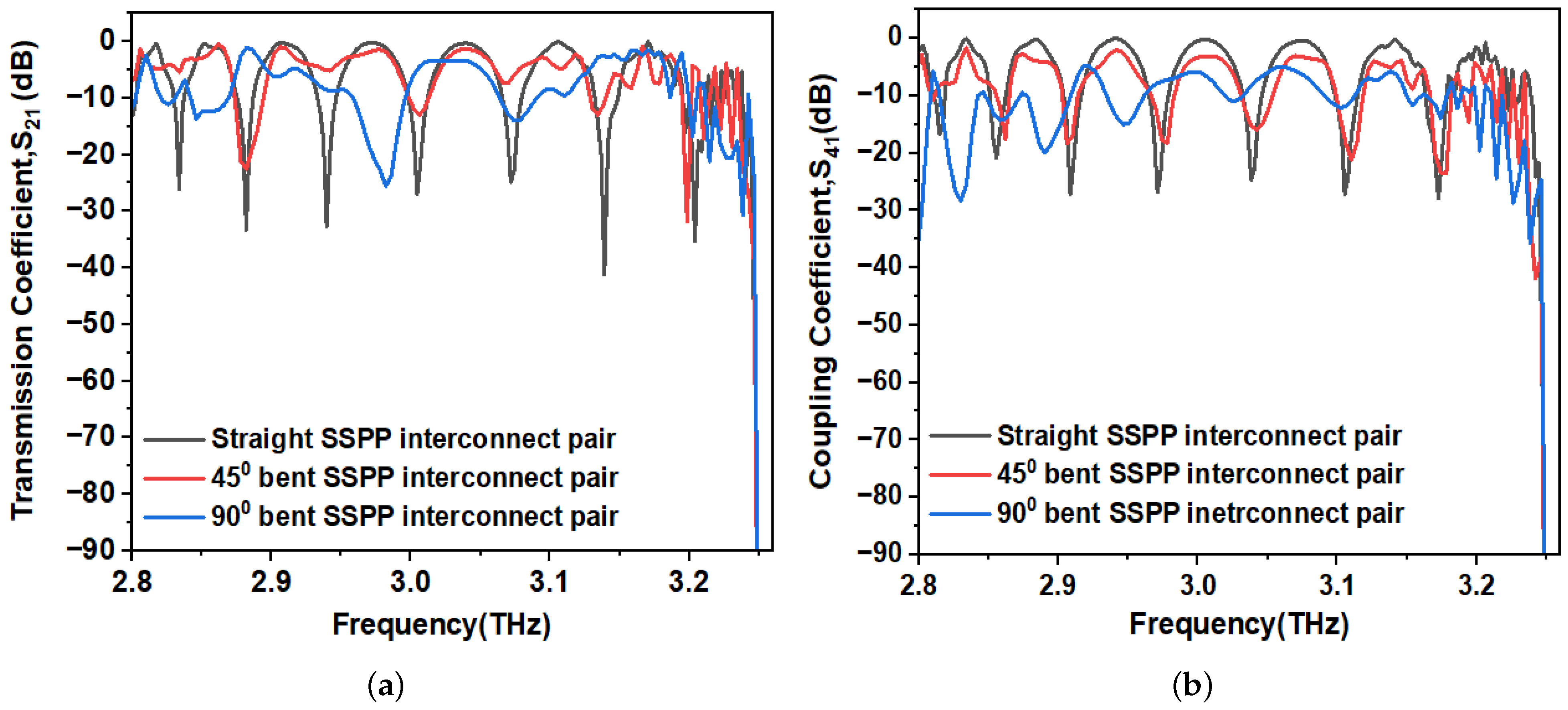
4.4. Effects of Bending
This section investigates the EM energy confinement over a curved path as shown in
Figure 7a,b. In this study, 45
and 90
bent SSPP channels were considered to explore how the transmission and coupling coefficients change due to bending of the waveguide pair.
The upper cutoff frequency of the SSPP channel is found to be approximately 3.25 THz (
Figure 17a) for both straight and bent SSPP channel pairs. That means the upper bandwidth frequency remains almost the same for both types of SSPP waveguide pairs.
In Equation (
6), the upper cutoff frequency of the SSPP channel depends on the geometric parameters of the grooves, such as the groove height, width, density, etc. As all of these parameters are considered to be the same for both straight and bent waveguide pairs, the upper bandwidth frequency remains almost the same for both cases.
However, there is a decrease in the coupling coefficient for bent SSPP channels. For instance, in
Figure 17b, the coupling coefficient mostly remains below −10 dB for the 90
bent interconnect pair, while a larger portion of the S
curve lies above −10 dB for the straight pair SSPP interconnects. As the channel is bent, it creates an inevitable mismatch and so the period of the groove is different in the corrugated interconnects on both sides of the dielectric channel, resulting in two different wavenumbers. Due to the mismatch in groove period, these two metals or interconnects are less coupled to each other when they are bent. For less mutual coupling between the pair of metal wires, the electric field is mostly confined to the aggressor metal (metal 1) itself and so self coupling increases, resulting in an increase in S
and a reduction in S
.
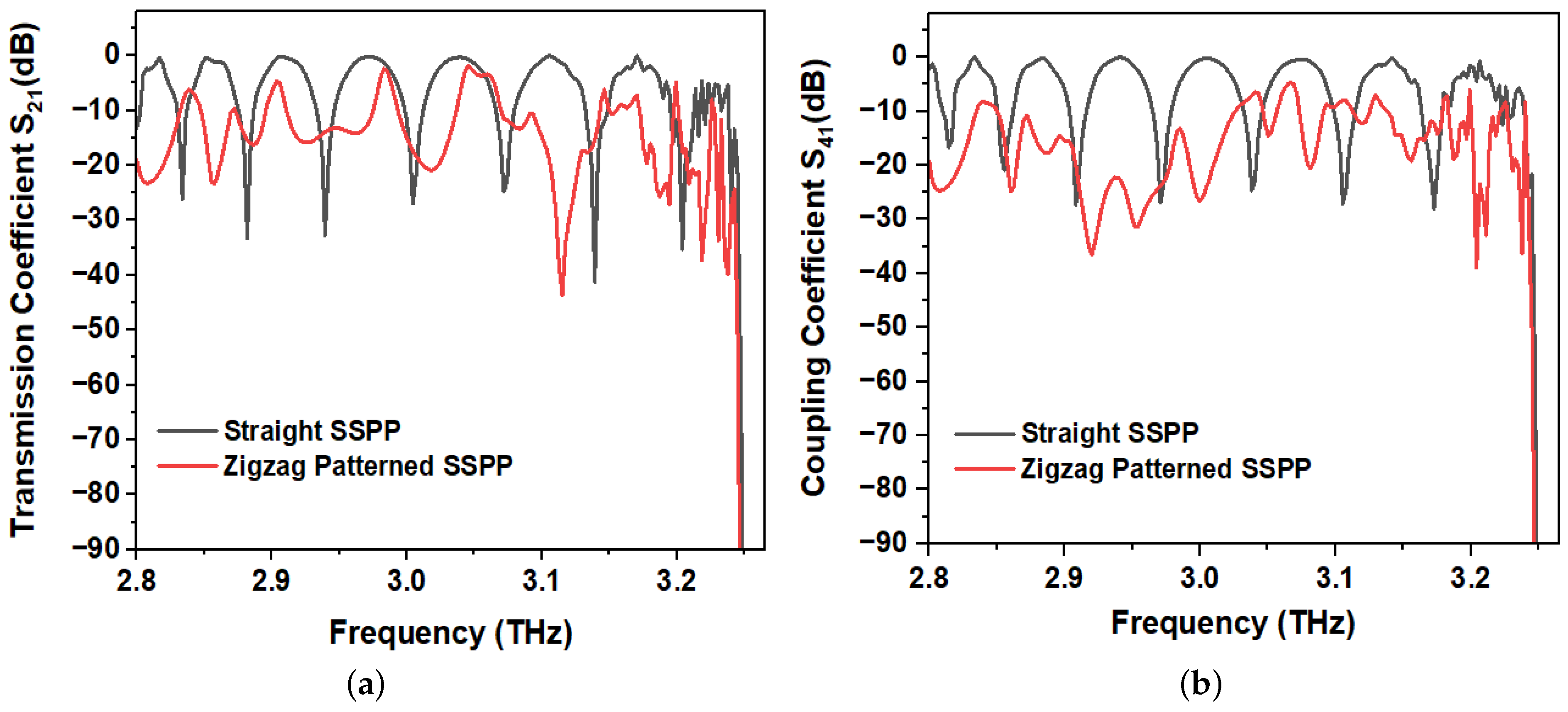
4.5. Effects of Zigzag Pattern
The performance of a more disordered SSPP structure with a zigzag pattern is explored in this section.
Figure 7c shows the geometric design used for the simulation.
From
Figure 18a,b, it can be seen that zigzag patterning causes the transmission and coupling coefficients to change significantly. In
Figure 18b, the coupling coefficient S
falls below −20 dB for most half-power frequency bands. The coupling coefficient also decreases for zigzag SSPP interconnect pairs. The reason behind the reduction in coupling is the structural mismatch introduced in the metal pair, due to the zigzag patterning.
For straight pairs of SSPP interconnects, the interim bands are symmetric and are of equal bandwidths, as shown in
Figure 18a. However, in the zigzag arrangement, the strong coupling between the S
and S
has been lost. The internal passbands or the lobes have lost their symmetric shapes and that is why the −3 dB bands show several different bandwidths. Thus, the oscillatory nature of electromagnetic energy deteriorates while the SSPP waveguide pair is patterned in a zigzag path.
5. Performance Summary and Comparison
In this section, the proposed surface plasmon polariton-based interconnect technology is compared with state-of-the-art SSPP interconnects. Several performance parameters such as transmission coefficient (S
), reflection coefficient (S
), bandwidth, available passbands of SSPP channel pair, etc., have been considered for comparison. These parameters obtained from this study are listed in
Table 2, while these performance parameter values achieved in the state-of-the-art works are shown in
Table 3.
The performance of the SSPP waveguide due to variations in geometric parameters has been investigated thoroughly. Seven designs are selected from various simulations performed in this study and are summarized in
Table 2. In designs 1–3, the groove width (
a) is varied from 3 to 5
m and the groove height (
h), period (
d) and number of grooves (
m) are kept constant. Designs 4 and 5 maintain a constant groove density and width while varying the groove height from 21 to 22
m. In design 6, the groove density is doubled as compared to previous ones. Finally, in design 7, a 2
m mismatch in height is introduced.
Designs 1–3 show that as the groove width increases, the upper cutoff frequency decreases. This relation has already been verified in the previous sections. The simulations in
Section 4 shows that several lobes are present within the simulated frequency. These lobes are referred to as internal passbands. The third column in
Table 2 represents the range of frequencies within the internal passbands for which the transmission coefficient is above −3 dB. To give an example, for the straight SSPP interconnect pair (Design 1) with
h = 20
m,
d = 20
m,
a = 3
m and
m = 50, there are six available passbands in the THz range. The bandwidth gradually increases from 21 GHz to 34 GHz and again starts to decrease as we approach the upper cutoff frequency of the SSPP channel, and finally end up with a band of 20 GHz before the cutoff. Furthermore, the number of passbands decreases as the groove width increases. However, the bandwidth of the internal passband tends to increase. Additionally, column 6 and column 9 of
Table 2 provide the average transmission and reflection coefficients inside the internal passbands. The inverse relationship of the upper cutoff with the groove height is illustrated in designs 4 and 5. The number of passbands decreases as the bandwidth decreases, and this trend continues. Design 6 summarizes the results of bandwidth tuning by changing the groove density. In comparison to design 1, the groove density is doubled, which results in an increase in the upper cutoff and internal passband bandwidth as well. This happens as the waveguide’s internal self coupling increases. Design 7 does not follow the trend explained from designs 1 to 6. This is because mismatch is introduced between the pair of SSPP interconnects for which coupling between them decreases significantly. Therefore, the oscillatory nature is diminished and a single band of around 400 GHz is obtained.
From
Table 3, it can be observed that most of the previous researchers have worked with SSPP interconnects operating in the gigahertz range. For example, 2–14 GHz, 0–10 GHz, 6–11 GHz and 46.1–73.7 GHz are the simulated frequencies found in [
18,
30,
32,
33], respectively. However, the existing electrical connectors show fairly good performance in the gigahertz frequency. So, it is not feasible to install a novel technology, e.g., an SSPP waveguide, for data transmission in the gigahertz range. Rather, the conventional interconnects suffer from phenomena such as cross-talk, energy loss, signal reflection, etc., which severely degrade the data transmission performance in the terahertz frequency range. In this regard, surface wave signal transmission can be a good alternative due to high field confinement, larger bandwidth and less reflection. That is why performance evaluation of the SSPP waveguide within or beyond the terahertz range is more viable and relevant. Therefore, this study aims to explore the terahertz characteristics of surface plasmon channels for ultrafast data communication.
Table 2 shows the summary of the proposed design, simulated in the terahertz range. As shown in
Table 3, some recent research on SSPP waveguides based on terahertz frequencies [
22,
23]. In addition, we compared the proposed SSPP design with the research reported in [
35,
36,
37,
38,
39]. The simulated structures of this study perform significantly better than the existing ones in terms of SSPP channel bandwidth. In the proposed design, multiple −3 dB bands are available to transmit data for each SSPP waveguide as listed in
Table 2. Additionally, design 7 provides the maximum available bandwidth among the other ones within a single band. For designs 1–6, the bandwidths of internal passbands are large enough to use them as an ultra-wideband channel. Furthermore, approximately 50% of the total bands have bandwidth in the range of 20–30 GHz; 36% of bands have a bandwidths in the 30–40 GHz range. Furthermore, few bands are found to have much a larger bandwidth (>40 GHz). In the existing works, −3 dB bandwidths are found to be 20 GHz, 13 GHz, 4 GHz, 27.6 GHz, 60 GHz and 40 GHz in [
11,
18,
32,
33,
38,
39], respectively. The bandwidths are significantly higher in [
35,
36,
37], about 100 GHz. In addition, bandwidths of 300 GHz and 250 GHz are observed in [
22,
23]; however, design 7 of this study, as shown in
Table 2, far exceeds them (∼400 GHz).
The proposed structures are designed to operate in the frequency range of 2.8 to 3.25 THz. Design 7 has a bandwidth of 400 GHz with an upper and lower cutoff frequency of 2.82 THz and 3.22 THz, respectively. Thus, the structure has a transmission coefficient of higher than −3 dB for almost the entire simulated range. In terms of fractional bandwidth (FBW), design 7 has a value of 13.25%. This value is lower than those of [
22,
32,
33,
35,
38], which have values of 32.2%, 25%, 45.8%, 27.03% and 20.7%, respectively. Although a relatively large bandwidth (400 GHz) is available, the value of the FBW indicates narrowband transmission of signals in the terahertz regime.
From the perspective of reflection and transmission coefficients, the proposed designs exhibit improved performance. The transmission coefficient is found to be within 0 dB to −0.5 dB for all of the simulated designs in
Table 2. Especially for Design 6 (
Table 2), the transmission coefficient is measured to be almost 0 dB (−0.05 dB). That means nearly lossless transmission is possible in this geometric configuration of SSPP waveguide. Signal reflection is also significantly reduced in the simulated SSPP structures. For most of the designs in
Table 2, the reflection coefficient is below −11 dB. For some bands,
goes below −20 dB (design 1 and design 2), which is better than the designs compared in
Table 3.
In addition, the designs support odd mode SSPP. This can be verified by
Figure 7, which shows the electric field distribution in between the two SSPP waveguides. The figure shows that the electric field is confined within the grooves at the metal–dielectric interface, i.e., it does not penetrate deep inside the metal region. Thus, if a single SSPP waveguide is considered, an antisymmetric field distribution can be observed. This antisymmetrical distribution is referred as an odd mode SSPP, the significance of which has been discussed in [
40,
41]. Generally, SSPP propagation can be classified into two types: odd and even mode.
In even mode, the electric field penetrates deep inside the metal surface and creates a continuous electric field inside it. As a result, the conductor’s internal field distribution is symmetric, and the integral of the electric field is zero along its cross section. Consequently, the even mode cannot support the internal potential difference. Thus, an external ground is required for signal propagation. On the other hand, in odd mode, the integral of the electric field has a non-zero value along the cross section because of the asymmetrical field distribution. Hence, an internal electric potential difference is generated. Thus, no external ground is required for signal transmission. Therefore, the designs presented in this work are also suitable for single-conductor integration. In chip designing, the exclusion of a ground wire allows for more compact assembly and space savings. Additionally, unlike electrical interconnects where both power and ground wire are present, a significant amount of mutual capacitance is observed, whereas for single conductors, no such phenomenon occurs.
According to the previous findings in
Section 4, the transmission improves with a lower groove height, width, period and higher number of grooves. Among all of our simulated structures, design 6 has the required dimension with smaller groove height, width and higher groove density. Hence, design 6 in
Table 2 shows best performance, with higher transmission (−1.27 dB) and minimum reflection (−13.76 dB). However, with respect to bandwidth, design 7 has the clear edge over the others. So, it can be concluded that the SSPP interconnect pair of design 6 and 7 are the winning designs of this study.


