Article

White Rabbit Expansion Board: Design, Architecture, and Signal Integrity Simulations

IFIC—Instituto de Física Corpuscular (CSIC—Universitat de València), c/Catedrático José Beltrán, 2, 46980 Paterna, Spain
*
Author to whom correspondence should be addressed.
Electronics 2023, 12(16), 3394; https://doi.org/10.3390/electronics12163394
Submission received: 29 June 2023 / Revised: 4 August 2023 / Accepted: 8 August 2023 / Published: 10 August 2023

Abstract

:
The White Rabbit protocol allows synchronization and communication via an optical link in an integrated, modular, and scalable manner. It provides a solution to those applications that have very demanding requirements in terms of synchronization. Field-programmable gate arrays are used to implement the protocol; additionally, special hardware is needed to provide the necessary clock signals used by the dual-mixer time difference for precise phase measurement. In the present work, an expansion board that allows for White Rabbit functionality is presented. The expansion board contains the oscillators required by the White Rabbit protocol, one running at 125 MHz and another at 124.922 MHZ. The architecture of this board includes two oscillator systems for tests and comparison. One is based on VCOs and another on crystal oscillators running at the desired frequencies. In addition, it incorporates a temperature sensor, from where the medium access control address is extracted, an electrically erasable programmable read-only memory, a pulse-per-second output, and a USB UART to access the White Rabbit IP core at the field-programmable gate array. Finally, to ensure the quality of the layout design and guarantee the level of synchronization desired, the results of the power and signal integrity simulations are also presented.

1. Introduction

Many applications have very stringent requirements in terms of synchronization. In telecommunications, the performance of 5G New Radio and next-generation technologies rely on phase synchronization of Radio Access Network (RAN) nodes [1,2,3]. In data centers, time synchronization is needed for data consistency, task scheduling, and resource sharing [4]. Particle physics experiments, where the trajectory of relativistic particles has to be determined with high precision, require a high level of synchronization. For instance, in neutrino telescopes [5,6,7,8,9] the synchronization requirements are at the level of the nanosecond. Similar requirements are also needed in astrophysics detectors such as Auger [10], SKA [11], or CTA [12]. Therefore, it is mandatory for these applications to develop systems that incorporate a high-level synchronization facility. The White Rabbit (WR) protocol allows for subnanosecond synchronization and deterministic data transfer via optical fibers, making it an ideal solution. However, the implementation of the WR protocol requires specific hardware. An IP core, the White Rabbit PTP core (WRPC) [13], which is available for several field-programmable gate array (FPGA) architectures (Virtex6, Artix7, Kintex7, Virtex7, Ultrascale, Ultraescale+, Arria II, and V) [14], provides the synchronization functionality. Additionally, two clocks running at frequencies of 125 MHz and 124.992 MHz are needed by the digital dual-mixer time difference (DDMTD) running at the FPGA for precise phase measurement. This work presents an expansion board that includes all the necessary hardware to operate the WR protocol, facilitating the use of this protocol in an already existing FPGA board. The WR protocol is discussed in Section 2, while the design of the expansion board is presented in Section 3. The pre-layout signal integrity analysis performed on the design and the results of the virtual prototyping analysis are presented in Section 4. Finally, some conclusions and future plans are presented in Section 5.

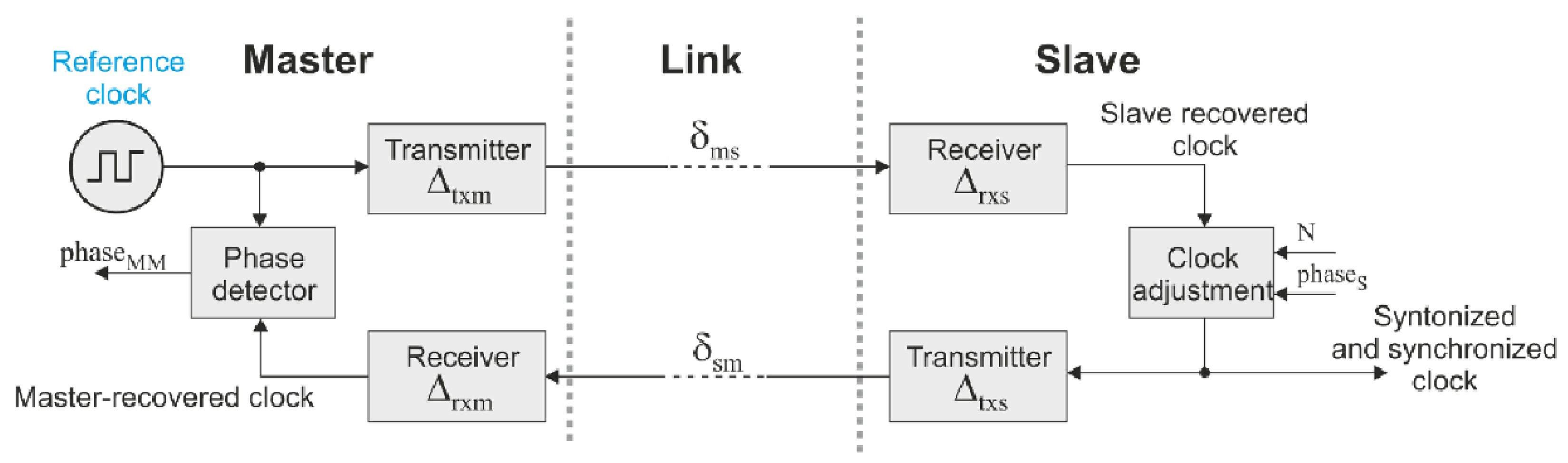
2. White Rabbit Protocol

WR is an open-source project developed by an international collaboration [15] and stored in the Open Hardware Repository at the European Organization for Nuclear Research (CERN), the main promoting institution. Data transmission and synchronization are provided via Ethernet [13,16], ensuring subnanosecond synchronization and deterministic data transfer by using PTP [17,18] and Sync-E [19]. It has been designed to provide precise synchronization of clocks over packet-based networks, and recently it has been adopted by the latest PTP standard [20], IEEE 1588 HA with a guarantee that the accuracy of the resulting synchronization is better than one nanosecond [21]. Its goal is to provide nanosecond-level synchronization accuracy over wide area networks, and can be used to synchronize distributed systems, such as high-energy physics experiments [22,23,24], power distribution grids [25], control or measurement systems, with applications such as short-circuit fault location [26]. The protocol is based on an end-to-end concept, meaning that a source node broadcasts its timestamp, and the receiving node uses this timestamp to synchronize its local clock. WR uses a distributed master-slave architecture, which allows for high accuracy and scalability. In a WR master-slave network, the master hierarchically controls several slaves, distributing the synchronization down the network. The topmost WR master in the hierarchy, synchronized with Global Positioning System [27,28], provides time to lower layers. Synchronization is achieved by accurately measuring the delay from master to slave. The slave clock is synchronized with the master, and the phase shift is accurately measured by the key element of WR, the DDMTD phase detector [29]. The operation of the DMDT requires two very precise clock signals of 125 MHz and 124.992 MHz. These two signals can be generated by voltage-controlled oscillators (VCOs) or by oscillators oscillating at that precise frequency. A special hardware, that needs to be available to any WR device, provides these two clock signals. The phase noise of the two clocks is directly affecting the level of synchronization obtained. Therefore, careful implementation of the DDMTD hardware is required. The basic synchronization operation of WR includes measuring the round trip time, adjusting for the hardware delays in the master and slave ( Δ t x m , Δ r x m , Δ t x s and Δ r x s ), and the asymmetry of the fiber interconnecting the slave and the master ( α ). The WR model is shown in Figure 1. The asymmetry of the fiber is caused by different transmission speeds for the uplink and the downlink, which can be computed using the refractive indices of the respective wavelengths ( n λ 1 and n λ 2 ). Experimentally, α can be determined by measuring the up-link and down-link transmission time ( δ s m and δ m s ) in the lab:
α = n λ 1 n λ 2 1 = δ m s δ s m 1
A PTP package is used to measure the time of emission and reception of data between the master and the slave. The round trip time is computed using the values measured at the master ( t 1 , t 4 ) and the slave ( t 2 , t 3 ). Additional values such as the fixed hardware delays ( Δ = Δ t x m + Δ t x s + Δ r x m + Δ r x s ) and the fiber asymmetry ( α ) are also taken into consideration when calculating the delay from the master to the slave ( d e l a y m s ). This is achieved using the following equation,
d e l a y m s = 1 + α 2 + α × ( d e l a y m m Δ ) + Δ t x m + Δ r x s
Thanks to this, the clock in the slave can be adjusted and both devices can be synchronized with a precision lower than one nanosecond.

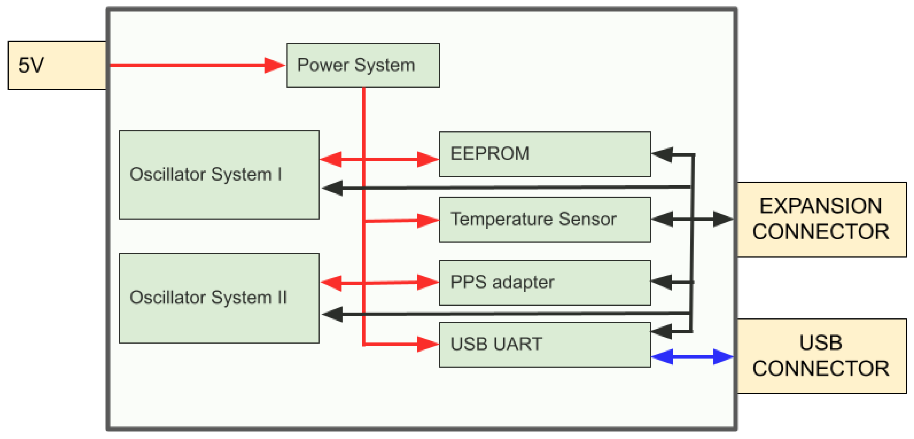
3. Architecture of the Expansion Board

The designed board includes all the WR hardware needed to successfully operate the protocol, with the exception of the FPGA. It is composed of six subsystems, which are the power supply subsystem; the one-wire temperature sensor; an electrically erasable programmable read-only memory (EEPROM); a pulse-per-second (PPS) adapter; a USB UART; and the oscillator subsystems. The architecture of the expansion board is displayed in Figure 2. Details about each subsystem follow:
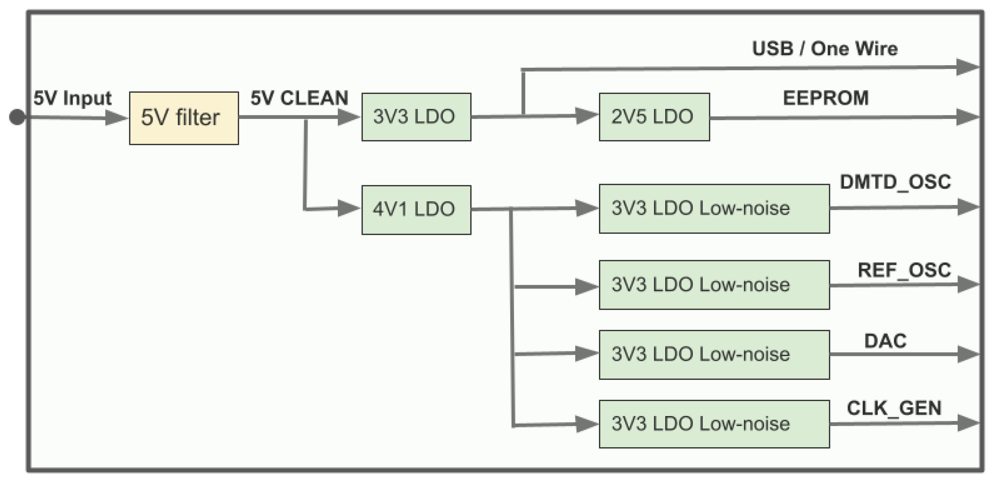
  • The power supply subsystem: This subsystem generates all the internal voltages needed. The expansion board is supplied at 5 V. The 5 V is cleaned from high-frequency noise by means of a ferrite bead and supplies the linear regulators where the power rail needed is generated. A 3.3 V voltage is generated, which is used for supplying a USB UART. The 3.3 V output feeds a linear and low-dropout (LDO) where the 2.5 V rail to supply the EEPROM is generated. In addition, the cleaned 5 V feeds another LDO to generate a 4.1 V rail, which is used, in turn, to supply four low-noise LDOs to generate the 3.3 V needed by the oscillator systems. The architecture of the power supply is shown in Figure 3. The low noise 3.3 V outputs are used as a reference by the oscillators, to supply the digital-to-analog converter (DAC), and to supply the secondary clock system. Each of the previous functions is achieved by means of independent rails.
  • One-wire temperature sensor, the medium access controller address provider: A one-wire [30] temperature sensor is included in the board. In addition, to provide temperature measurement, the identification number of this sensor is used to generate a unique medium access controller (MAC) [31] address for the protocol. The sensor is accessed with a one-wire interface.
  • Electrically erasable programmable read-only memory: An EEPROM allows for the storage of several configuration parameters of the protocol. It can be accessed via an I2C interface and can store the device’s configuration data, such as the MAC address.
  • Pulse-per-second adapter: An adapter of the PPS signal generated by the WR PTP Core is included in the expansion board. The PPS signal is an input of the expansion board, which adapts the signal for a SMA connector.
  • USB UART: A USB UART with a mini-USB connector has been included to provide access to the WR FPGA through the expansion board. This USB UART is particularly useful for outputting debug messages from the WRPC. The FPGA implementation of a regular UART is relatively simple and it can be connected to any modern computer through the bridge.
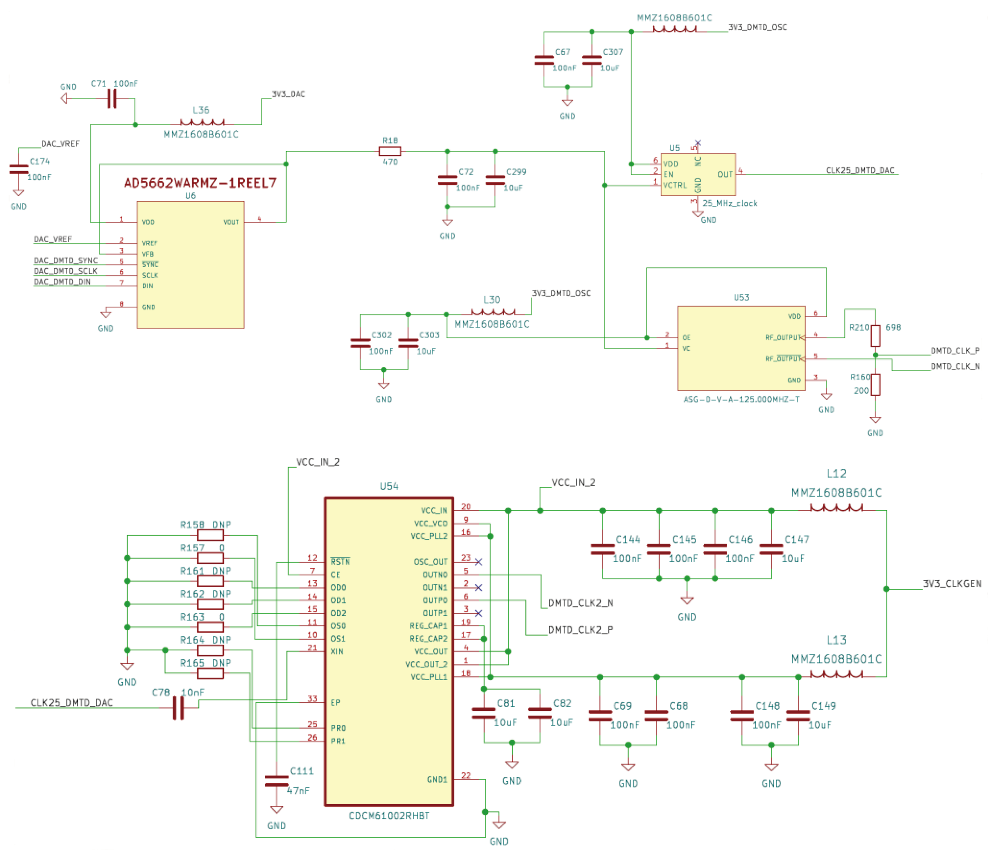
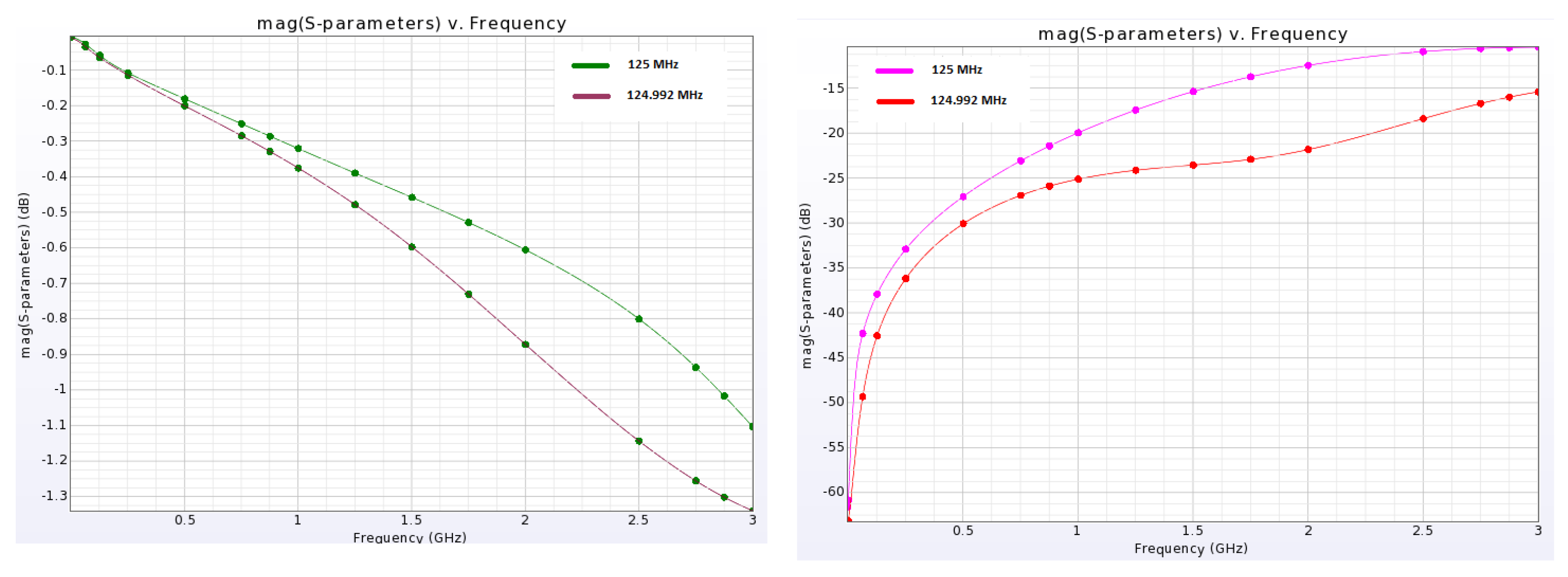
  • Oscillator subsystems: These two subsystems generate the clock needed by the WRPC DDMTD running at the FPGA for a precise measurement of the phase. The frequencies generated are 125 MHz and 124.992 MHz.
Figure 3. The power subsystem generates the necessary voltages from the 5 V input. The 5 V input is filtered and then fed to two LDOs, which generate the 3.3 V and 4.1 V voltages. The 3.3 V voltage is then fed to another LDO to obtain the 2.5 V voltage. The 4.1 V voltage is used to derive the 3.3 V outputs for operating the oscillator system, using four low-noise LDOs. To ensure a clean power supply and prevent interference, the 3.3 V low-noise rails have been isolated.
Electronics 12 03394 g003

3.1. Oscillator Subsystems

The main subsystem of the board is the clock generator. The WR protocol needs two clocks, one with a frequency of 125 MHz, and a second one with 124.992 MHz, which is the source of the offset frequency for DDMTD. These two clocks are generated by the expansion board in two different ways. The first one uses oscillators of that frequency, and the second one uses clock generators fed with oscillators of 25 MHz. The crystals that will generate the 125 MHz and 124.992 MHz frequencies are from Abracon. The noise phase for these oscillators is shown in Figure 4 and its rise and fall time are, as a maximum value, 3 ns. The second subsystem uses two crystals of 25 MHz, which supply two CDCM61002 clock generators. The phase jitter for these oscillators is 0.4 ps for an integration bandwidth from 12 kHz to 20 MHz. One creates the 125 MHz, while the other creates the 124.992 MHz clock signal. The crystal oscillators in both systems are supplied at 3.3 V. Two DAC provides the voltage control of the crystals. The output voltage of the DACs is controlled from the WRPC via an I2C bus, in order to lock the oscillators to the PLL (phase locked loop) of White Rabbit. The inclusion of the two subsystems will allow for their evaluation and comparison in real operation. The schematics of the two subsystems for the 125 MHz generation are shown in Figure 5. Prior to testing, it is expected that the subsystem using the quartz at the desired frequencies will have lower phase noise and achieve higher precision in synchronization, while the system using the 25 MHz quartz will be more cost-effective and simpler to manufacture. Future tests will determine the differences in terms of phase noise and synchronization.

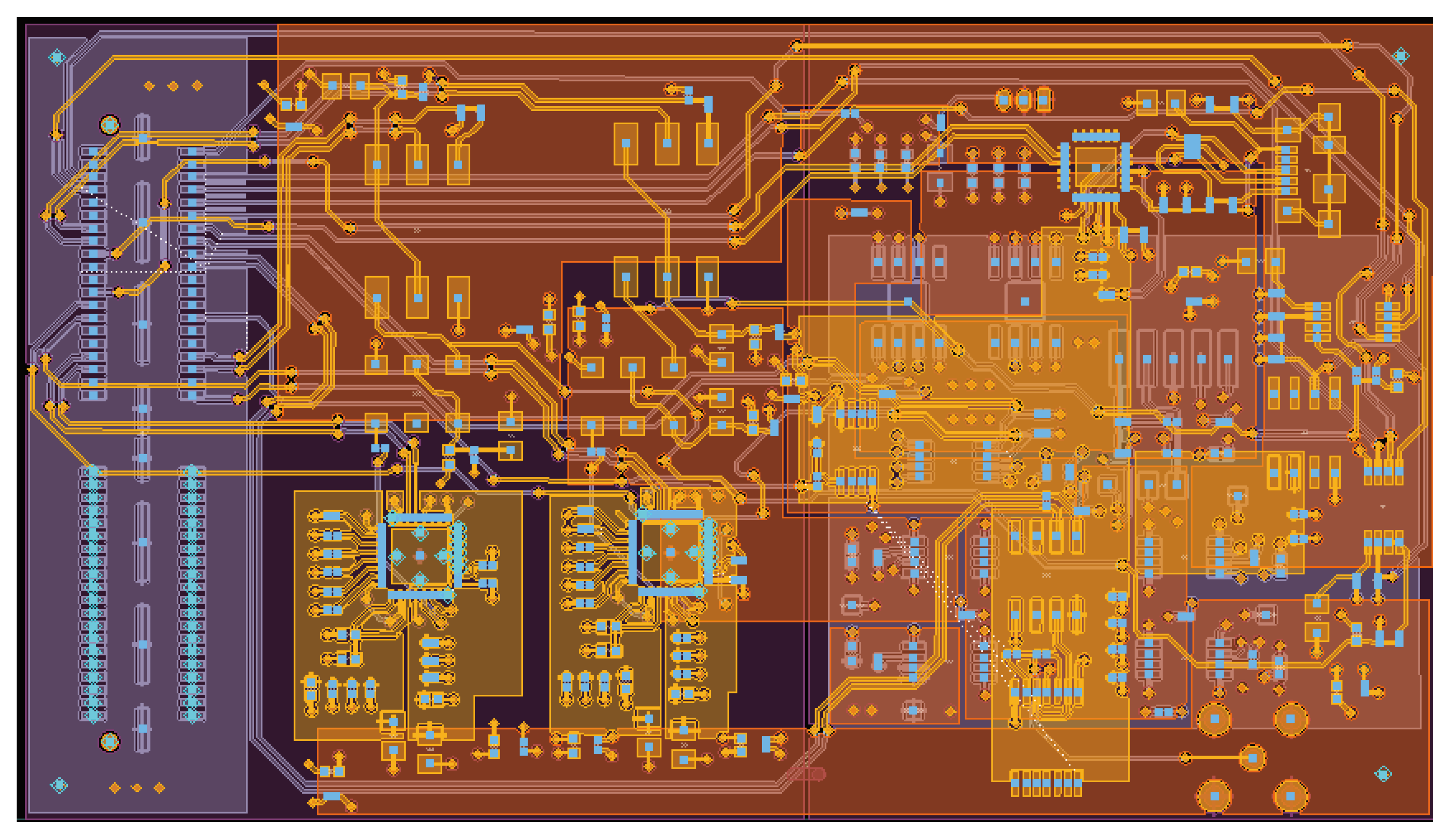
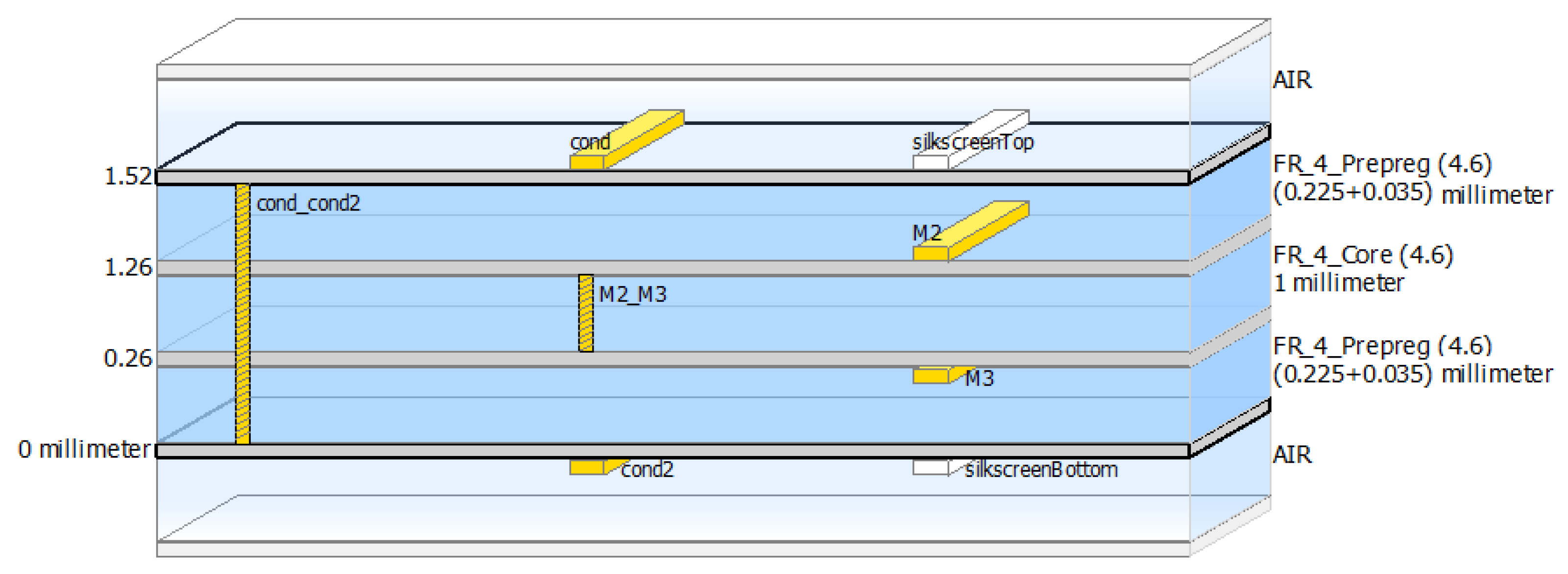
3.2. Printed Circuit Board Layout

The layout of the board has been made using four layers, two for signals, placed on the top and bottom layers, one for power planes, and one for ground. The layout of the board is shown in Figure 6, while the stackup is shown in Figure 7. The bottom of the board has no components. The oscillator signals are routed in the external layer as the dielectric constant of the air is lower than any of the dielectric materials in the PCB. In these layers, the signal propagation speed is higher, and, therefore, the attenuation is lower [32]. An important characteristic to obtain precise synchronization is the phase noise of the clocks. The transmission of clock signals across a printed circuit board (PCB) degrades by a variety of factors, such as channel losses, cross-talk noise, power noise, or reflection noise [33]. The frequency-dependent losses of the transmission line have a significant impact on signal quality and timing, resulting in an increase in jitter [34]. Additionally, the stability of supply voltage, or the layout of the tracks, will affect the figure of noise. To try to reduce these effects, an isolated ground area dedicated solely to the components of the clock system has been created. To limit insertion losses for both package and board, routing length has been kept as low as possible. Separated power distribution networks (PDN) have been used for the reference clocks, the DDMTD clocks, and the DACs. The PDN has been designed to minimize its impedance, as it directly impacts noise generation.

4. Power and Signal Integrity Analysis

4.1. Previous Developments and Justification of Virtual Prototyping

A daughter board was designed to provide White Rabbit capabilities to the Pixie-Net XL board [35]. The expansion board designed included two VCOs, and achieved an overall jitter of 300 ps. A redesign of the clock circuitry was made in order to improve the jitter but it was unsuccessful.
Virtual prototyping [36,37,38,39] can be used to verify the behavior of the PCB before its production, being able to identify possible design flaws, signal integrity issues, and electrical performance problems in an early stage and introduce the necessary modifications before the manufacturing of the first prototypes avoiding expensive physical iterations [40,41,42]. The use of advanced tools to simulate the PCB layout has the advantage of reducing the design cycle since it is not necessary to have a real prototype.
In our case, the track width of the oscillator signal and the via architecture were optimized before the layout was implemented. Once the layout was completed, the PDN of the oscillator system and the signal attenuation of the clock signals were analyzed to validate the design through simulations before starting its manufacturing.

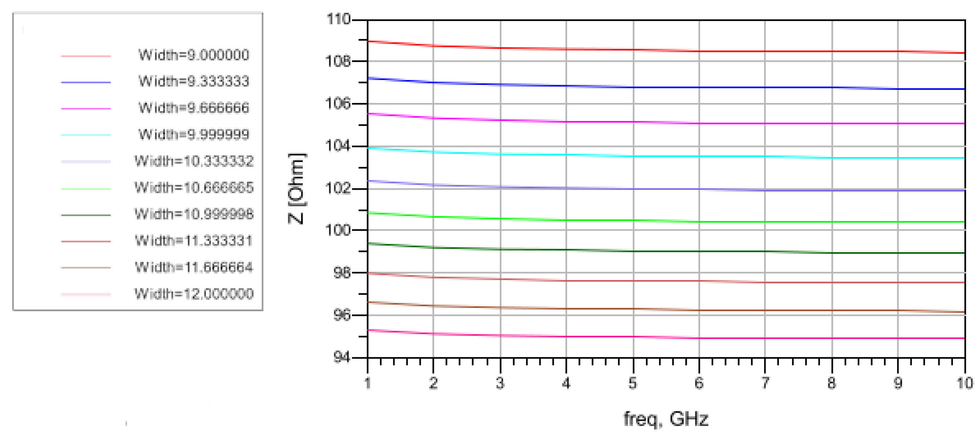
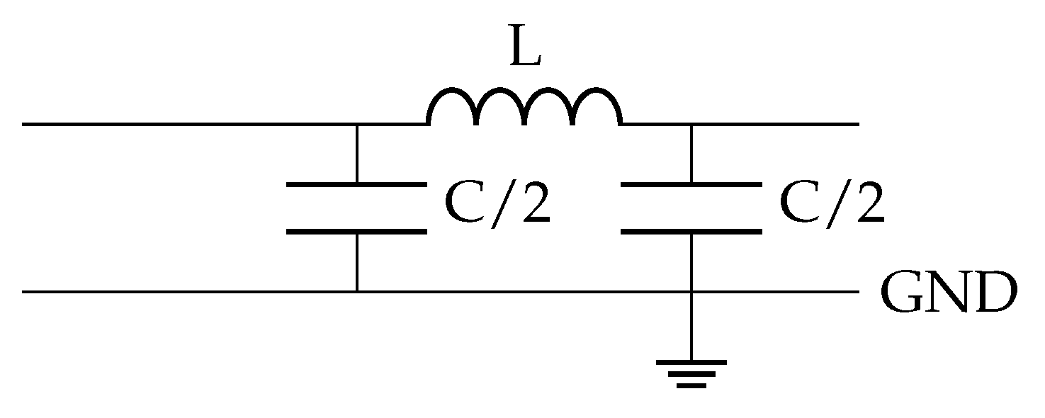
4.2. Pre-layout Signal Integrity Simulations

The most critical signals on the board in terms of signal integrity are the oscillator system signals since they determine synchronization. The clock signals are transmitted using LVDS (low-voltage differential signals). A track geometry has been designed to maintain a characteristic impedance of 100 Ω. For the non-differential signals, geometry has been designed to maintain a characteristic impedance of 50 Ω. These geometries have been simulated using PathWave Advance Design System (ADS) 2020 from Keysight [43,44]. For the differential lines, a separation of 0.25 mm has been set in external tracks. Furthermore, a simulation has been performed to determine the optimal track width to maintain the characteristic impedance for both differential and single tracks. An optimal width of 0.27 mm results from the simulations (See Figure 8). The connections between tracks of different layers through pathways can generate negative effects that affect the integrity of the signal [45]. When using a via, all layers of the electronic board are perforated. In the layers where it connects with the tracks, a copper zone is generated around the hole called pad and in those layers where there is no connection, a copper-free zone is generated that surrounds the perforation. This copper-free zone is called antipad. This structure carries implicit parasitic capacitances and inductances that generate discontinuities affecting the integrity of the signal. The model equivalent of the via is shown in Figure 9. In this model, the parasitic capacitance and the inductance are defined by the following equations:
C ( p F ) = ε r 2 D p a d × l υ D a n t i p a d D p a d
L ( n H ) = 5.08 × l υ ln 4 × l υ d υ + 1
where ε r is the dielectric constant, D p a d and D a n t i p a d are the diameters of the pads and antipads, l υ is the length of the via, and d υ is the diameter of the via hole, all expressed in inches. This model creates a low-pass filter, where the cutoff frequency is determined by the values of L and C. To mitigate the effects caused by vias, efforts will be made to reduce parasitic capacitance by increasing the diameter of the antipad. To minimize the impact of parasitic inductance, return vias can be used, connected to the ground planes.
A simulation has been carried out modeling the differential vias. The model created is shown in Figure 10. For this model, the diameter of the antipad has been varied, from 0.7 mm to 1.5 mm. It is observed how the smallest impedance discontinuity is obtained for an antipad diameter of 1.5 mm.

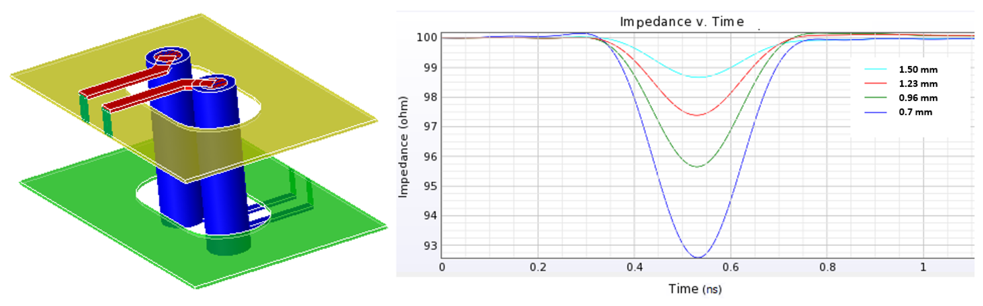
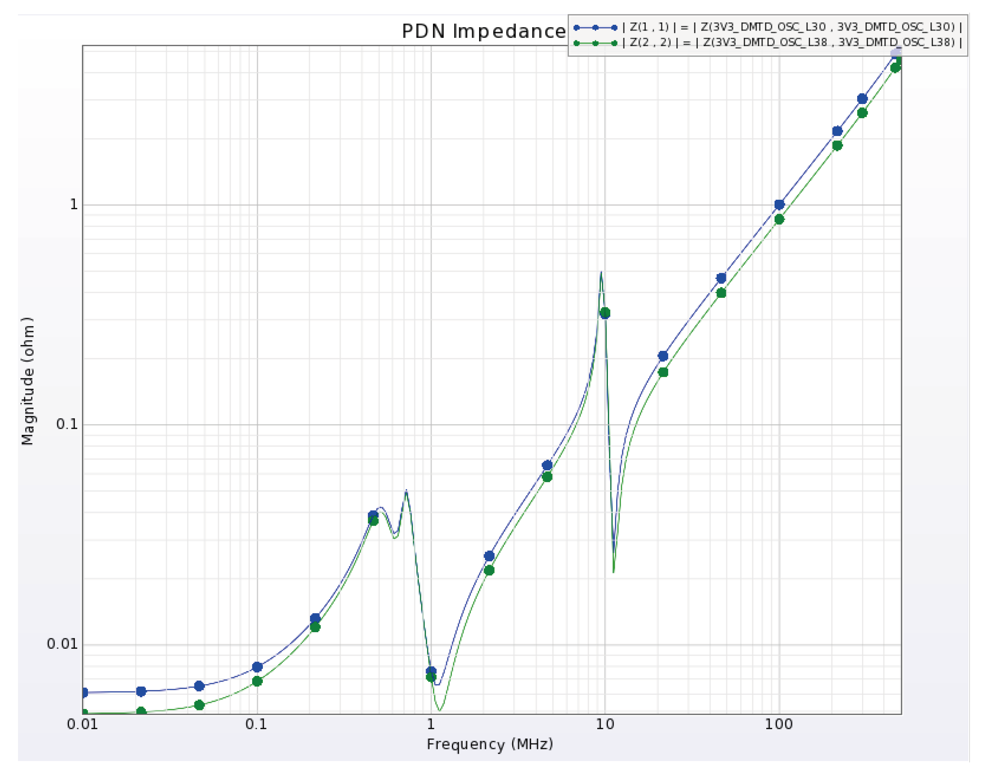
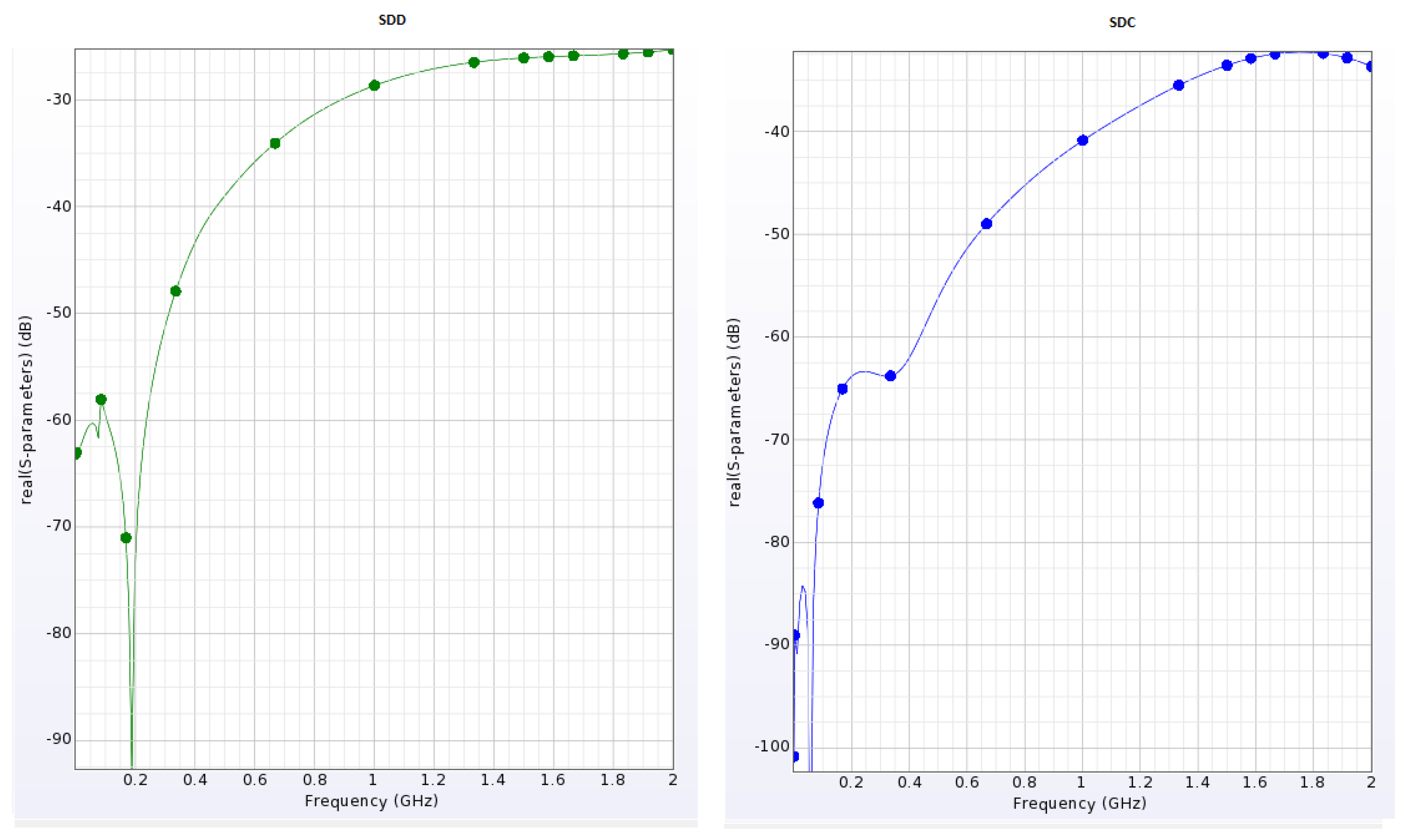
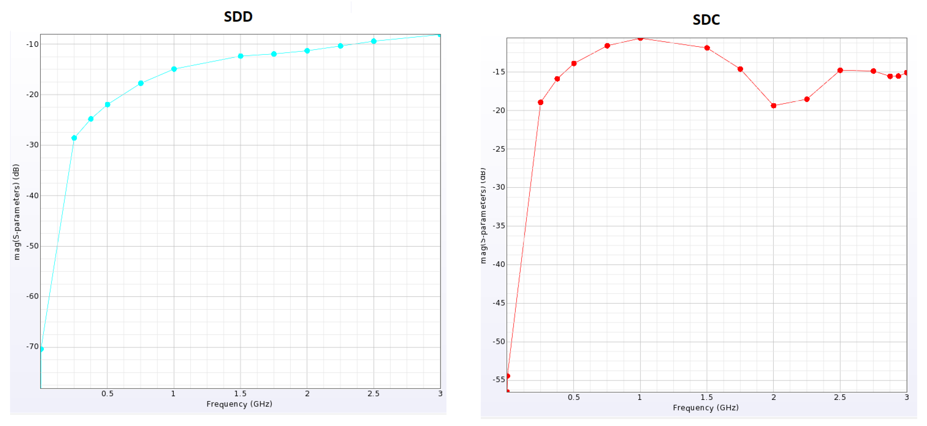
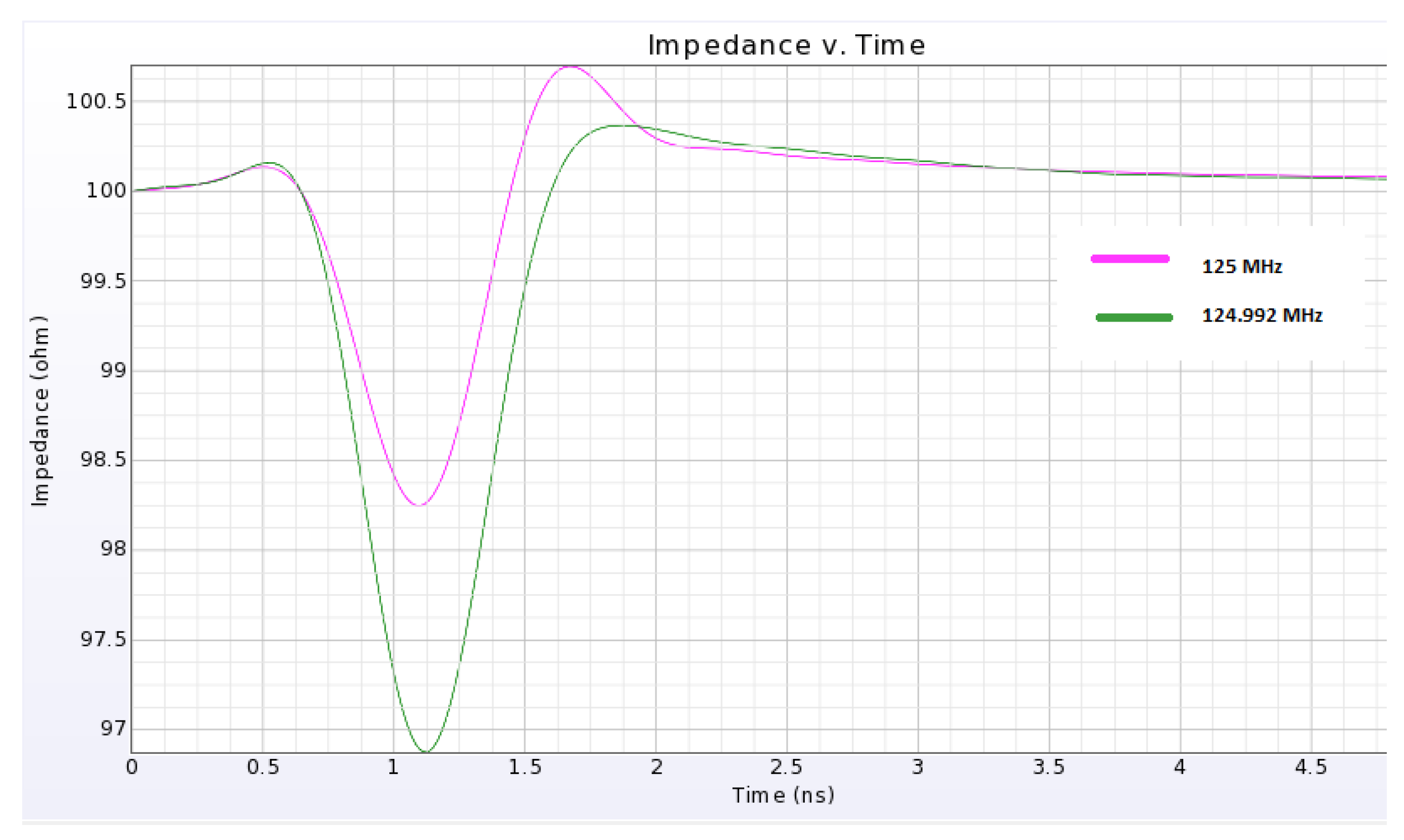
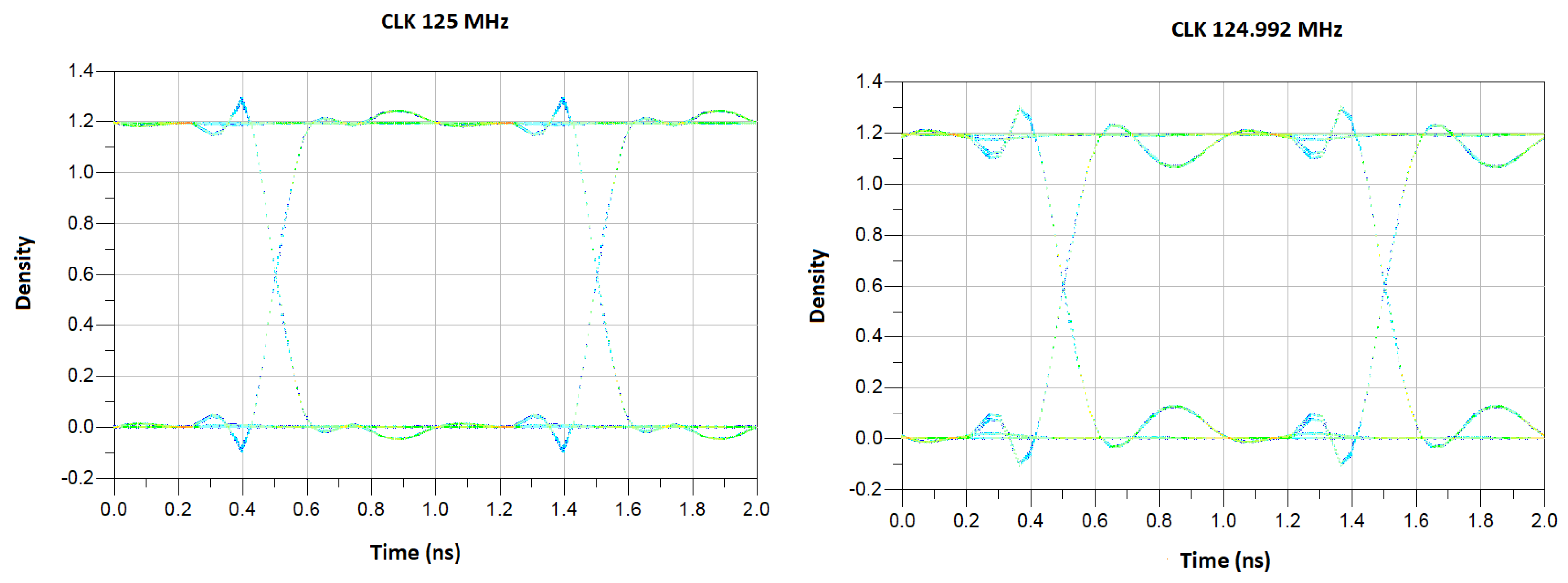
4.3. Post-layout Power and Signal Integrity Simulations

It is important to keep PDN impedance on the PCB as low as possible to minimize the simultaneous switching noise (SSN). This is critical in the case of the oscillator system, as the noise in the PDN will result in a jitter in the clock system. Any transient current in the PDN causes SSN [46]. The level of the SSN generated is directly related to the impedance of the PDN. The noise is induced by the power rail and contributes to the appearance of jitter in the signals generated by the elements supplied for that PDN. The peak-to-peak voltage of the SSN is given by Equation (5) [47]:
V S S N p p = I × Z P D N
where V S S N p p is the SSN on a particular power rail; I is the transient current circulating in the PDN; and Z P D N is the impedance of the PDN.
The impedance of the PDNs has been simulated using ADS, where the capacitors employed to reduce the impedance have been optimized. The desired impedance value has been set to 1 Ω at 100 MHz. The bandwidth of a step current change, corresponding to a specific rise time, is determined by the equation:
BW = 0.35 rise time
For the current scenario, with a rise time of 3 ns, the resulting bandwidth (BW) is calculated as 116.7 MHz. The oscillators operate within the voltage range of 3.135 to 3.465 V. The maximum ripple achieved while adhering to the target impedance is approximately 0.035 V, equivalent to around 1% of the amplitude, comfortably below the oscillators’ operational range. The same conclusion can be reached assuming a very conservative ripple of the current of 20 mA. At the most unfavorable case (Vi = 3.135 V) and with a voltage ripple of 1%, the impedance obtained using Equation (5) is 1.57 Ω. The result of the simulation of the PDN for the power rail of the DDMTD clock generator is shown in Figure 11.
The lines that are most critical to signal integrity are those related to the oscillator system. There are various factors that can cause signal quality degradation, including connectors, dielectric materials, capacitors, encapsulated components, and board and trace design and geometry. One method to analyze signal integrity is through the use of scattering parameters or S-parameters [48]. This technique models interconnections as two-port networks in the frequency domain, representing the relationships between incoming and outgoing waves. Figure 12 depicts a representation of these networks, where ports 1 and 4 represent the incident waves, and ports 2 and 3 represent the outgoing waves. Based on this representation and nomenclature, the S-parameters are defined according to the relationship:
s k j = O u t p u t w a v e a t p o r t k ( V ) I n p u t w a v e a t p o r t j ( V )
Therefore, parameter S 11 refers to the relationship between an incoming wave through port 1 and the wave reflected back from the same port, while parameter S 21 refers to the relationship between an incoming wave through port 1 and the wave exiting from port 2. Figure 13 illustrates both of these relationships. The parameter S 11 in an interconnection evaluates the amount of signal that will be reflected by that interconnection. This reflection occurs due to impedance mismatch in the interconnection and can be quantified by the reflection coefficient, as indicated in the following expression:
S 11 ( d B ) = 20 × log Z L Z o Z L + Z o
where the term Z L refers to the load impedance, and the term Z o refers to the characteristic impedance. Parameter S 21 on the other hand pertains to insertion loss. It measures the amount of signal loss experienced along the path from the input port to the output port. These losses can also arise from impedance mismatch. The longer the mismatch region, the greater the losses will be. In the case of good matching, the dominant term for insertion losses would be those caused by the dielectric. Without accounting for losses due to coupling to adjacent traces, conductor losses, or losses from radiated emissions, the conservation of energy establishes a relationship between the S 11 and S 21 parameters as shown below:
S 11 2 + S 21 2 = 1 S 21 = 1 S 11 2
The same relationship of S-parameters can also be applied to differential lines, where the ports themselves are differential ports. The use of differential ports gives rise to signal conversion between differential and common modes, leading to the creation of the so-called mixed S-parameter matrix. Table 1 illustrates the representation of the mixed matrix for two differential ports. The SDD parameters refer to ports where the signal enters and exits in differential mode, SCC refers to the signal entering and exiting the ports in common mode, and the terms SDC and SCD refer to signals entering through one port in common mode and exiting through the other in differential mode, and vice versa.
Following the same nomenclature as in Equation (7), the parameter S C D 21 refers to the ratio of differential signal that enters through port 1 and exits through port 2 in common mode, whereas the term S D D 21 pertains to the ratio of signal that enters through port 1 and exits through port 2 in differential mode.
Under these parameters, the insertion and return losses of the clock lines were simulated with the rise (and fall) time set to 1 ns. Figure 14 displays the insertion losses in the clock differential lines, where low insertion losses guarantee low jitter and high synchronization. Another potential source of noise that can affect signal integrity is coupling, where parasitic capacitances between traces or tracks create induced voltages and produce noise in adjacent tracks. These tracks, referred to as victims, will have two noise components: one at their opposite end, known as FEXT (far-end crosstalk), and another at their near end, called NEXT (near-end crosstalk) [49]. These effects have been simulated in the traces of two differential pairs corresponding to the lines of the clocks, as they are the closest to each other. All the clock lines are routed with the same separation, so simulating two of them is sufficient to validate the design. Figure 15 and Figure 16 show the results of simulations of induced noise NEXT and FEXT in differential mode to differential mode (parameter SDD) and in differential mode to common mode (parameter SCD) between two differential clock tracks. These figures show that the coupled noise, around −40 dB, is very low and will not affect the integrity of the signals. In addition, a simulation of the characteristic impedances of the differential pairs of the clock lines has been performed. All of them were designed with an appropriate topology to maintain a characteristic impedance of 100 Ω. The differential pairs of the greatest length were simulated. Figure 17 shows the simulation results, indicating that a variation greater than ±6% is not exceeded, which is an acceptable variation. The pronounced peaks appearing in the simulation are capacitive effects due to the perforations or vias at the ends of the connection. The simulation results align with the pre-layout analysis, the results of which are presented in Figure 11.
To verify that clock line fluctuations will not introduce additional jitter, an eye diagram simulation has been performed. Figure 18 shows the results of the eye diagrams obtained for clock differential lines. Based on the diagram, a detailed study of fluctuations or jitter has been conducted. The total jitter observed is caused by two main components: random and deterministic [50,51]. Random fluctuations (random jitter—RJ) are produced by noise sources such as transmitter clock phase noise or intrinsic noise such as thermal noise. They are not related to any signal in the system and follow a Gaussian distribution. As it is a Gaussian distribution, the most appropriate way to express it is in terms of standard deviation or root mean square (RMS). Deterministic fluctuations occur when working with components that are not ideal. They are repetitive fluctuations that are predictable and can be classified into several types:
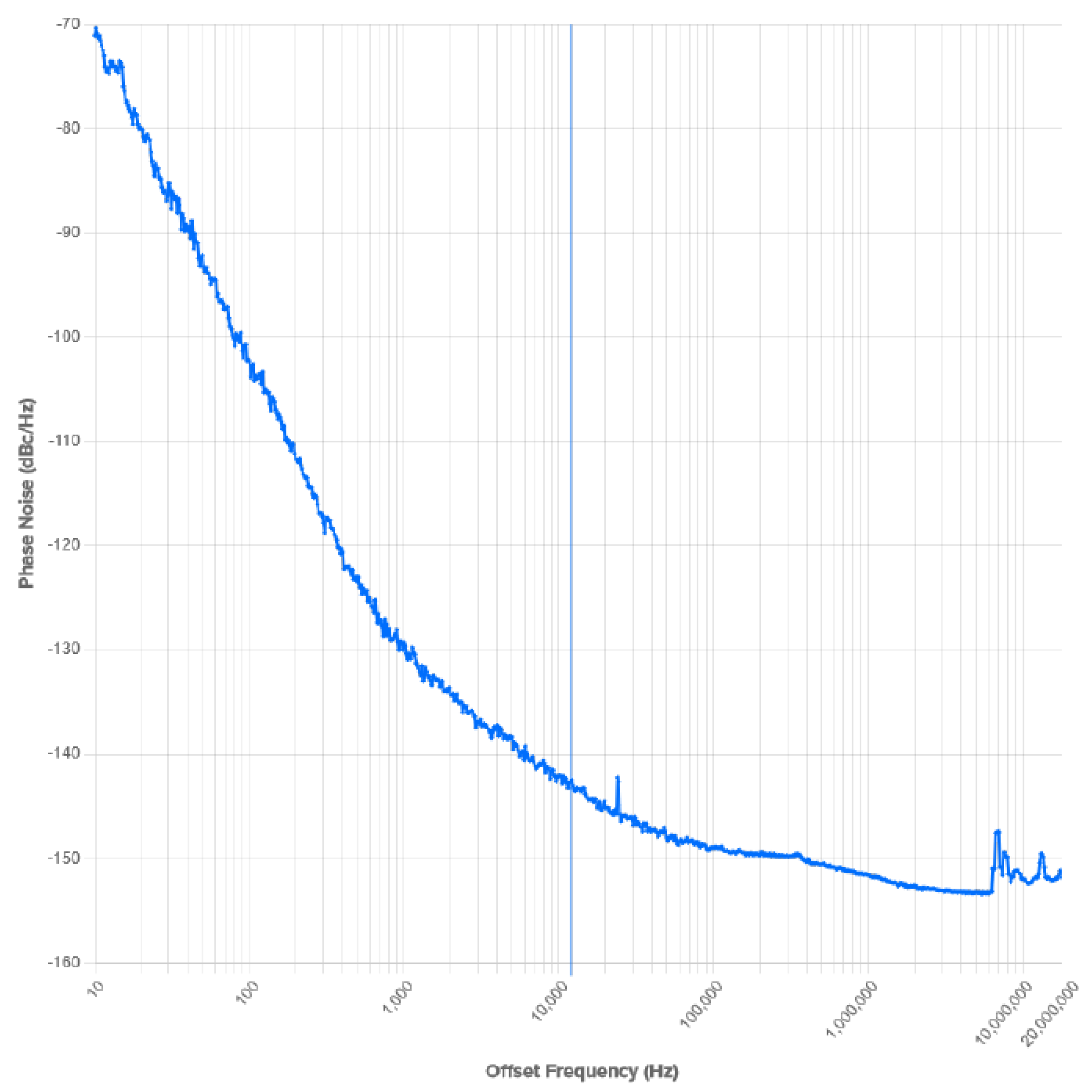
  • Inter symbol interference (ISI), produced by the interference of one bit with the next or due to reflections.
  • Duty cycle distortion (DCD), produced by alterations in the symmetry of the rising and falling edges, generating a distortion figure with two peaks.
  • Periodic jitter (PJ), generated by coupling, noise on power rails, noise on substrates, or instabilities in feedback loops.
Table 2 shows the contributions to the observed fluctuations in the 125 MHz and 124.992 MHz lines of the first oscillator system. The low jitter values obtained, along with the opening of the eye diagram, ensure the required level of synchronization.

5. Conclusions and Future Work

The White Rabbit protocol requires special hardware to operate. In this work, the design and architecture of an expansion board that includes the hardware required by the protocol, which is not usually available on FPGA boards, has been presented. The expansion board adds flexibility by including two different oscillator systems. Additionally, the signal integrity analysis performed on the expansion board is presented. The signal integrity results predict that the phase noise of the oscillator will be acceptable, and therefore the obtained synchronization will be of the subnanosecond order. The next steps will include manufacturing the board and testing both oscillator systems in a White Rabbit network.

Author Contributions

Conceptualization, D.R. and D.C.; methodology, D.R.; software, D.C. and M.M; validation, D.C., M.M. and D.R.; formal analysis, J.d.D.Z. and D.R.; investigation, D.R.; resources, D.R. and J.d.D.Z.; data curation, D.C.; writing—original draft preparation, D.R.; writing—review and editing, D.R.; visualization, D.C.; supervision, J.d.D.Z.; project administration, D.R. and J.d.D.Z.; funding acquisition, J.d.D.Z. and D.R. All authors have read and agreed to the published version of the manuscript.

Funding

This research was funded by the financial support of the Ministerio de Ciencia e Innovación: Programa Estatal para Impulsar la Investigación Científico-Técnica y su Transferencia (refs. PID2021-124591NB-B-C41) (MCIU/FEDER), Programa de Planes Complementarios I+D+I (refs. ASFAE/2022/023), Generalitat Valenciana: Prometeo (PROMETEO/2020/019), Grisolía (ref. GRISOLIAP/2021/192) and GenT (refs. CIDEGENT/2018/034, /2020/049, /2021/23) programs, EU: MSC program (ref. 101025085), Spain.

Data Availability Statement

The data presented in this study are available on request from the corresponding author. The data are not publicly available due to be in a local repository.

Conflicts of Interest

The authors declare no conflict of interest.

References

  1. IEEE Std 1588-2019; Synchronization Distribution in 5G Transport Networks. (Revision of IEEE Std 1588-2008). IEEE: Manhattan, NY, USA, 2022.
  2. Venmani, D.; Lagadec, Y.; Lemoult, O.; Deletre, F. Phase and Time Synchronization for 5G C-RAN: Requirements, Design Challenges and Recent Advances in Standardization. EAI Endorsed Trans. Ind. Netw. Intell. Syst. 2018, 5, 155238. [Google Scholar] [CrossRef]
  3. Li, H.; Han, L.; Duan, R.; Garner, G.M. Analysis of the Synchronization Requirements of 5 g and Corresponding Solutions. IEEE Commun. Stand. Mag. 2017, 1, 52–58. [Google Scholar] [CrossRef]
  4. Geng, Y.; Liu, S.; Yin, Z.; Naik, A.; Prabhakar, B.; Rosenblum, M.; Vahdat, A. Exploiting a Natural Network Effect for Scalable, Fine-grained Clock Synchronization. In Proceedings of the Symposium on Networked Systems Design and Implementation, Renton, WA, USA, 9–11 April 2018. [Google Scholar]
  5. Ageron, M.; Aguilar, J.A.; Al Samarai, I.; Albert, A.; Ameli, F.; André, M.; Anghinolfi, M.; Anton, G.; Anvar, S.; Ardid, M.; et al. ANTARES: The first undersea neutrino telescope. Nucl. Instrum. Meth. A 2011, 656, 11–38. [Google Scholar] [CrossRef]
  6. Adrian-Martinez, S.; Ageron, M.; Aharonian, F.; Aiello, S.; Albert, A.; Ameli, F.; Anassontzis, E.; Andre, M.; Androulakis, G.; Anghinolfi, M.; et al. Letter of intent for KM3NeT 2.0. J. Phys. G 2016, 43, 084001. [Google Scholar] [CrossRef]
  7. Aartsen, M.G.; Ackermann, M.; Adams, J.; Aguilar, J.A.; Ahlers, M.; Ahrens, M.; Altmann, D.; Andeen, K.; Anderson, T.; Ansseau, I.; et al. The IceCube Neutrino Observatory: Instrumentation and Online Systems. J. Instrum. 2017, 12, P03012. [Google Scholar] [CrossRef] [Green Version]
  8. Andres, E.; Askebjer, P.; Barwick, S.W.; Bay, R.; Bergström, L.; Biron, A.; Booth, J.; Bouchta, A.; Carius, S.; Carlson, M.; et al. The AMANDA neutrino telescope: Principle of operation and first results. Astropart. Phys. 2000, 13, 1–20. [Google Scholar] [CrossRef] [Green Version]
  9. Malyshkin, Y. Baikal-GVD neutrino telescope: Design reference 2022. Nucl. Instrum. Meth. A 2023, 1050, 168117. [Google Scholar] [CrossRef]
  10. Perlin, M. Particle Physics with the Pierre Auger Observatory. SciPost Phys. Proc. 2022, 8, 130. [Google Scholar] [CrossRef]
  11. Terzian, Y.; Lazio, J. The Square Kilometre Array. Proc. SPIE Int. Soc. Opt. Eng. 2006, 6267, 62672D. [Google Scholar] [CrossRef] [Green Version]
  12. Ferrini, F.; Wild, W. The Cherenkov Telescope Array Observatory Comes of Age. ESO Messenger 2020, 180, 3–8. [Google Scholar] [CrossRef]
  13. Lipinski, M.; Wlostowski, T.; Serrano, J.; Alvarez, P. White rabbit: A PTP application for robust sub-nanosecond synchronization. In Proceedings of the 2011 IEEE International Symposium on Precision Clock Synchronization for Measurement, Control and Communication, Munich, Germany, 12–16 September 2011; pp. 25–30. [Google Scholar] [CrossRef]
  14. White Rabbit PTP Core. Available online: https://ohwr.org/projects/wr-cores/wiki/wrpc-core (accessed on 28 February 2012).
  15. White Rabbit Collaboration. Available online: https://www.white-rabbit.tech/ (accessed on 28 February 2012).
  16. Serrano, J.; Alvarez, P.; Cattin, M.; Garcia Cota, E.; Lewis, J.; Moreira, P.; Wlostowski, T.; Gaderer, G.; Loschmidt, P.; Dedic, J.; et al. White Rabbit Project. In Proceedings of the ICALEPCS2009, Kobe, Japan, 12–16 October 2009; pp. 93–95. [Google Scholar]
  17. IEEE Std 1588-2008; IEEE Standard for a Precision Clock Synchronization Protocol for Networked Measurement and Control Systems. Revision of IEEE Std 1588-2002). IEEE: Manhattan, NY, USA, 2008; pp. 1–269. [CrossRef]
  18. Lan, Y.K.; Chen, Y.S.; Hou, T.C.; Wu, B.L.; Chu, Y.S. Development Board Implementation and Chip Design of IEEE 1588 Clock Synchronization System Applied to Computer Networking. Electronics 2023, 12, 2166. [Google Scholar] [CrossRef]
  19. Timing Characteristics of Synchronous Ethernet Equipment Slave Clock: G.8262/Y.1362 International Telecommunication Union. 2010. Available online: https://www.itu.int/rec/dologin_pub.asp?lang=e&id=T-REC-G.8262-201007-S!!PDF-E&type=items (accessed on 7 August 2023).
  20. IEEE Std 1588-2019; IEEE Standard for a Precision Clock Synchronization Protocol for Networked Measurement and Control Systems. (Revision ofIEEE Std 1588-2008). IEEE: Manhattan, NY, USA, 2020; pp. 1–499. [CrossRef]
  21. Li, F.; Liu, W.; Qi, Y.; Li, Q.; Liu, G. An Enhanced Method for Nanosecond Time Synchronization in IEEE 1588 Precision Time Protocol. Processes 2023, 11, 1328. [Google Scholar] [CrossRef]
  22. Bielewicz, M.; Bancer, A.; Dziedzic, A.; Grzyb, J.; Jaworska, E.; Kasprowicz, G.; Kiecana, M.; Kolasinski, P.; Kuc, M.; Kuklewski, M.; et al. Practical Implementation of an Analogue and Digital Electronics System for a Modular Cosmic Ray Detector—MCORD. Electronics 2023, 12, 1492. [Google Scholar] [CrossRef]
  23. Aiello, S.; Ameli, F.; Andre, M.; Androulakis, G.; Anghinolfi, M.; Anton, G.; Marinelli, A.; Anton, G.; Ardid, M.; Markou, C.; et al. KM3NeT front-end and readout electronics system: Hardware, firmware and software. J. Astron. Telesc. Instrum. Syst. 2019, 5, 046001. [Google Scholar] [CrossRef] [Green Version]
  24. Vella Wallbank, J.; Amodeo, M.; Beaumont, A.; Buzio, M.; Di Capua, V.; Grech, C.; Sammut, N.; Giloteaux, D. Development of a Real-Time Magnetic Field Measurement System for Synchrotron Control. Electronics 2021, 10, 2140. [Google Scholar] [CrossRef]
  25. Jones, T.; Arnold, D.; Tuffner, F.; Cummings, R.; Lee, K. Recent Advances in Precision Clock Synchronization Protocols for Power Grid Control Systems. Energies 2021, 14, 5303. [Google Scholar] [CrossRef]
  26. Nabwani, M.; Suleymanov, M.; Pinhasi, Y.; Yahalom, A. Real-Time Fault Location Using the Retardation Method. Electronics 2022, 11, 980. [Google Scholar] [CrossRef]
  27. Rifandi, R.; Assagaf, S.; Ningtyas, Y.D.W.K. An Insight about GPS; Utrecht University Summer School: Utrecht, The Netherlands, 2013. [Google Scholar] [CrossRef]
  28. Lee, J. Global Positioning/GPS. Int. Encycl. Hum. Geogr. 2009, 68, 548–555. [Google Scholar] [CrossRef]
  29. Moreira, P.; Alvarez, P.; Serrano, J.; Darwezeh, I.; Wlostowski, T. Digital dual mixer time difference for sub-nanosecond time synchronization in Ethernet. In Proceedings of the 2010 IEEE International Frequency Control Symposium, Newport Beach, CA, USA, 1–4 June 2010; pp. 449–453. [Google Scholar] [CrossRef]
  30. Overview of 1-Wire Technology and Its Use. Available online: https://www.analog.com/en/technical-articles/guide-to-1wire-communication.html (accessed on 28 February 2012).
  31. IEEE Std 802.3-2002; IEEE Standard for Information Technology-Telecommunications and Information Exchange between Systems-Local and Metropolitan Area Networks-Specific Requirements Part 3: Carrier Sense Multiple Access with Collision Detection (CSMA/CD) Access Method and Physical Layer Specifications. (Revision of IEEE Std 802.3, 2000 edn). IEEE: Manhattan, NY, USA, 2002; pp. 1–1550. [CrossRef]
  32. Thierauf, S. High-Speed Circuit Board Signal Integrity; Artech House Microwave Library, Artech House: Norwood, MA, USA, 2004. [Google Scholar]
  33. Chang, K.K.; nan Kuo, C.; Wu, T.L.; Chen, W.L.; Wu, R.B. Equivalent circuit of a through via in multi-layer environment. In Proceedings of the Electrical Performance of Electronic Packaging, Pittsburgh, PA, USA, 22–24 April 1992; pp. 59–61. [Google Scholar] [CrossRef]
  34. Siebert, K.; Gunther, H.; Frei, S.; Mickisch, W. Modeling of Frequency Dependent Losses of Transmission Lines with VHDL-AMS in Time Domain. In Proceedings of the 2009 20th International Zurich Symposium on Electromagnetic Compatibility, Zurich, Switzerland, 12–16 January 2009; pp. 313–316. [Google Scholar] [CrossRef]
  35. Hennig, W.; Hoover, S. White Rabbit Time Synchronization for Radiation Detector Readout Electronics. IEEE Trans. Nucl. Sci. 2020, 68, 2059–2065. [Google Scholar] [CrossRef]
  36. Rogers, B.M. Virtual prototyping and concurrent engineering in PCB manufacturing. IEEE Trans. Electron. Packag. Manuf. 1997, 20, 300–308. [Google Scholar] [CrossRef]
  37. Zainudeen, P.B.; Althari, A.; Iqbal, M.T. A survey on virtual prototyping tools for PCB design. In Proceedings of the 2018 International Conference on Innovative Trends in Computer Engineering (ITCE), Aswan, Egypt, 19–21 February 2018; pp. 93–98. [Google Scholar] [CrossRef]
  38. Muir, D.; Panicker, R. The use of virtual prototyping in PCB design. In Proceedings of the 2015 IEEE MTT-S International Microwave Workshop Series on Advanced Materials and Processes for RF and THz Applications (IMWS-AMP), Suzhou, China, 1–3 July 2015; pp. 1–3. [Google Scholar] [CrossRef]
  39. Chen, J.Y.; Liu, K.S.; Huang, C.M. Virtual prototyping for signal integrity analysis of high-speed PCBs. IEEE Trans. Electromagn. Compat. 2006, 48, 711–720. [Google Scholar] [CrossRef]
  40. Silaghi, A.M.; Pescari, C.; Bleoju, C.; De Sabata, A. Solving Automotive Signal Integrity Issues by EMC Simulation. In Proceedings of the 2021 IEEE 27th International Symposium for Design and Technology in Electronic Packaging (SIITME), Timisoara, Romania, 25–30 October 2021; pp. 33–36. [Google Scholar] [CrossRef]
  41. Silaghi, A.M.; Mueller, F.; De Sabata, A.; Buta, A.P.; Nicolae, P.M. Analysis of Shielding Effectiveness of an Automotive Display through Simulation and Testing. In Proceedings of the 2020 International Symposium on Electromagnetic Compatibility-EMC EUROPE, Rome, Italy, 23–25 September 2020; pp. 1–4. [Google Scholar]
  42. Silaghi, A.M.; De Sabata, A. EMC Simulation of an Automotive Ethernet Interface. In Proceedings of the 2020 International Symposium on Electronics and Telecommunications (ISETC), Timisoara, Romania, 5–6 November 2020; pp. 1–4. [Google Scholar]
  43. Behagi, A. RF and Microwave Circuit Design: A Design Approach Using (ADS); Advanced Design System; Techno Search: Thane, India, 2015. [Google Scholar]
  44. Behagi, A. 100 RF and Microwave Circuit Design: With Keysight (ADS) Solutions; Techno Search: Thane, India, 2018. [Google Scholar]
  45. Johnson, H.; Graham, M. High-speed Digital Design: A Handbook of Black Magic; Prentice Hall Modern Semiconductor Design; Prentice Hall: Upper Saddle River, NJ, USA, 1993. [Google Scholar]
  46. Carrió, F.; Gonzalez, V.; Sanchis, E. Basic Concepts of Power Distribution Network Design for High-Speed Transmission. Open Opt. J. 2011, 5, 51–61. [Google Scholar] [CrossRef] [Green Version]
  47. Yee, C.F. Achieving Minimal PDN Impedance, SSN and Jitter on PCB with Embedded Capacitance Material. In Proceedings of the 2018 IEEE International RF and Microwave Conference (RFM), Penang, Malaysia, 17–19 December 2018; pp. 155–158. [Google Scholar] [CrossRef]
  48. Bogatin, E. Signal and Power Integrity–Simplified; Prentice Hall PTR Signal Integrity Library, Prentice Hall: Upper Saddle River, NJ, USA, 2010. [Google Scholar]
  49. Mudavath, R.; Naik, B.R. Estimation of Far End Crosstalk and Near End Crosstalk Noise with Mutually Coupled RLC Interconnect Models. In Proceedings of the 2018 International Conference on Communication and Signal Processing (ICCSP), Melmaruvathur, India, 3–5 April 2018; pp. 182–185. [Google Scholar] [CrossRef]
  50. Dou, Q.; Abraham, J.A. Jitter Decomposition in High-Speed Communication Systems. In Proceedings of the 2008 13th European Test Symposium, Verbania, Italy, 25–29 May 2008; pp. 157–162. [Google Scholar] [CrossRef]
  51. Ren, N.; Fu, Z.; Lei, S.; Liu, H.; Tian, S. Methodology for Digital Synthesis of Deterministic and Random Jitter Generation on Rising or Falling Edges of Data Pattern. Electronics 2019, 8, 1510. [Google Scholar] [CrossRef]
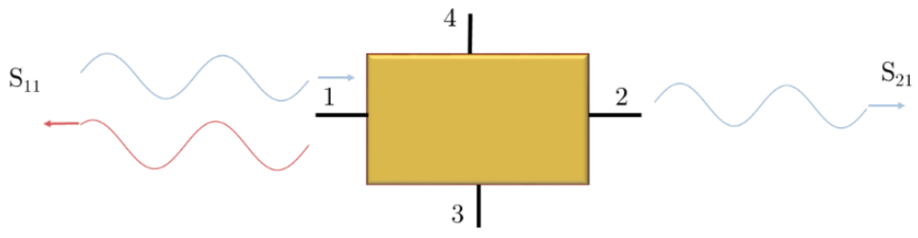
 [Green Version]
Figure 1. WR link model. The WR link model shows the hardware delays ( Δ ) of the master and slave clocks, as well as the delays in the fiber ( δ ).
Electronics 12 03394 g001
Figure 2. The architecture of the WR expansion board. The board is supplied at 5 V, from where all the needed voltages are generated.
Electronics 12 03394 g002
Figure 4. Phase noise plot for Abracon oscillators for an integration bandwidth from 12 kHz to 20 MHz.
Electronics 12 03394 g004
Figure 5. Schematic of the 125 MHz clock generator. It includes the two systems, the first system based on an oscillator of 125 MHz, and the second system in an oscillator of 25 MHZ and a CDCM61002 clock generator. An ADC is used to fine-tune the crystal with the WR control signal. The 124.992 generator has similar schematics.
Electronics 12 03394 g005
Figure 6. Layout of the PCB. A ground area has been defined for the oscillator system in order to reduce the noise in this critical system. The components are placed only on the top layer. Controlled impedance has been used to route critical tracks. The dimensions of the board are 88 mm × 50 mm.
Electronics 12 03394 g006
Figure 7. PCB Stackup. A width of 35 µm has been selected for the external layers, while 17 µm are used for the internal ones. The width of the dielectric is set to 225 µm, with a core of 1 mm.
Electronics 12 03394 g007
Figure 8. Geometry simulation for the external tracks to maintain a 100 Ω differential impedance. For the internal tracks, a 0.3 mm track separation was chosen and was swept with a track width from 0.2 mm to 0.24 mm. A track width of 0.27 mm for the external tracks was selected. Simulations were performed with ADS.
Electronics 12 03394 g008
Figure 9. Model in π equivalent of a via where the capacitances and parasitic inductance generated by its structure.
Electronics 12 03394 g009
Figure 10. Left: Model created for vias and antipads. Right: Antipad simulation to maintain a 100 Ω differential impedance.
Electronics 12 03394 g010
Figure 11. Impedance of the DDMTD PDN. The values of the decoupling capacitors have been optimized in ADS to reduce the PDN impedance as it is a source of SSN.
Electronics 12 03394 g011
Figure 12. Representation and nomenclature of a two-port network for the definition of the so-called S parameters.
Electronics 12 03394 g012
Figure 13. Relationship between the input and output waves that define the S 11 and S 21 parameters of a two-port network.
Electronics 12 03394 g013
Figure 14. Simulation of insertion and return losses (parameters SDD21 and SDD11) corresponding to the 125 MHz and 124.992 MHz clock lines. The differences between the two clock lines are due to the different track layouts.
Electronics 12 03394 g014
Figure 15. Simulation of FEXT crosstalk noise, both in differential and common mode, between two differential pairs corresponding to adjacent signals.
Electronics 12 03394 g015
Figure 16. Induced noise NEXT, in both differential and common mode, between two differential pairs corresponding to adjacent clock signals.
Electronics 12 03394 g016
Figure 17. Simulation of the characteristic impedances of the differential pairs with the longest length for the clock signals. The large negative discontinuities observed in this graph correspond to the capacitive effects produced at the end of the lines by the connection points of the connectors.
Electronics 12 03394 g017
Figure 18. Eye diagrams results for the clock lines of 125 MHz and 124.992 MHz. Both diagrams are open more than 80%.
Electronics 12 03394 g018
Table 1. Mixed S-parameter matrix for differential ports.
Differential SignalCommon Signal
Port 1Port 2Port 1Port 2
Differential SignalPort 1SDD 11 SDD 12 SDC 11 SDC 12
Port 2SDD 21 SDD 22 SDC 21 SDC 22
Common SignalPort 1SCD 11 SCD 12 SCC 11 SCC 12
Port 2SCD 21 SCD 22 SCC 21 SCC 22
Table 2. Measurement of the fluctuations produced in the clock lines.
ContributionAbracom
125 MHz124.992 MHz
Random Jitter RMS0.11 ps0.12 ps
Inter Symbols (ISI)0.09 ps0.14 ps
Duty Cycle distortion (DCD)0.01 ps0.01 ps
Periodic (PJ) RMS0.26 ps0.16 ps
Total1.56 ps1.74 ps
Eye aperture (width)94.6%95.3%
Eye aperture (height)97.1%83.4%
Disclaimer/Publisher’s Note: The statements, opinions and data contained in all publications are solely those of the individual author(s) and contributor(s) and not of MDPI and/or the editor(s). MDPI and/or the editor(s) disclaim responsibility for any injury to people or property resulting from any ideas, methods, instructions or products referred to in the content.

