Abstract
Stand-alone microgrids have become reliable and efficient solutions for remote areas and critical infrastructures. However, the converters within these microgrids experience long-term complex power fluctuations caused by random variations in micro sources and loads. These power fluctuations induce thermal cycling in semiconductor chips, leading to thermal fatigue failure and compromising the safety and reliability of both the converter and microgrid operation. To address this issue, this paper proposes a reactive power injection algorithm aimed at reducing the output power fluctuation of the converter. The algorithm implements reactive power injection at the converter control level, thereby restructuring the output power profile and resulting in reduced junction temperature fluctuations in IGBTs. This approach effectively mitigates thermal stress within the material layers of the module, extending the lifetime of power devices and improving the operational reliability of the microgrid. The algorithm implementation is based on the PQ control strategy, integrating the power triangle with the envelope detection technique. Furthermore, the lifetime prediction process utilizes the electro-thermal coupling model, the rainflow counting algorithm, and the Lesit model. Simulation results demonstrate that, for an active power fluctuation range of 10 kW to 80 kW and an equivalent RC time constant of 22.5 s, the algorithm achieves a significant reduction of 62.64% in the amplitude of output power fluctuation and extends the lifetime of power devices by 74.13%. The obtained data showcase the effectiveness of the algorithm in enhancing the lifetime of power devices and further improving the microgrid operational reliability under specific parameter conditions.
1. Introduction
Stand-alone microgrids are pivotal in integrating distributed power supply systems to provide electricity to regions lacking grid coverage. These microgrid systems have been widely adopted in various applications, including remote islands, border guard posts, and field camps [1,2,3]. Power electronic converters, as essential equipment in the microgrid, are responsible for producing, transforming, and utilizing the electrical energy within the system. However, these critical converters are exposed to complex power fluctuations due to intermittent distributed generation and random load shifting. Research has indicated that thermal cycling caused by power fluctuations can lead to thermal stress fatigue between different material layers within power semiconductor devices [4,5,6,7]. Prolonged accumulation of thermal stress fatigue can result in device failure, ultimately leading to converter breakdown. Figure 1 illustrates the significance of PV inverters and energy storage converters in generating and regulating electrical energy in stand-alone microgrids. Relevant data suggested that semiconductor failures are responsible for 50–80% of PV converter failures [8,9,10]. Similarly, such failures are expected to occur at a rate of 20–50% in energy storage converters [11,12]. The failure of these key converters significantly impacts the operational reliability of stand-alone microgrids, potentially leading to systemic outages and substantial economic losses.
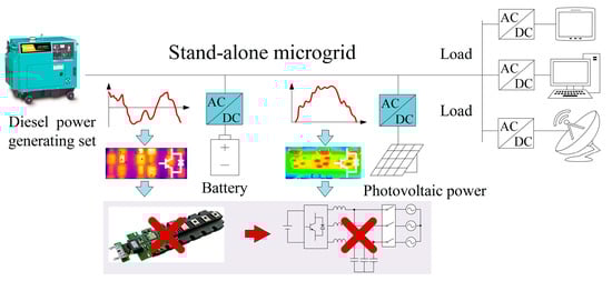
Figure 1.
Failure of critical converters due to complex power fluctuation.
Hence, it is imperative to address the critical issues of mitigating thermal stress fluctuations of power semiconductor devices and improving the operational reliability of the microgrid. Extensive research has been carried out by scholars in this field, which can be categorized into three main aspects:
(1) Device-level reliability management
Device-level reliability management aims to reduce thermal damage by modifying the switching frequency, modulation mode, or driving waveform of power devices. One approach proposed in [13] was to control the switching frequency to suppress the thermal stress fluctuation in IGBTs. Another method described in [14] reduced the junction temperature’s mean and amplitude values by limiting the current and switching frequency. In [15], a DSVPWM method was introduced to enhance the thermal reliability of a three-level inverter by adjusting the switching modes based on the load power factor. Similarly, the author in [16] proposed an algorithm to change the modulation strategy from DPWM to CPWM based on the probability distribution of wind speed. In [17], the driving voltage of IGBTs was adjusted in a closed loop to mitigate junction temperature ripple. Additionally, in [18], the turning off track of IGBTs was regulated to stabilize junction temperature fluctuations. These methods primarily focus on controlling power devices and involve adjustments in the control loop, drive circuit, and EMI suppression, among others. However, these approaches carry potential uncontrollable risks and may significantly deteriorate the converter’s output. Furthermore, their implementation processes are complex, making them challenging to apply in practical scenarios.
(2) Converter-level reliability management
Converter-level reliability management primarily focuses on multi-port converters, such as solid-state transformers. This approach involves evaluating the thermal stress risk or life cycle of each port and redistributing power from high-risk ports to low-risk ports. In the context of multi-port power electronic transformers, an algorithm was proposed in [19] to enhance the thermal reliability of the overall converter and extend the lifespan of critical power equipment by transferring the load from aging ports to healthy ports. Another study [20] evaluated the service life of each port in a four-port active full bridge converter and adjusted the droop coefficient to prolong the converter’s lifetime. These power control methods aim to redistribute and rebalance power within the converter but are limited to multi-port converters. Despite these efforts, the converter’s output power fluctuations have not undergone significant changes, and as a result, the deep cycling of junction temperature in power devices persists.
(3) System-level reliability management
System-level reliability management primarily relies on the implementation of the Power Network Reconfiguration (PNR) method. This approach entails utilizing algorithms to reconfigure the power network, with the goal of reducing the frequency and duration of system outages and enhancing the overall reliability of the system. In [21] and [22], a new optimization technique of the jellyfish search (JFS) algorithm and a novel optimization approach based on the Social Network Search (SNS) algorithm were, respectively, employed for distribution network reconfiguration aimed at improving reliability. In [23], a modified jellyfish search (MJFS) algorithm was presented to address optimal network reconfiguration (ONR) in medium voltage distribution feeders. Additionally, in [24], a microgrid (MG) operating strategy based on the developed equilibrium optimization (EO) was adopted to minimize the operational costs and emissions while greatly reducing the active power losses. Typically, the aforementioned methods are effective in enhancing the microgrid operational reliability at the system level. However, the efficacy of these methods becomes constrained when converters associated with multiple micro sources experience complex power fluctuations caused by load variations or other factors.
In addition to the previous studies, further research has indicated that the injection of reactive power has an impact on the junction temperature of power devices. Notably, the literature [25] includes relevant findings from Professor Frede Blaabjerg’s team at Aalborg University, Denmark. The research primarily focused on the grid-side converter of the doubly fed wind turbine. It started with the assumption that reactive power has the potential to alter the angle of the grid-side input current. Through the analysis of current and thermal load data at various wind speeds, the researchers concluded that the inclusion of inductive reactive power resulted in increased power loss in the grid-side converters. This finding has implications for the junction temperature control of power devices. In [26], the author proposed a junction temperature closed-loop control system to regulate the allocation of reactive power, effectively reducing the fluctuation of junction temperature in IGBTs. Consequently, the aforementioned research yielded preliminary findings indicating that reactive power has an impact on the junction temperature of power devices in specific solutions. However, the evidence presented in the research did not establish a direct correlation between reactive power injection and the lifetime of power devices.
Building upon the insights gained from the analysis above, this paper presents a reactive power injection algorithm at the control level of the converter to improve the microgrid operational reliability. The primary objective of this method is to mitigate the output power fluctuations of the converter, leading to an extension in the lifetime of power devices. The overall output power curve of the converter can be restructured by employing the PQ control strategy, integrated with the envelope detection technique and the reactive power injection algorithm. In addition, the lifetime prediction process involves the electro-thermal coupling model, the rainflow counting algorithm and the Lesit model. The main contributions of this paper are as follows:
- (1)
- This paper presents a reliability enhancement strategy that utilizes apparent power reconstruction to optimize the shape of the power curve and make efficient use of the converter’s remaining capacity. By reducing power fluctuations and mitigating junction temperature fluctuations in power devices, the proposed method extends their lifetime and improves the operational reliability of the microgrid. The strategy achieves power curve reconstruction by controlling reactive power injection within the PQ loop, offering the advantages of easy integration and simple control.
- (2)
- In this paper, we propose a reactive power injection algorithm for mitigating power fluctuations. The algorithm involves establishing the extraction of the enveloped power curve and calculating the amount of reactive power injection in real-time based on the power triangle.
The paper is organized as follows: Section 2 provides an overview of the algorithm and the verification process. Section 3 presents the envelope detection and reactive power injection algorithm. In Section 4, the methodology for evaluating the reliability of IGBT modules is described, including the estimation of junction temperature using the electro-thermal coupling model and the evaluation of module lifetime using the rainflow counting method with the Lesit model. Section 5 presents the simulation results, and Section 6 concludes the paper with a discussion.
2. Overview of Algorithm and Verification
2.1. PQ Control Strategy
The PQ control strategy is a widely adopted control method in microgrid systems. Figure 2 illustrates the PQ control loop implemented in a three-phase grid-connected inverter. The control loop consists of an outer-power loop and an inner-current loop. This strategy regulates the output active and reactive power of the micro source, thereby ensuring the stable operation of the grid-connected system [27].
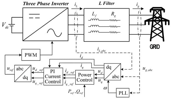
Figure 2.
PQ control loop in grid-connected inverter.
The implementation process of the PQ control strategy is shown in Figure 2. Initially, the grid-side voltage (ug,abc) and inductive current (iL,abc) serve as inputs to the phase-locked loop (PLL) and coordinate transformation, resulting in the generation of current (id, iq) and voltage (ud, uq) in the d-q axis. Subsequently, the power reference signal (Pref, Qref) and voltage (ud, uq) are fed into the power loop, leading to the calculation of current reference signals (I_dref, I_qref). Then, the voltage reference signals (u_dref, u_qref) in the d-q axis are then determined by comparing the current reference signals (I_dref, I_qref) with the current values (id, iq) in the inner-current loop. Finally, the switching signal for the power devices is obtained through the inner-current loop, coordinate transformation, and pulse width modulation (PWM) module. This allows for precise control of the power delivered by the inverter to track the desired reference value [28]. The proposed algorithm in this paper is based on the PQ control strategy, primarily utilized to simulate complex power fluctuations resulting from random variations in micro sources and loads by modifying the power reference value.
2.2. The Restructuring Process of the Output Power Curve
This study aims to investigate the potential impact on the reliability of power devices by reducing the output power fluctuations of the converter. The proposed algorithm focuses on restructuring the output power curve of the converter through reactive power injection. The restructuring process primarily relies on the PQ control strategy, integrating the envelope detection with the reactive power injection algorithm. Figure 3a illustrates the process of restructuring the output power curve. Initially, the active power reference Pref is set as a fluctuating curve, while the reactive power reference Qref remains constant. The PQ control strategy is employed to accurately track the power reference signal, resulting in a fluctuating pattern of the converter’s output apparent power. As shown in Figure 3b, the red curve represents the task curve of the converter, which simulates the power fluctuations resulting from variations in micro-source and load. The envelope detection technique is then applied to obtain the enveloped curve, which serves as the target curve for the converter. However, the process of restructuring the output power curve involves another crucial step, namely reactive power injection. The amount of reactive power injection is determined by the reactive power injection algorithm, which compares the envelope curve with the task curve. Consequently, while the active power reference remains unchanged, the reactive power reference is adjusted by adding the injected reactive power amount to the original constant value. Subsequently, the PQ control strategy is employed to restructure the output power curve from the task curve to the target curve and effectively reduce the original power fluctuations. Nonetheless, the impact of the proposed algorithm on the reliability of power devices remains uncertain. Therefore, a reliability evaluation process is necessary to validate the effectiveness of the algorithm.
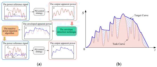
Figure 3.
The restructuring process of the output power curve. (a) Algorithm implementation flowchart, (b) The output power curve of the converter.
2.3. Reliability Evaluation of IGBT Modules
A cross-section view of the IGBT model is shown in Figure 4a, which highlights the various layers of materials used in its packaging. These layers include bond wires, silicon chips, solder layers, copper layers, a ceramic layer, and a base plate [29]. These materials have different coefficients of thermal expansion (CTE), leading to inconsistent thermal expansion behavior. Extensive research has been conducted on the thermal damage mechanism of power devices, revealing that prolonged thermal cycling results in varying thermal stresses among the material layers within the module due to their different CTEs. These thermal stresses contribute to wire-bond liftoff and solder joint fatigue, which are the primary causes of power device failure [30,31,32,33].
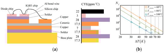
Figure 4.
The structure and the power cycling lifetime of the IGBT module. (a) The cross-section of an IGBT module, (b) The characteristic curve of power cycling lifetime in IGBT modules.
Figure 4b presents the characteristic curves depicting the influence of junction temperature swing (ΔT) and mean junction temperature (Tj_mean) on the power cycling lifetime of the IGBT module [5]. The data in the figure demonstrate a decrease in the power cycling lifetime as Tj_mean increases, and they show an exponential damping trend with the rise in ΔT. Therefore, in order to further assess the reliability of the IGBT module, it is essential to obtain junction temperature data.
As depicted in Figure 5, two major steps are comprised in the reliability evaluation of IGBT modules: the junction temperature estimation and the lifetime evaluation. Firstly, the RC parameters within the thermal model are derived by analyzing the transient thermal impedance curve provided in the IGBT datasheet, and the Foster equivalent thermal network is established. Moreover, the power loss can be determined by importing the load current Ic, the duty ratio and other relevant parameters from the converter operation into the power loss model. In this case, the electric and thermal models are coupled to obtain the junction temperature. Then, load cycles extracted by the rainflow counting algorithm from junction temperature are adopted in the life prediction model and then the miner accumulation theory. Finally, the accumulated fatigue damage, a critical parameter for assessing the reliability of the IGBT module, is determined.
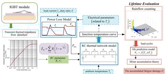
Figure 5.
The procedure for evaluating the reliability of the IGBT module.
3. Envelope Detection and Reactive Power Injection Algorithm
3.1. Principle of Apparent Power Envelope Detection
The envelope detector circuit is shown in Figure 6a. When the Vin(t) is positive, the diode D1 conducts, and the capacitor C is charged. In addition, the charging process will not interrupt until the capacitor voltage reaches the peak of the input voltage. Beyond the peak point, the diode is reverse-biased, and the capacitor is slowly discharged through the resistor RL. Its output voltage is depicted in Figure 6b by a solid curve, which approximately follows the signal envelope. The appropriate envelope extraction implies a proper choice for the time constant of the corresponding RC circuit, = RLC.
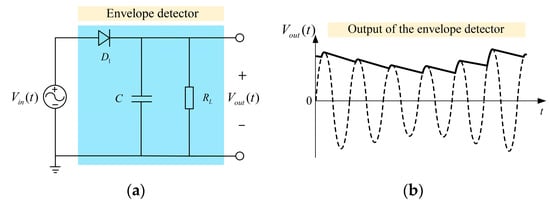
Figure 6.
Envelope detector. (a) Circuit, (b) Output of the envelope detector.
The approach of enveloping the apparent power is based on the envelope detector circuit. The basic principle is indicated in Figure 7a, which is importing the apparent power Sref into the controlled voltage source as the input signal. Through the operation of the diode and the RC network, the enveloped apparent power Sevp is obtained as the output of the circuit. Moreover, the extraction of the envelope will exhibit variations depending on the chosen parameters of the RC network.
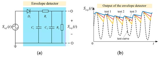
Figure 7.
Apparent power envelope detector. (a) Circuit, (b) Output of the envelope detector.
As shown in Figure 7b, the mathematical relationships between the corresponding parameters of the test curves and detection time should be given by:
where SAM(t) is the expression of the test curve, SCM is the carrier amplitude, ma is the amplitude modulation factor (0 < ma < 1), Ω is the angular frequency of the low-frequency signal, and ωc is the angular frequency of the high-frequency carrier. To avoid inertial distortion, the maximum of equivalent RC parameters needs to satisfy (2). When conducting engineering analysis, it is generally recommended that the value of is no more than 1.5. However, in order to further enhance the detection voltage transmission coefficient and high-frequency filtering capability, the value range of equivalent RC parameters should satisfy (3) [34]. In Figure 7b, as the RC time constant decreases, the discharge time of the circuit becomes shorter, resulting in a change in the shape of the envelope curve from “test 1” to “test 3”.
3.2. Principle of Reactive Power Injection Algorithm
The task curve (red curve) and the target curve (blue curve) of the converter are depicted in Figure 8a. The task curve represents the power fluctuations experienced by critical converters due to intermittent distributed generation and random load switching. The objective is to restructure the converter’s output power to closely match the target curve, which results in a significant reduction in power fluctuations. Achieving this requires modifying the reactive power reference signal within the PQ control strategy. The reactive power injection algorithm plays a crucial role in determining the amount of reactive power injection needed. This algorithm takes into account the enveloped curve (discussed earlier) and the task curve to calculate the appropriate amount of reactive power injection. In the following section, we will provide detailed explanations of the reactive power injection algorithm.
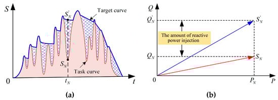
Figure 8.
The output power curve of the converter. (a) The output power curve, (b) The power triangle at tN.
Figure 8b illustrates the output power of the task curve at the moment tN, denoted as SN, and the output power of the target curve is denoted as S′N. Furthermore, the vector decomposition of SN derives the active power component PN and the reactive power component QN, and the vector decomposition of S′N yields the component of active power PN and reactive power Q′N. The amount of reactive power injection ∆Q is equal to the subtraction of QN from Q′N. Thus, based on the power triangle, the principle of reactive power injection is given by:
The amount of reactive power injection at tN can be derived by (6). However, the task curve exhibits a random fluctuation pattern over time. To restructure the task curve into the target curve, the magnitude of reactive power injection needs to vary accordingly. As depicted in Figure 9a,b, the output power of the task curve at moments t1, t2 and t3 is denoted as S1, S2 and S3, respectively. The active power components decomposed from S1, S2 and S3 correspond to P1, P2 and P3, respectively, while the reactive power components remain as QN, a constant value. Furthermore, the output power of the target curve at moments t1, t2 and t3 refers to S′1, S′2 and S′3, respectively. In addition, the amount of reactive power injection at these three moments is denoted as ΔQ1, ΔQ2 and ΔQ3, respectively.
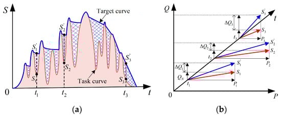
Figure 9.
The output power curve of the converter. (a) The output power curve, (b) The power triangle at t1, t2 and t3.
In this condition, the amount of reactive power injection varies continuously with time, which can be derived by:
The reactive power reference of the target curve Qref(t) is defined as:
By substituting (9) into (10), the following expression is obtained:
Equation (11) represents the reactive power reference signal, which is determined by importing the enveloped curve and the task curve into this equation, characterized by injecting a fluctuation curve on the constant QN. When the active power reference is set as P(t), and the reactive power reference is set as Qref(t), the output power curve of the converter can be approximately restructured into the target curve through the PQ control strategy. Eventually, the restructuring process of the converter’s output power curve is accomplished. Nevertheless, the proposed algorithm’s impact on power device reliability remains uncertain. Therefore, conducting a reliability evaluation process for power semiconductor devices is necessary.
4. Reliability Evaluation of IGBT Modules
4.1. Analysis of Electro-Thermal Coupling Model
To assess the reliability of IGBT modules, the initial step involves estimating the junction temperature. In this regard, the electro-thermal coupling model is widely utilized as an analytical model. The electro-thermal coupling model, depicted in Figure 10, consists of two main components: the power loss calculation and the thermal network model. This model captures the interconnected nature between electrical and thermal properties in power devices, indicating a dynamic interaction effect between electric parameters and junction temperature.
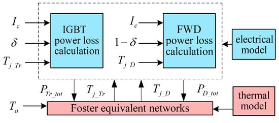
Figure 10.
Electro-thermal coupling model.
In the implementation process, the initial step involves incorporating the operational parameters of power devices into the electrical model to calculate the power loss. Subsequently, the obtained power loss is utilized in the thermal model to estimate the junction temperature, which is then fed back into the electrical model for parameter adjustment until a stable junction temperature is achieved. The duty ratio for IGBTs is denoted as , and the duty ratio for FWD is denoted as . Moreover, Tj_Tr and Tj_D refer to the junction temperature of IGBTs and FWD, respectively, and the current is denoted as Ic. In most cases, the off-state loss of IGBT and FWD is considered a small portion of the total loss. Therefore, as the power loss of IGBT, PTr_tot is composed of switching and conduction losses. Similarly, as the power loss of FWD, PD_tot contains conduction and reverses recovery losses [35].
4.1.1. Power Loss
In Figure 11, as the IGBT module is turned on, the current ic flowing through the chip rises sharply, and the voltage Vce drops to saturation rapidly. Because of the internal resistance of the chip, the saturation voltage drop is not zero. When the current ic and the saturation voltage drop exist simultaneously, conduction losses occur.
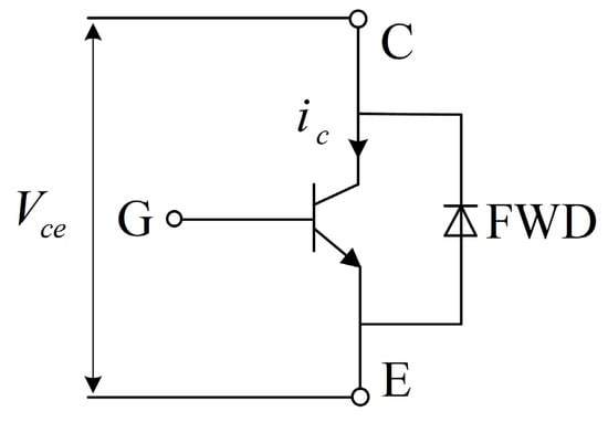
Figure 11.
IGBT module.
During the carrier period, Tsw, ic flows through IGBT within , and current flows through the diode during the remaining time . In most cases, the load current can be taken as a constant during the switching cycle Tsw. Thus, the conduction energy of the IGBT in a switching cycle has the form:
The average power loss in a switching cycle can be further defined as:
Similarly, the average power loss of the diode in the switching cycle can be written in the form:
For IGBTs with FWD, the conduction voltage drop varies as the temperature changes, which can be approximated as:
where Vce and VF denote the actual conduction voltage drop of IGBT and FWD, respectively. rce_25°C and rF_25°C refer to the rated on-state resistance of IGBT and FWD at 25 °C, respectively. Vce_25°C and VF_25°C correspond to the rated on-voltage drop of IGBT and FWD at 25 °C [36]. The actual junction temperature of IGBT and FWD is denoted as Tj_Tr and Tj_D, respectively. Kr_Tr, Kr_D, KV_Tr, and KV_D represent the temperature coefficients of the influence of temperature on the on-resistance and on-voltage drop of IGBT and FWD [37]. These coefficients can be determined using the following equations:
In most cases, the IGBT and FWD’s on-resistance and on-voltage demonstrate temperature-dependent variations relative to the junction temperature. Generally, the datasheet of the IGBT includes characteristic curves that depict the device’s behavior at different junction temperatures, such as 25 °C, 125 °C, and 150 °C. In (17) and (18), IGBT and FWD’s rated on-state voltage drop and rated on-state resistance in characteristic curves are selected for linear interpolation. Substituting (15) and (16) into (13) and (14), respectively, the conduction power losses of the IGBT and FWD can be expressed as:
where the conduction power of the IGBT is denoted as Pcond_Tr, and the conduction power of the FWD is denoted as Pcond_D [38]. Eventually, the conduction power losses of the IGBT and FWD can be derived by (19) and (20).
4.1.2. Switching Loss
As the IGBT’s switching frequency increases, the proportion of switching losses in the overall device loss progressively escalates, and the switching losses demonstrate variations in accordance with fluctuations in the junction temperature and external conditions. Typically, the quadratic curve fitting method is predominantly employed for calculating the switching loss, utilizing the characteristic curve of switching losses with current at rated parameters as presented in the datasheet. Moreover, it is essential to consider the difference between the actual and the reference voltages. The switching losses of IGBT and FWD can be represented as:
where fs represents the carrier frequency, Eon, Eoff, and Err represent the turn-on loss, turn-off loss of IGBT, and reverse recovery loss of FWD, respectively. These parameters can be obtained from the loss curve provided in the datasheet. Vcc denotes the bridge arm voltage, while Irated and Vrated correspond to the reference current and the reference voltage, respectively. KswTr_I and KswD_I represent the current coefficient that influences the switching losses of the IGBT module with respect to current amplitude [39]. Similarly, KswTr_V and KswD_V represent the voltage coefficient that affects the switching losses of the IGBT module in relation to the bridge arm voltage. Lastly, KswTr and KswD denote the temperature coefficient that influences the switching losses of the IGBT module due to temperature changes. In general, the empirical values of KswTr and KswD are commonly set to 0.03 and 0.06, respectively [40].
4.1.3. Thermal Model
The thermal characteristics of the device in the equivalent thermal network model are commonly represented using the RC circuit. Two commonly used models for expressing these characteristics are the Cauer and the Foster thermal model. However, the Foster thermal model is preferred in application due to its easily obtainable parameters. As is shown in Figure 12, the Foster thermal networks are characterized by the equivalent one-dimensional heat conduction model [41]. According to the analogy theory of heat and electricity in the model, the voltage corresponds to the junction temperature, while the power loss corresponds to the current. The resistance and capacitance in the model represent thermal resistance and thermal capacitance, respectively [42].
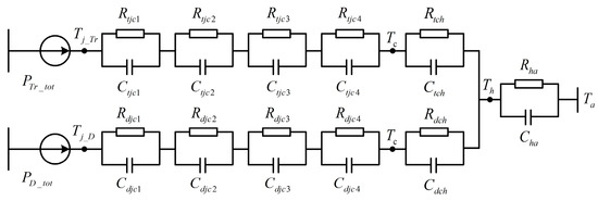
Figure 12.
Foster thermal networks.
where PTr_tot/PD_tot represents the average loss of IGBT/FWD in the switching cycle, Tj_Tr/Tj_D denotes the junction temperature of the IGBT/FWD, and Rtjc1-4/Rdjc1-4 represents the thermal resistance of the IGBT/FWD from the junction to the case. Additionally, Ctjc1-4/Cdjc1-4 represents the thermal capacitance of the IGBT/FWD from the junction to the case, Tc signifies the case temperature, Rtch/Rdch corresponds to the thermal resistance of the IGBT/FWD from the case to the heat sink, and Ctch/Cdch represents the thermal capacitance of the IGBT/FWD from the case to the heat sink. Furthermore, Th denotes the heat sink temperature, Rha represents the thermal resistance from the heat sink to the ambient, Cha signifies the thermal capacitance from the heat sink to the ambient, and Ta denotes the ambient temperature [43].
The transient thermal impedance curve has the form:
The parameters of Foster thermal networks can be obtained by fitting the transient thermal impedance curve of the device using the fitting toolbox based on MATLAB [44]. Generally, the fourth-order thermal network parameters are given in the datasheet. In addition, the power semiconductor device selected in this paper is Infineon FF300R17ME4. Table 1 shows the parameters of the Foster model. Moreover, the time constant is the product of thermal resistance and thermal capacitance, and the ambient temperature Ta is set as 40 °C.

Table 1.
The parameters of the Foster model.
4.2. Analysis of Lifetime Evaluation of the IGBT Module
To achieve the reliability evaluation of IGBT modules, this section conducts a lifetime evaluation based on the profile of the junction temperature. The following steps comprise this procedure: Firstly, the rainflow counting method is employed to extract the thermal cycle distribution of the junction temperature swing ΔT and mean junction temperature Tj_mean, which are the essential data for the lifetime evaluation. Subsequently, the number of cycles to failure corresponding to different thermal cycles can be derived by importing the relevant data into the Lesit model. Eventually, based on Miner’s rule, the damage degree related to different thermal cycles is added to obtain the accumulated fatigue damage of the IGBT module, thereby accomplishing the reliability evaluation process.
4.2.1. Rainflow Counting Method
During the operation of power semiconductor devices, the thermal cycles within the chips varied according to the mission profile variation. The long-term accumulated fatigue damage caused by various thermal stress leads to the failure of power devices. Here, a method is employed to accurately calculate the number of cycles for each combination of mean and range, aiming to reveal the effect of thermal cycling, which is known as rainflow cycle counting [45]. As depicted in Figure 13, the rainflow counting method statistically translates the complex thermal stress profile into the regular thermal cycle.
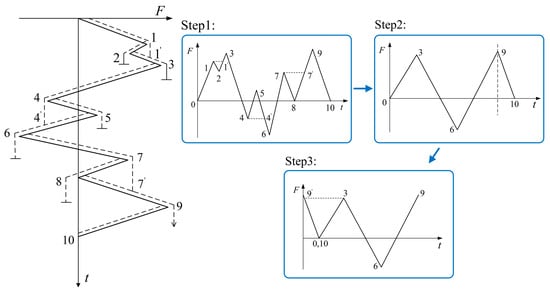
Figure 13.
The rainflow counting method.
The load-time process curve data are rotated by 90°, with the vertical coordinate representing time and the horizontal coordinate representing load. The trace connecting point 1 to point 10 forms the original load curve. And the method involves tracing the rain flow along each layer, starting from the peak and valley values indicated by the dotted line in Figure 13. In this paper, the junction temperature profile is analyzed using this method to count the number of cycles (ni), the junction temperature swing (ΔT), and the mean junction temperature (Tj_m). Each temperature cycle is characterized by three points and can be categorized as minor or major cycles based on the swing and average value. In the first step, minor cycles (1-2-1′, 4-5-4′, and 7-8-7′) are extracted, and the corresponding ΔT and Tj_m are recorded. The points composing the minor cycles are then removed. Subsequently, the waveform is restructured in steps 2 and 3 to identify and save the ΔT and Tj_m values for major cycles (9′-0-3, 3-6-9). Finally, these data are used in the life prediction model to evaluate the reliability of power devices [46,47].
4.2.2. Lesit Model
The Lesit model, developed by a research team in Switzerland, is widely utilized as a significant life prediction model in various industrial applications. Based on power cycle experiments, it has been observed that device failure is primarily associated with the average junction temperature and its fluctuation amplitude. In contrast to the Coffin–Manson model, the Lesit model considers the impact of both the junction temperature swing ΔT and the mean junction temperature Tj_m on the lifetime of the power device [48]. Consequently, this formula effectively captures the failure mechanism of power devices. The mathematical expression of the Lesit model is as follows:
where Nf denotes the numbers to failure corresponding to specific temperature cycles (ΔT, Tj_m), A represents a parameter related to the characteristic of the power device, a is a fitted value from the data of the IGBT lifetime module, and Ea represents the activation energy related to the material. In this paper, we chose A = 1300, a = −6.14, Ea = 7.8 × 10⁴ J/Mol, and K = 8.314 J/mol.K [49].
Miner’s rule is a commonly used cumulative damage theory for failures caused by fatigue [50]. It is employed to evaluate the accumulated fatigue damage of the IGBT module here. Based on the Miner linear accumulation damage theory, when the material is subjected to the stress waveform constructed with m types of stress components, the accumulated fatigue damage is given by:
where ni is the cycle number of the stress component Si that can be obtained from the rainflow algorithm. Each stress component corresponds to a temperature cycle characterized by specific ΔT and Tj_m. The cycle times Ni can be derived by Lesit model. Moreover, when the variable stress spectrum is executed for T times(lifetime), the failure occurs by fatigue, we therefore write [51]:
The criterion of failure by fatigue can be written as follows [52]:
5. Simulation Results and Analysis
In this section, the reactive power injection algorithm is employed in the converter’s output power curve restructuring, and its impact on the reliability of the IGBT modules is discussed. The verification process focuses on two key variables: the task curve and the equivalent RC time constant. These variables are utilized to adjust the power fluctuation and the depth of the envelope, respectively. In the first scenario, the task curve is modified by varying the active power reference, resulting in different fluctuation profiles of the converter’s output power. Furthermore, it is important to note that the equivalent RC time constant remains constant throughout the process, allowing for an investigation into the effectiveness of the reactive power injection algorithm under varying power fluctuation conditions. In the second scenario, the envelope depth is adjusted by modifying the equivalent RC parameters, leading to various target curves for the converter’s output power curve. The fluctuation pattern of the task curve is kept constant, and the investigation primarily focuses on examining the impact of the reactive power injection amount on the reliability of the IGBT module.
The algorithm is implemented and verified on the Matlab platform in this paper, and the reliability evaluation procedure of the IGBT module is illustrated in Section 2. Simulation parameters are listed in Table 2.
Table 2.
Simulation parameters.
5.1. Scenario 1
In this scenario, the junction temperature and lifetime of the IGBT module are related to the task curve’s variation. The reactive power reference is set at 20 kVA, and the output task curve can be modified by adjusting the active power reference Pref. Throughout the process, the equivalent RC time constant remains 22.5 s. Figure 14a,c represent the output power curve corresponding to Pref ranging from 10 kW to 80 kW and 50 kW to 80 kW, respectively. Sampling from 1.0 s in Figure 14a, the task curve has a maximum output power of 79.10 kW and a minimum output power of 18.39 kW. Moreover, the target curve exhibits a maximum output power of 85.93 kW and a minimum output power of 63.25 kW, which indicates that the algorithm effectively reduces the amplitude of output power fluctuation by 62.64%. In Figure 14c, the task curve and target curve display a power fluctuation of 28.23 kW and 13.35 kW, respectively. In this case, the algorithm reduces the amplitude of output power fluctuation by 52.71%. Additionally, Figure 14b and Figure 14d depict the junction temperature profiles corresponding to Figure 14a and Figure 14c, respectively. Taking a sample from 1.0 s in Figure 14b, the junction temperature before reactive power injection reaches a maximum of 74.36 °C and a minimum of 59.18 °C, and the ΔT is 15.18 °C. The ΔT of junction temperature after reactive power injection refers to 7.45 °C. It demonstrates that the algorithm reduces the fluctuation of junction temperature by 50.92%. Similarly, in Figure 14d, the junction temperature before and after reactive power injection has a ΔT of 8.96 °C and 4.77 °C, respectively. In addition, a reduction of 46.76% in the fluctuation of junction temperature is achieved by the algorithm.
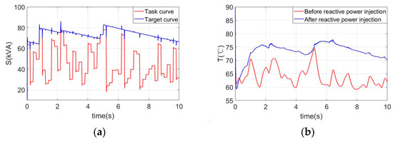
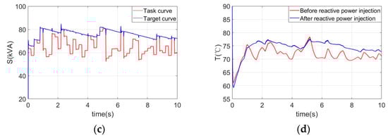
Figure 14.
The output power curve of the converter and the junction temperature curve. (a) The output power curve (Pref = 10 kW~80 kW), (b) The junction temperature of the IGBT module (Pref = 10 kW~80 kW), (c) The output power curve (Pref = 50 kW~80 kW), (d) The junction temperature of the IGBT module (Pref = 50 kW~80 kW).
The distribution of cycles associated with Tj_mean and ΔT can be derived by substituting the junction temperature data into the rainflow counting method, with the sampling rules described in Table 2. The rainflow counting results shown in Figure 15a,b correspond to the junction temperature before and after reactive power injection depicted in Figure 14b. In Figure 15a, the distribution of Tj_mean for cycles ranges between 60 °C and 67 °C, encompassing a total of 10 cycles, and the ΔT of cycles ranges from 0 °C to 4 °C. Whereas the Tj_mean of cycles in Figure 15b is distributed between 73 °C and 80 °C, with a total of 24 cycles, the ΔT of most cycles is below 1 °C. Figure 15c indicates the rainflow counting result of the red curve in Figure 14d. The Tj_mean of 13 cycles is distributed between 70 °C and 74 °C, and the ΔT ranges from 0 °C to 4 °C. By contrast, the rainflow counting result of the blue curve in Figure 14d is shown in Figure 15d. The distribution of Tj_mean for 16 cycles ranges between 75 °C and 79 °C, with the majority being minor cycles characterized by ΔT values below 2 °C. With the implementation of the algorithm, it can be observed that the mean value of the junction temperature cycle increases while the amplitude of the cycle decreases. Consequently, this process leads to an increase in the number of minor cycles.
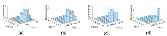
Figure 15.
The rainflow counting results. (a) The rainflow counting result of the red curve in Figure 14b, (b) The rainflow counting result of the blue curve in Figure 14b, (c) The rainflow counting result of the red curve in Figure 14d, (d) The rainflow counting result of the blue curve in Figure 14d.
Substituting the relevant data into the Lesit model and integrating them with Miner’s rule, the accumulated fatigue damage of the IGBT module for Figure 15a, Figure 15b, Figure 15c, and Figure 15d refers to 2.1604 × 10⁻¹⁰, 5.5886 × 10⁻¹¹, 3.9386 × 10⁻¹¹, and 3.4084 × 10⁻¹¹, respectively. Hence, considering the parameter settings outlined in this scenario, when the active power reference ranges from 10 kW to 80 kW and 50 kW to 80 kW, the algorithm effectively mitigates the damage degree of the IGBT module by 74.13% and 13.46%, correspondingly. In accordance with Equation (27), the lifetime of the IGBT module can be extended by 74.13% and 13.46%, thereby improving the module’s reliability. In order to obtain general conclusions, four sets of comparison data were added to the original ones by changing the reference value of active power while ensuring that the equivalent RC parameters remain unchanged. As illustrated in Table 3, under the conditions of the active power reference within the ranges of 20 kW to 80 kW, 30 kW to 80 kW, 40 kW to 80 kW, and 60 kW to 80 kW, the algorithm effectively extends the lifetime of the IGBT module by 69.59%, 51.77%, 39.66%, and −8.34%, respectively.
Table 3.
Simulation data in different active power reference conditions.
Figure 16 visually presents the impact of the reactive power injection algorithm on the reliability of power devices under varying power fluctuation conditions. The data from Table 3 are represented in the form of a bar chart. The algorithm demonstrates its effectiveness in improving reliability when significant power fluctuations are present. However, as the power fluctuation decreases and becomes minor, the algorithm’s ability to enhance reliability diminishes. Notably, in the sixth data set, the algorithm may even lead to reduced reliability.
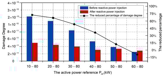
Figure 16.
Accumulated fatigue damage under various power fluctuations for the IGBT module.
The reactive power injection algorithm effectively reduces junction temperature fluctuations, thereby enhancing the reliability of power devices. However, it is important to note that the algorithm simultaneously increases the average junction temperature. Therefore, a careful assessment of the power fluctuation level and system characteristics is necessary before implementing the algorithm to ensure that it effectively enhances device reliability without compromising overall performance.
In addition to power fluctuation, the amount of reactive power injection is a crucial parameter in the implementation of the algorithm. Hence, it is essential to investigate the impact of the injection amount on the reliability of the IGBT module, which will be discussed in detail in the subsequent scenario.
5.2. Scenario 2
In this scenario, the junction temperature and lifetime of the IGBT module are related to the equivalent RC time constant . The specific implementation involves modifying the equivalent RC parameters while keeping the test curve unchanged. In addition, the amount of reactive power injection is adjusted by varying the equivalent RC parameters. The process ensures that the active power ranges from 40 kW to 80 kW while the reactive power remains fixed at 20 kVA. The adopted of Figure 17a and Figure 17c correspond to 5 s and 40 s, respectively. In Figure 17a, the task curve displays a maximum output power of 79.88 kW and a minimum output power of 42.57 kW. Moreover, the target curve has a fluctuation value of 24.64 kW. This reveals that the algorithm reduces the output power fluctuation by 33.96%. In Figure 17c, the task curve and target curve depict a power fluctuation of 37.31 kW and 15.14 kW, respectively. In this case, the algorithm reduces the fluctuation by 59.42%. Furthermore, Figure 17b and Figure 17d illustrate the junction temperature profiles corresponding to Figure 17a and Figure 17c, respectively. In Figure 17b, the junction temperature before reactive power injection reaches a maximum of 77.41 °C and a minimum of 66.41 °C. In addition, the ΔT of junction temperature after injection refers to 9.76 °C. It reveals that the algorithm reduces the fluctuation of junction temperature by 11.27%. Similarly, in Figure 17d, the junction temperature before and after reactive power injection has a ΔT of 11 °C and 4.83 °C, respectively. In addition, the algorithm successfully achieves a reduction of 56.09% in the fluctuation of the junction temperature.
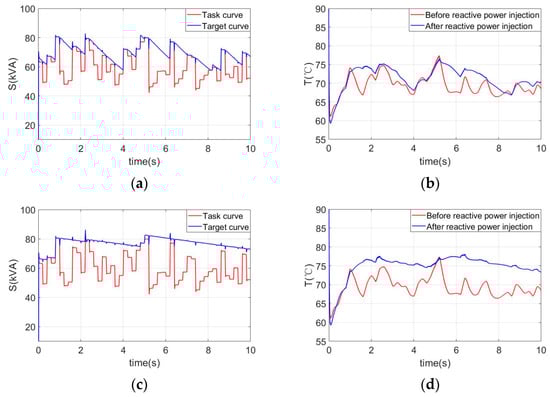
Figure 17.
The output power curve of the converter and the junction temperature curve. (a) The output power curve ( = 5 s), (b) the junction temperature of the IGBT module ( = 5 s), (c) the output power curve when ( = 40 s), (d) the junction temperature of the IGBT module ( = 40 s).
The rainflow counting results depicted in Figure 18a,b correspond to the junction temperature before and after reactive power injection as shown in Figure 17b. In Figure 18a, the distribution of Tj_mean for cycles ranges from 67 °C to 72 °C, encompassing a total of 13 cycles, and the ΔT of cycles ranges from 0 °C to 4 °C. Similarly, in Figure 18b, the Tj_mean of cycles is distributed between 69 °C and 77 °C, with a total of 15 cycles, and the ΔT of most cycles are below 2 °C. Furthermore, Figure 18c illustrates the rainflow counting result of the red curve in Figure 17d, where the Tj_mean of 13 cycles is distributed between 67 °C and 72 °C, and the ΔT ranges from 0 °C to 4 °C. In contrast, Figure 18d showcases the rainflow counting result of the blue curve in Figure 17d, where the distribution of Tj_mean for 24 cycles ranges from 75 °C to 80 °C, with the majority representing minor cycles characterized by ΔT values below 1 °C. As a result of the reactive power injection algorithm, the number of minor cycles increases. This indicates that the algorithm effectively reduces the amplitude of the junction temperature cycle and leads to a higher occurrence of minor cycles. By reducing the cycle amplitude, the algorithm helps mitigate the thermal stress on the power devices, which contributes to improving the reliability and lifetime of the power devices.
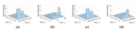
Figure 18.
The rainflow counting results. (a) The rainflow counting result of the red curve in Figure 17b, (b) The rainflow counting result of the blue curve in Figure 17b, (c) The rainflow counting result of the red curve in Figure 17d, (d) The rainflow counting result of the blue curve in Figure 17d.
By substituting the relevant data into the Lesit model and applying Miner’s rule, the accumulated fatigue damage for Figure 18a, Figure 18b, Figure 18c, and Figure 18d is calculated as 5.4057 × 10⁻¹¹, 3.3294 × 10⁻¹¹, 5.4057 × 10⁻¹¹, and 5.0462 × 10⁻¹¹, respectively. Thus, considering the parameter settings delineated in this scenario when the equivalent RC time constant is defined as 5 and 40, the algorithm effectively prolongs the lifetime of the IGBT module by 38.41% and 6.65%, respectively. Another four sets of contrast items were added to the original ones by changing the equivalent RC parameters. As indicated in Table 4, when the equivalent RC time constant is set to 15 s, 20 s, 30 s, and 50 s, the algorithm demonstrates the ability to extend the lifetime of the IGBT module by 43.03%%, 41.97%, 21.50%, and -3.88%, respectively.
Table 4.
Simulation data in different equivalent RC parameters conditions.
As depicted in Figure 19, the first to third sets of data demonstrate the effectiveness of the algorithm in improving power device reliability. Within a given power fluctuation condition, there exists an optimal amount of reactive power injection that maximizes the algorithm’s effectiveness in enhancing reliability. This optimal injection amount strikes a balance between reducing power fluctuations and minimizing the increase in average junction temperature.
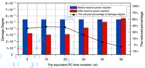
Figure 19.
Accumulated fatigue damage under various RC time constants for the IGBT module.
However, the fourth to sixth sets of data reveal the limitations of the algorithm. Specifically, selecting a large equivalent RC parameter in the algorithm results in excessive reactive power injection. This excessive injection leads to a significant rise in the average junction temperature of power devices, thereby compromising the effectiveness of the algorithm in improving reliability. The trade-off between suppressing power fluctuations and maintaining a low average junction temperature becomes more evident as the equivalent RC parameter increases. Hence, it is crucial to carefully select the appropriate value of the equivalent RC parameter to achieve a balance between reducing power fluctuations and maintaining a reasonable average junction temperature for optimal device reliability.
By precisely adjusting the amount of reactive power injection, it is possible to attain the best performance of the algorithm for a specific power fluctuation scenario. Further analysis and experiments are necessary to determine the optimal amount of reactive power injection for different power fluctuation conditions, considering the trade-off between power fluctuation suppression and average junction temperature increase. This optimization process can maximize the reliability enhancement provided by the algorithm while minimizing potential drawbacks.
6. Conclusions
Long-term complex power fluctuations imposed on the converter result in heightened thermal stress between material layers of the module, which increases the risk of failure in power devices and presents a significant challenge to the reliable operation of the microgrid. This paper presents a proposed reactive power injection algorithm with the objective of mitigating power fluctuations. The simulation results demonstrate that when examining the impact of the algorithm under various power fluctuation scenarios while maintaining a constant equivalent RC time constant of 22.5 s, the algorithm achieves its highest effectiveness when the active power fluctuates between 10 kW and 80 kW. In this range, the algorithm successfully enhances the lifetime of the power device by 74.13%. During the examination of the algorithm’s impact under varying reactive power injection amounts, it is observed that the algorithm achieves optimal effectiveness when the active power fluctuates between 40 kW and 80 kW, and the equivalent RC time constant is set to 15 s. Under these conditions, the algorithm successfully improves the lifetime of the power device by 43.03%. The results of this study highlight the notable contribution of the proposed algorithm in reliability enhancement.
The key contribution of this study is presenting a reliability enhancement strategy that utilizes apparent power reconstruction to mitigate power fluctuation. A novel reactive power injection algorithm is also employed at the converter control level in the implementation process. The proposed algorithm in this study provides distinct advantages over the device-level, converter-level, and system-level reliability management methods mentioned. It eliminates the requirement for intricate adjustments in the control loop, drive circuit, and EMI suppression, resulting in a straightforward implementation with minimal risk. Additionally, it surpasses converter-level approaches by efficiently modifying the pattern of output power fluctuation and mitigating deep cycling in junction temperature. Moreover, unlike system-level algorithms, the proposed method exhibits adaptability to diverse working scenarios involving converters and different micro sources, offering flexibility and versatility. However, the method still exhibits the following limitations:
- (1)
- The utilization of reactive power injection effectively mitigates the power fluctuations in the converter, thereby enhancing the reliability of microgrid operation to a certain extent. However, it does affect the power distribution from the converter to the system. Hence, it becomes necessary to implement further coordinated management of the converters corresponding to different micro sources within the system, which aims to ensure the power delivery requirement and enhance the operational reliability of the microgrid system.
- (2)
- The proposed reactive power injection algorithm mitigates junction temperature fluctuations while increasing the average junction temperature concurrently, which presents a challenge to the reliability of power devices. Therefore, further theoretical research is needed to investigate the effect of power fluctuation on the reliability of power devices, eventually achieving an accurate calculation of reactive power injection amount based on the power fluctuation for the purpose of improving power devices’ reliability.
- (3)
- The verification procedure solely consists of simulations; therefore, it is crucial to construct an experimental platform to further validate the feasibility of the proposed algorithm.
Author Contributions
Conceptualization, B.L. and H.L.; methodology, B.L.; software, H.L.; validation, H.L.; formal analysis, H.L.; investigation, B.L.; resources, H.Z.; data curation, M.H.; writing—original draft preparation, B.L.; writing—review and editing, H.L.; visualization, M.H.; supervision, B.L.; project administration, B.L.; funding acquisition, H.Z. All authors have read and agreed to the published version of the manuscript.
Funding
This work was supported by the Natural Science Foundation of Shaanxi Province, China (2023-JC-YB-381).
Data Availability Statement
Data is contained within the article.
Conflicts of Interest
The authors declare no conflict of interest.
Abbreviations
The following abbreviations are used in this manuscript:
| IGBTs | Insulated gate bipolar transistors |
| FWD | Freewheeling diode |
| DSVPWM | Discontinuous space vector pulse width modulation |
| DPWM | Discontinuous pulse width modulation |
| CPWM | Continuous pulse width modulation |
| EMI | Electromagnetic interference |
| PNR | Power network reconfiguration |
| SNS | Social network search |
| MJFS | Modified jellyfish search |
| ONR | Optimal network reconfiguration |
| MG | Microgrid |
| EO | Equilibrium optimization |
| CTE | Coefficients of thermal expansion |
References
- Guo, L.; Wang, W.; Liu, W.; Jiao, B.; Wang, C.; Liu, Y.; Wang, S. The Energy Management Method for Stand-Alone Wind/Diesel/Battery/Sea-Water Desalination Microgrid. Trans. China. Electrotech. Soc. 2014, 29, 113–121. [Google Scholar]
- Barzkar, A.; Ghassemi, M. Electric Power Systems in More and All Electric Aircraft: A Review. IEEE Access 2020, 8, 169314–169332. [Google Scholar] [CrossRef]
- Sulligoi, G.; Vicenzutti, A.; Menis, R. All-Electric Ship Design: From Electrical Propulsion to Integrated Electrical and Electronic Power Systems. IEEE Trans. Transp. Electrif. 2016, 2, 507–521. [Google Scholar] [CrossRef]
- Zheng, S.; Du, X.; Zhang, J.; Yu, Y.; Sun, P. Measurement of Thermal Parameters of SiC MOSFET Module by Case Temperature. IEEE. J. EM. Sel. Top. P. 2020, 8, 311–322. [Google Scholar] [CrossRef]
- Yang, Z.; Zhou, L.; Du, X.; Sun, P.; Mao, Y. Effects of Different Parameters on Reliability of Grid-side Converters Based on Varied Junction Temperature of Devices in Wind Turbines. Proc. Chin. Soc. Electr. Eng. 2013, 33, 41–49+8. [Google Scholar]
- Wang, H.; Liserre, M.; Blaabjerg, F.; Jacobsen, J.B.; Kvisgaard, T.; Landkildehus, J. Transitioning to Physics-of-Failure as a Reliability Driver in Power Electronics. IEEE J. Emerg. Sel. Top. Power Electron. 2014, 2, 97–114. [Google Scholar] [CrossRef]
- Ma, K.; Liserre, M.; Blaabjerg, F.; Kerekes, T. Thermal Loading and Lifetime Estimation for Power Device Considering Mission Profiles in Wind Power Converter. IEEE Trans. Power Electron. 2015, 30, 590–602. [Google Scholar] [CrossRef]
- Rodriguez, C.; Amaratunga, G.A.J. Long-Lifetime Power Inverter for Photovoltaic AC Modules. IEEE Trans. Ind. Electron. 2008, 55, 2593–2601. [Google Scholar] [CrossRef]
- Chan, F.; Calleja, H. Reliability Estimation of Three Single-Phase Topologies in Grid-Connected PV Systems. IEEE Trans. Ind. Electron. 2011, 58, 2683–2689. [Google Scholar] [CrossRef]
- Harb, S.; Balog, R.S. Reliability of Candidate Photovoltaic Module-Integrated-Inverter (PV-MII) Topologies—A Usage Model Approach. IEEE Trans. Power Electron. 2013, 28, 3019–3027. [Google Scholar] [CrossRef]
- Mukherjee, N.; Strickland, D. Second Life Battery Energy Storage Systems: Converter topology and redundancy selection. In Proceedings of the 7th IET International Conference on Power Electronics, Machines and Drives (PEMD 2014), Manchester, UK, 8–10 April 2014; pp. 1–6. [Google Scholar]
- Ma, K.; Wang, H.; Blaabjerg, F. New Approaches to Reliability Assessment: Using physics-of-failure for prediction and design in power electronics systems. IEEE Power Electron. Mag. 2016, 3, 28–41. [Google Scholar] [CrossRef]
- Flack, J.; Andresen, M.; Liserre, M. Active Thermal Control of IGBT Power Electronic Converters. In Proceedings of the IECON 2015—41st Annual Conference of the IEEE Industrial Electronics Society, Yokohama, Japan, 9–12 November 2015; pp. 1–6. [Google Scholar]
- Huang, S.; Chen, Y.; Liu, P.; Rong, F. Band-Oriented Active Thermal Management Control of PWM Inverter. Electr. Power. Autom. Equip. 2017, 37, 34–39. [Google Scholar]
- Hu, R.; Chen, Q.; Hu, C. Study on Thermal Reliability of Three-Level Inverter Based on Dynamic DSVPWM. Power Electron. 2019, 53, 87–89+107. [Google Scholar]
- Du, X.; Li, G.; Li, T.; Sun, P.; Zhou, L. A Hybrid Modulation Method for Improving the Lifetime of Power Modules in the Wind Power Converter. Proc. Chin. Soc. Electr. Eng. 2015, 35, 5003–5012. [Google Scholar]
- Sathik, M.H.M.; Prasanth, S.; Sasongko, F.; Padmanabhan, S.K.; Pou, J.; Simanjorang, R. A Dynamic Thermal Controller for Power Semiconductor Devices. In Proceedings of the 2018 IEEE Applied Power Electronics Conference and Exposition (APEC), San Antonio, TX, USA, 4–8 March 2018; pp. 2792–2797. [Google Scholar]
- Wang, B.; Zhou, L.; Zhang, Y.; Wang, K.; Du, X.; Sun, P. Active Junction Temperature Control of IGBT Based on Adjusting the Turn-off Trajectory. IEEE Trans. Power Electron. 2018, 33, 5811–5823. [Google Scholar] [CrossRef]
- Liserre, M.; Andresen, M.; Costa, L.; Buticchi, G. Power Routing in Modular Smart Transformers: Active Thermal Control Through Uneven Loading of Cells. IEEE Ind. Electron. Mag. 2016, 10, 43–53. [Google Scholar] [CrossRef]
- Buticchi, G.; Andresen, M.; Wutti, M.; Liserre, M. Lifetime-Based Power Routing of a Quadruple Active Bridge DC/DC Converter. IEEE Trans. Power Electron. 2017, 32, 8892–8903. [Google Scholar] [CrossRef]
- Shaheen, A.; El-Sehiemy, R.; Kamel, S.; Selim, A. Optimal Operational Reliability and Reconfiguration of Electrical Distribution Network Based on Jellyfish Search Algorithm. Energies 2022, 15, 6994. [Google Scholar] [CrossRef]
- Shaheen, A.; El-Sehiemy, R.; Kamel, S.; Selim, A. Reliability Improvement Based Reconfiguration of Distribution Networks via Social Network Search Algorithm. In Proceedings of the 2022 23rd International Middle East Power Systems Conference (MEPCON), Cairo, Egypt, 13–15 December 2022; pp. 1–6. [Google Scholar]
- Shaheen, A.; El-Seheimy, R.; Kamel, S.; Selim, A. Reliability enhancement and power loss reduction in medium voltage distribution feeders using modified jellyfish optimization. Alex. Eng. J. 2023, 75, 363–381. [Google Scholar] [CrossRef]
- Abou El-Ela, A.A.; El-Sehiemy, R.A.; Allam, S.M.; Shaheen, A.M.; Nagem, N.A.; Sharaf, A.M. Renewable Energy Micro-Grid Interfacing: Economic and Environmental Issues. Electronics 2022, 11, 815. [Google Scholar] [CrossRef]
- Ma, K.; Liserre, M.; Blaabjerg, F. Reactive Power Influence on the Thermal Cycling of Multi-MW Wind Power Inverter. IEEE Trans. Ind. Appl. 2013, 49, 922–930. [Google Scholar] [CrossRef]
- Wan, S. Thermal Behavior Optimal Control for Wind Power Converter with Reactive Power Circulation. Electric Drive 2017, 47, 68–74. [Google Scholar]
- Jauhari, M.; Riawan, D.C.; Ashari, M. Control Design for Shunt Active Power Filter Based on PQ Theory in Photovoltaic Grid-Connected System. Int. J. Power Electron. Drive Syst. 2018, 9, 1064–1071. [Google Scholar]
- Haider, S.; Li, G.; Wang, K. A dual control strategy for power sharing improvement in islanded mode of AC microgrid. Prot Control Mod Power Syst. 2018, 3, 10. [Google Scholar] [CrossRef]
- An, T.; Zhou, R.; Qin, F.; Dai, Y.; Gong, Y.; Chen, P. Comparative Study of the Parameter Acquisition Methods for the Cauer Thermal Network Model of an IGBT Module. Electronics 2023, 12, 1650. [Google Scholar] [CrossRef]
- Sun, P.; Wang, H.; Gong, C.; Du, X.; Luo, Q.; Wang, Z. Mechanism Research of Short-circuit Current as Bond Wire Ageing Indicator of Insulated Gate Bipolar Transistor Module. Proc. Chin. Soc. Electr. Eng. 2019, 39, 4876–4883+4989. [Google Scholar]
- Wang, X.; Zhang, B.; Wu, H. A Review of Fatigue Mechanism of Power Devices Based on Physics-of-Failure. Trans. China. Electrotech. Soc. 2019, 34, 717–727. [Google Scholar]
- Choi, U.M.; Blaabjerg, F.; Lee, K.B. Study and Handling Methods of Power IGBT Module Failures in Power Electronic Converter Systems. IEEE Trans. Power Electron. 2015, 30, 2517–2533. [Google Scholar] [CrossRef]
- Choi, U.M.; Blaabjerg, F.; Jørgensen, S. Study on Effect of Junction Temperature Swing Duration on Lifetime of Transfer Molded Power IGBT Modules. IEEE Trans. Power Electron. 2017, 32, 6434–6443. [Google Scholar] [CrossRef]
- Chang, L. Study on Principle and Distortion of Diode Envelope Detection Circuit. Electron. Test 2013, 17, 34–36. [Google Scholar]
- Li, L.; Xu, Y.; Li, Z. Calculation Method of IGBT Module Junction Temperature Based on Electro-thermal Coupling Model. J. Power Supply 2016, 14, 23–28. [Google Scholar]
- Liu, B.; Wang, G.; Tseng, M.; Wu, K.; Li, Z. Exploring the Electro-Thermal Parameters of Reliable Power Modules: Insulated Gate Bipolar Transistor Junction and Case Temperature. Energies 2018, 11, 2371. [Google Scholar] [CrossRef]
- Hafezi, H.; Faranda, R. A New Approach for Power Losses Evaluation of IGBT/Diode Module. Electronics 2021, 10, 280. [Google Scholar] [CrossRef]
- Yang, X.; Zhai, X.; Long, S.; Li, M.; Dong, H.; He, Y. Insulated Gate Bipolar Transistor Reliability Study Based on Electro-Thermal Coupling Simulation. Electronics 2023, 12, 2116. [Google Scholar] [CrossRef]
- Fan, X.; Wang, Y.; Li, W. Modeling and Analysis of IGBT Power Module Electro-thermal Coupling Model. In Proceedings of the 2021 IEEE 4th International Electrical and Energy Conference (CIEEC), Wuhan, China, 28–30 May 2021; pp. 1–6. [Google Scholar]
- Shuai, S.; Xiong, W.; Peng, Y.; Ai, X.; Liu, Y.; Zhu, L. IGBT Reliability Evaluation Based on Electro-thermal Coupling Model and Life Prediction. Electr. Power Sci. Eng. 2021, 37, 17–25. [Google Scholar]
- Li, G.; Du, X.; Sun, P.; Zhou, L.; Tai, H. Numerical IGBT junction temperature calculation method for lifetime estimation of power semiconductors in the wind power converters. In Proceedings of the 2014 International Power Electronics and Application Conference and Exposition, Shanghai, China, 5–8 November 2014; pp. 49–55. [Google Scholar]
- Bouzida, A.; Abdelli, R.; Ouadah, M. Calculation of IGBT power losses and junction temperature in inverter drive. In Proceedings of the 2016 8th International Conference on Modelling, Identification and Control (ICMIC), Algiers, Algeria, 15–17 November 2016; pp. 768–773. [Google Scholar]
- Ma, K.; Liserre, M.; Blaabjerg, F. Reactive power control methods for improved reliability of wind power inverters under wind speed variations. In Proceedings of the 2012 IEEE Energy Conversion Congress and Exposition (ECCE), Raleigh, NC, USA, 15–20 September 2012; pp. 3105–3112. [Google Scholar]
- Zheng, H.; Wang, X.; Wang, X.; Ran, L.; Zhang, B. Using SiC MOSFETs to improve reliability of EV inverters. In Proceedings of the 2015 IEEE 3rd Workshop on Wide Bandgap Power Devices and Applications (WiPDA), Blacksburg, VA, USA, 2–4 November 2015; pp. 359–364. [Google Scholar]
- Lin, S.; Fang, X.; Lin, F.; Yang, Z.; Wang, X.; Taku, T. Lifetime Prediction of IGBT Modules Based on Mission Profiles in Traction Inverter Application. In Proceedings of the 2019 IEEE Vehicle Power and Propulsion Conference (VPPC), Hanoi, Vietnam, 14–17 October 2019; pp. 1–6. [Google Scholar]
- GopiReddy, L.; Tolbert, M.; Ozpineci, B. Lifetime prediction of IGBT in a STATCOM using modified-graphical rainflow counting algorithm. In Proceedings of the IECON 2012—38th Annual Conference on IEEE Industrial Electronics Society, Montreal, QC, Canada, 25–28 October 2012; pp. 3425–3430. [Google Scholar]
- Cheng, T.; Lu, D.; Siwakoti, Y.P. Circuit-Based Rainflow Counting Algorithm in Application of Power Device Lifetime Estimation. Energies 2022, 15, 5159. [Google Scholar] [CrossRef]
- Chen, Z.; Gao, F.; Yang, C.; Peng, T.; Zhou, L.; Yang, C. Converter Lifetime Modeling Based on Online Rainflow Counting Algorithm. In Proceedings of the 2019 IEEE 28th International Symposium on Industrial Electronics (ISIE), Vancouver, BC, Canada, 12–14 June 2019; pp. 1743–1748. [Google Scholar]
- GopiReddy, L.R.; Tolbert, L.M.; Ozpineci, B.; Pinto, J.O.P. Rainflow Algorithm-Based Lifetime Estimation of Power Semiconductors in Utility Applications. IEEE Trans. Ind. Appl. 2015, 51, 3368–3375. [Google Scholar] [CrossRef]
- Bryant, A.T.; Mawby, P.A.; Palmer, P.R.; Santi, E.; Hudgins, J.L. Exploration of Power Device Reliability Using Compact Device Models and Fast Electrothermal Simulation. IEEE Trans. Ind. Appl. 2008, 44, 894–903. [Google Scholar] [CrossRef]
- Nguyen, M.H.; Kwak, S. Enhance Reliability of Semiconductor Devices in Power Converters. Electronics 2020, 9, 2068. [Google Scholar] [CrossRef]
- Wang, C.; He, Y.; Wang, C.; Wu, X.; Li, L. A Fusion Algorithm for Online Reliability Evaluation of Microgrid Inverter IGBT. Electronics 2020, 9, 1294. [Google Scholar] [CrossRef]
Disclaimer/Publisher’s Note: The statements, opinions and data contained in all publications are solely those of the individual author(s) and contributor(s) and not of MDPI and/or the editor(s). MDPI and/or the editor(s) disclaim responsibility for any injury to people or property resulting from any ideas, methods, instructions or products referred to in the content. |
© 2023 by the authors. Licensee MDPI, Basel, Switzerland. This article is an open access article distributed under the terms and conditions of the Creative Commons Attribution (CC BY) license (https://creativecommons.org/licenses/by/4.0/).