Article

A High Performance Reconfigurable Hardware Architecture for Lightweight Convolutional Neural Network

1
School of Microelectronics, Fudan University, Shanghai 200433, China
2
Institute of Big Data, Fudan University, Shanghai 200433, China
*
Authors to whom correspondence should be addressed.
Electronics 2023, 12(13), 2847; https://doi.org/10.3390/electronics12132847
Submission received: 9 June 2023 / Revised: 22 June 2023 / Accepted: 23 June 2023 / Published: 27 June 2023
(This article belongs to the Section Artificial Intelligence Circuits and Systems (AICAS))

Abstract

:
Since the lightweight convolutional neural network EfficientNet was proposed by Google in 2019, the series of models have quickly become very popular due to their superior performance with a small number of parameters. However, the existing convolutional neural network hardware accelerators for EfficientNet still have much room to improve the performance of the depthwise convolution, squeeze-and-excitation module and nonlinear activation functions. In this paper, we first design a reconfigurable register array and computational kernel to accelerate the depthwise convolution. Next, we propose a vector unit to implement the nonlinear activation functions and the scale operation. An exchangeable-sequence dual-computational kernel architecture is proposed to improve the performance and the utilization. In addition, the memory architectures are designed to complete the hardware accelerator for the above computing architecture. Finally, in order to evaluate the performance of the hardware accelerator, the accelerator is implemented based on Xilinx XCVU37P. The results show that the proposed accelerator can work at the main system clock frequency of 300 MHz with the DSP kernel at 600 MHz. The performance of EfficientNet-B3 in our architecture can reach 69.50 FPS and 255.22 GOPS. Compared with the latest EfficientNet-B3 accelerator, which uses the same FPGA development board, the accelerator proposed in this paper can achieve a 1.28-fold improvement of single-core performance and 1.38-fold improvement of performance of each DSP.

1. Introduction

As the requirements for high accuracy and the computational complexities of convolutional neural network (CNN) models continue to increase, CNNs gradually show a trend of greater depth, more complex structures and more parameters, which bring great challenges to their deployment on hardware platforms with limited hardware resources. To solve the above problems, lightweight convolutional neural network models and customized convolutional neural network hardware architectures have become very popular.
Lightweight neural networks usually use the depthwise convolutions (DWC) to decouple parts of the standard convolutions (STC), such as ShuffleNets [1,2], MobileNets [3,4,5] and MnasNet [6]. The EfficientNet series networks [7,8], which were firstly proposed by Google, are one of the best lightweight neural networks. Neural Architecture Search (NAS) [6] is used to search for the optimal configuration of the network, and eight scaling versions of B0-B7 are proposed. EfficientNet-B7 achieves a high accuracy rate of 84.3% in the Top-1 ImageNet classification tasks. Compared with GPipe [9], the number of parameters of EfficientNet-B7 is only 11.9% of GPipe.
Although the performance of EfficientNet is excellent, there is a gap between its algorithm modeling and its hardware implementation. According to the public data on the official website of NVIDIA [10] and the estimates of Multiply-Accumulate (MAC) Operation numbers, when inferring ResNet-50, a standard convolutional neural network with the data type of INT8, the computing resource utilization of ResNet-50 on NVIDIA A100 is about 21.4%. However, the computing resource utilization is only 2.1% when inferring EfficientNet-B0. Therefore, the utilization of computing resource on GPU of EfficientNet is much lower than that of traditional convolutional neural networks.
FPGAs have the advantages of flexibility and energy efficiency compared with other general-purpose platforms and can use dedicated DSP slices to further improve the computing performance. As a result, CNN hardware accelerators based on the FPGA hardware platform are being increasingly focused upon by researchers. CNN hardware accelerators based on FPGA can be divided into training accelerators [11,12] and inference accelerators [13,14,15]. Our work mainly focuses on the FPGA inference accelerator.
In recent years, hardware accelerators for lightweight CNNs have made some progress. In [16,17,18,19,20], the authors mainly accelerate MobileNetV1 or MobileNetV2, which lack the 5 × 5 DWC, squeeze-and-excitation (SE) module and complex nonlinear activation functions (NAF). In [21,22], the authors accelerate EfficientNet-lite, which is a simplified version of the EfficientNet series models and also lacks the implementations of the SE module and complex NAF. In [23], the author can only accelerate EfficientNet-B0 without the implementations of DWC and NAF and cannot support other versions of EfficientNet series models because of its customized pipelined architecture. In [24], a hardware/software co-optimizer is proposed to provide adaptive data reuses to minimize the off-chip memory access and improve the MAC efficiency with the on-chip buffer constraints and accelerate EfficientNet-B1 with 2240 DSP slices. In [25], EfficientNet series models are supported, but the accelerator has a poor performance for DWC because of the parallel strategy. In summary, the existing FPGA accelerators cannot support both standard convolution and depthwise convolution efficiently because the parallel strategies are different between DWC and STC. Furthermore, they are not efficient enough to accelerate the squeeze-and-excitation module and nonlinear activation functions in EfficientNet. There is much room to improve the performance of hardware accelerators for EfficientNet series models.
The contributions of this work are as follows:
  • An FPGA-based computational kernel and a reconfigurable register array are proposed to improve the utilization of computing resources for the depthwise convolution.
  • A vector unit is designed to implement the nonlinear activation functions and the scale operation in the SE module.
  • An exchangeable-sequence dual-computational kernel architecture and its memory architectures are designed to improve the performance and utilization.
The rest of this paper is structured as follows. Section 2 introduces the background and related work. Section 3 introduces the analysis of design space. Furthermore, Section 4 describes the proposed hardware architecture. Section 5 shows the experimental results, and Section 6 concludes the paper.

2. Background and Related Work

2.1. Lightweight Convolutional Neural Network

Depthwise separable convolution, which combines depthwise convolution and pointwise convolution, was first proposed by Sifre L. [26] in his Ph.D. thesis, who deduced its theoretical principle in detail. Subsequently, Chollet F. [27] proposed Xception by combining the depthwise separable convolution and Inception V3 [28]. Xception has a slight accuracy advantage over Inception V3 on the ImageNet dataset with a similar number of parameters. Since then, lightweight neural networks [1,2,3,4,5,6,7,8] have become hot topics in artificial intelligence.
EfficientNet series models, one of the best lightweight CNNs, consist of the parameterized mobile inverted bottleneck convolution (MBCONV) module with the squeeze-and-excitation (SE) module, which is shown in Figure 1. Expand Convolution, Squeeze, Excitation and Project Convolution are 1 × 1 standard convolutions, which can employ multiply-accumulate parallelism along the input channels. Depthwise convolutions in EfficientNet are 3 × 3 and 5 × 5, which do not accumulate along the input channels. It is worth noting that the scale operation in the SE module is equivalent to 1 × 1 depthwise convolution. For ease of presentation, we refer to the datapath before the global pooling as the input of the scale operation and the datapath after the global pooling as the weight of the scale operation, which are shown in Figure 1. Furthermore, if the input size is equal to the output size of MBCONV, the output feature map of MBCONV will add the input feature map in the end, which is called Branch Add.

2.2. Existing Hardware Architectures for Lightweight CNNs

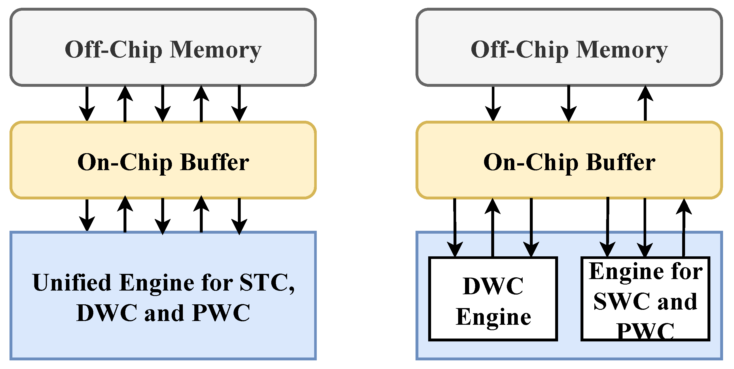
The early lightweight neural network hardware accelerators in academia were mainly used to accelerate MobileNets. The separated engine architecture and unified engine architecture, which are shown in Figure 2, are two common lightweight CNN hardware accelerator architectures.
For the unified engine architecture, all types of convolution computation are performed in a unified engine of computation. In [17], a line buffer architecture is proposed to support the 3 × 3 DWC in MobileNetV2, which is not efficient for the 5 × 5 DWC or scale operation in EfficientNet. LETA [25] is a typical unified engine architecture. Although it can support standard convolutions very well, it has poor performance for depthwise convolutions in EfficientNet. Furthermore, LETA cannot support nonlinear activation functions and the scale operation efficiently. In [22], a new systolic array for depthwise convolutions is proposed based on ASIC implementation with a much higher frequency than FPGA. The performance of depthwise convolutions is better than that of other traditional systolic arrays, but it can only support EfficientNet-lite efficiently, which lacks the SE module and complex nonlinear activation functions.
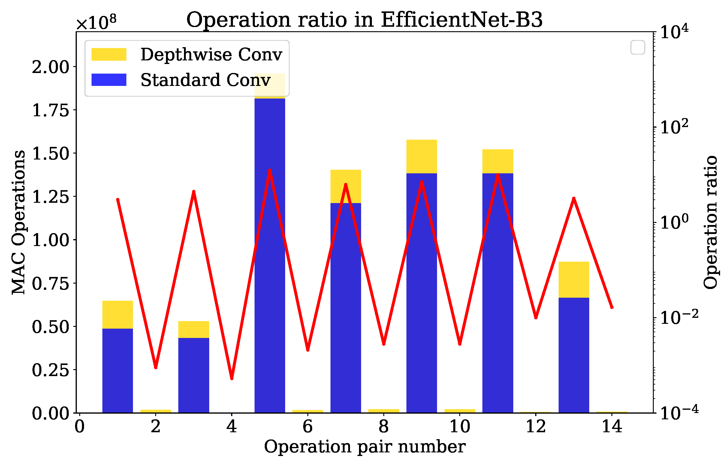
For the separated engine architecture, the standard convolution engine and the depthwise convolution engine will form a pipeline to work. It also needs the balance of MAC numbers of adjacent standard convolution and depthwise convolution. This method, which is used in [16], is more suitable for MobileNetV2 but not suitable for EfficientNet. The MAC numbers of the standard convolution and the depthwise convolution of the first 14 operation pairs in EfficientNet-B3 are shown in Figure 3. We can find that the ratio fluctuates sharply due to the difference between the SE module in MBCONV and other traditional depthwise separable convolutions. The pipeline cannot be formed very well because of the imbalanced workload of two different engines. In a word, both the traditional separated engine and unified engine cannot support EfficientNet series models efficiently.

3. Design Space Analysis

3.1. Parallel Strategies Analysis

Different parallel strategies correspond to different data flows and different hardware architectures. In lightweight convolutional neural networks, standard convolutions account for the majority of computation, and pointwise convolutions are the major computational components of standard convolutions. Considering that the numbers of input channels and output channels of pointwise convolutions are very large integer multiples of 16 or 32, in academia, 16 × 16 or 32 × 32 computational arrays are often designed. In addition, pointwise convolutions are difficult to parallel on the kernel dimension, so it is natural to parallel on the input channel and output channel dimensions.
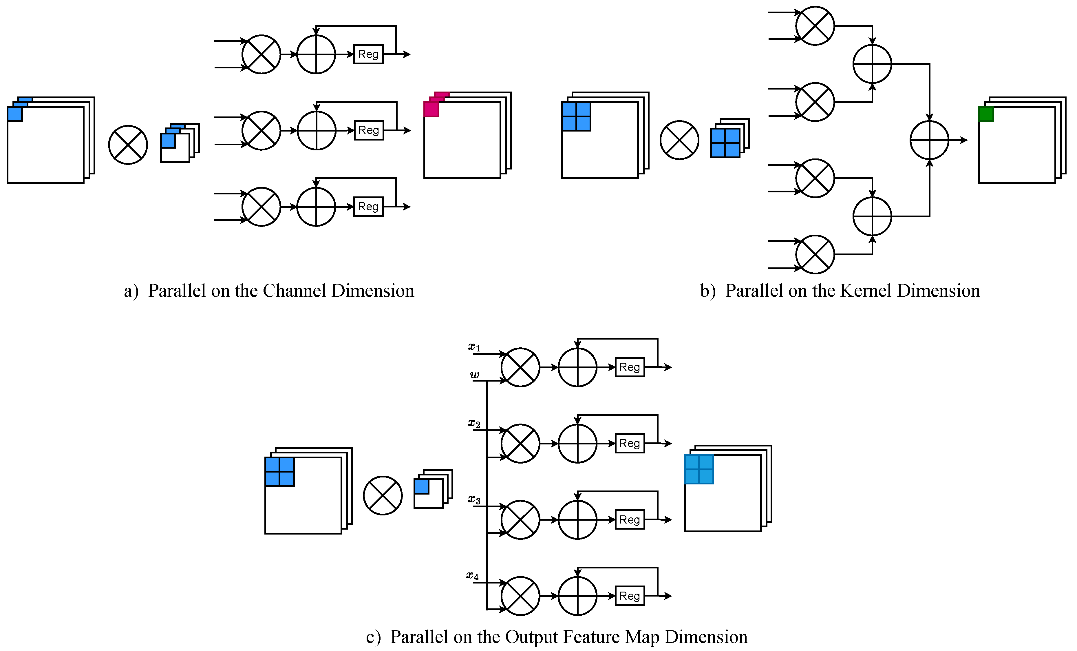
According to the computational characteristics of the depthwise convolution, the 16 × 16 or 32 × 32 computational arrays cannot be paralleled simultaneously on the input channel and output channel dimensions. Three parallel strategies commonly used for DWC are shown in Figure 4.
In addition to parallelism on the channel dimensions, it is natural to adopt the parallel strategy of the output feature map dimension or the convolutional kernel dimension. The pros and cons of these two strategies can be evaluated by a typical MBCONV module. The stride of the depthwise convolution of MBCONV is usually equal to one, and 3 × 3 DWC is the most common DWC in the EfficientNet series models. We can assume that the input sizes of expand convolution, depthwise convolution, the scale operation and project convolution are H · W . Assuming that the input channel number of expand convolution is C 1 , the output channel number is C 2 , meaning that the numbers of the input channel and output channel of the depthwise convolution and scale operation are C 2 . The numbers of input and output channels of project convolution are C 2 and C 3 . In general, C 3 is usually equal to C 1 . Our single-core computational array uses 32 × 32 multipliers with the INT8 quantization method. The parallelisms of the input channel and output channel of our computational array are I C P and O C P , respectively. The number of theoretical computation clock cycles of expand convolution at the first layer is
T e x p = H · W · C 1 · C 2 I C P · O C P
Assuming that the depthwise convolution is paralleled on the output feature map and the degree of parallelism is N, the number of computation cycles of the depthwise convolution is
T d p w 1 = H · W · K 2 · C 2 N · I C P
In another situation, it is assumed that parallelism is not performed on the output feature map but on the convolution kernel. The number of computation cycles in this case is
T d p w 2 = H · W · C 2 I C P
The scale operation is equivalent to the depthwise convolution with a 1 × 1 kernel. In the case of channel parallelism, the number of computation cycles of the scale operation is
T s c a l e = H · W · C 2 I C P
The number of computation cycles of project convolution is the same as that of expand convolution when C 3 = C 1 :
T p r o = H · W · C 2 · C 1 I C P · O C P
The numbers of clock cycles of squeeze and excitation, which are small percentages in MBCONV, can be ignored in the rough estimation. The number of clock cycles of MBCONV of the output feature map parallel strategy is
T n u m 1 = H · W · 2 · C 2 · C 1 I C P · O C P + K 2 · C 2 N · I C P + C 2 I C P
The number of clock cycles of MBCONV of the kernel parallel strategy is
T n u m 2 = H · W · 2 · C 2 · C 1 I C P · O C P + 2 · C 2 I C P
Assuming that the computation resource utilization of output feature map parallelism is U 1 and that of kernel parallelism is U 2 , then the ratio of computing resource utilization in the above two cases is
η = U 2 U 1 = T n u m 1 T n u m 2 = H · W · 2 · C 2 · C 1 I C P · O C P + K 2 · C 2 N · I C P + C 2 I C P H · W · 2 · C 2 · C 1 I C P · O C P + 2 · C 2 I C P = 2 · C 1 O C P + K 2 N + 1 2 · C 1 O C P + 2
Because of the bandwidth limitation, parallelism on the output feature map dimension must be satisfied: K 2 N 1 . Then, the ratio of computing resource utilization in the above two cases is
η = 2 · C 1 O C P + K 2 N + 1 2 · C 1 O C P + 2 1
In summary, parallelism on the kernel dimension can definitely improve the performance and utilization of the hardware accelerator.

3.2. Architecture Analysis

In addition, in contrast to the traditional lightweight convolutional neural networks, there is a special SE module both in the latest EfficientNet series models and MobileNetV3 [5]. The scale operation in the SE module can be equivalent to the depthwise convolution with a 1 × 1 kernel. Although the computation number of the scale operation is not large, it is difficult to make full use of it on the existing computational arrays such as 16 × 16 and 32 × 32. The multiplication number of the scale operation is H · W · C 2 . The number of multiplications of project convolution after the scale operation is H · W · C 2 · C 1 . It is worth noting that C 2 is usually six or four times as much as C 1 .
If a vector unit with fewer hardware resources is designed and the scale operation is processed separately, the computing clock cycles of the scale operation can be covered by the project convolution processed in the traditional computational array, and the scale operation and project convolution in hardware can be pipelined. The number of clock cycles of MBCONV in the kernel parallel strategy becomes
T n u m 3 = H · W · 2 · C 2 · C 1 I C P · O C P + C 2 I C P < T n u m 2
Then, we can further improve the performance of the accelerator.

4. Hardware Architecture Design

4.1. Architecture Overview

The system hardware architecture of our work is shown in Figure 5, which mainly consists of the instruction controller, address controller, input and output buffer, input and output interface, computational kernel with weight caches, vector unit and pooling unit.
The instruction controller reads the instruction from the off-chip memory by means of DMA and stores the parsed instruction into the registers. Then, it can output the instruction to other modules and control the process of the data writing, computing and reading of the accelerator. The address controller can generate the addresses of input activation data, weight and other parameters.
The memories of our hardware accelerator include off-chip memory and on-chip memory. The computational modules mainly contain the computational array for convolution computation, the vector unit for nonlinear activation functions and the scale operation and the pooling unit for global average pooling. The input interface, which mainly includes the reconfigurable register array, reorganizes the input data and broadcasts them to the computational array according to different computing modes and configuration information. The output interface, which mainly includes the bandwidth conversion architecture, is used to reorganize the output data and send them to the output buffer.
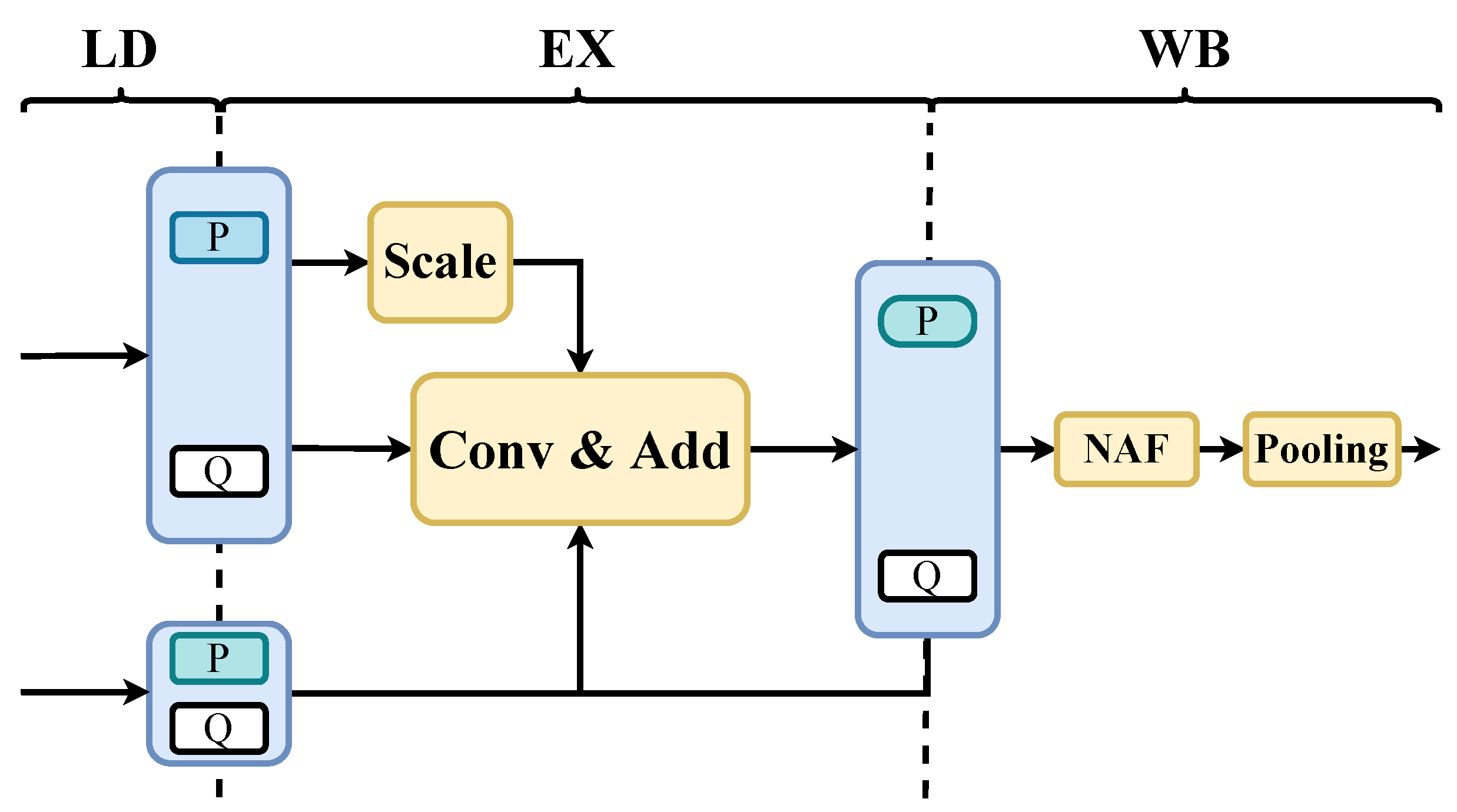
In order to improve the performance of hardware, we need to introduce the ping-pong buffer and pipeline each process of the hardware accelerator according to the on-chip memories. The pipeline of the accelerator can be divided into three levels: data loading (LD)→ execution (EX)→ data writing back (WB). The pipeline architecture of the proposed hardware accelerator is presented in Figure 6. Each round of computation performs a convolution operation of a data block and produces the intermediate or final results. According to the MBCONV structure in Figure 1, the scale operation before the convolution, or the nonlinear activation function and the global pooling after the convolution operation, are performed together in the same computation pipeline.

4.2. Computational Kernel and Register Array

Considering that standard convolutions are still the main parts of lightweight CNNs, the design of the computational kernel architecture should take accelerating standard convolution as the main goal; then, on this basis, it should be compatible with depthwise convolution efficiently. The DSP kernel [29] in Xilinx XCVU37P has a 27 × 18 multiplier and can compute the product of two individual factors and a shared factor in a system clock, which is called space-division multiplexing (SDM). In addition, the DSP kernel can run at twice the frequency of the main system, which is called time-division multiplexing (TDM). According to the previous research, the performance of standard convolution is limited by the computation roof rather than the communication roof in the Roofline model [30]. As a result, during STC, we should use SDM and TDM to make full use of the computing abilities. As shown in Figure 5, four groups of weights from four different output channels in a DSP unit are stored in four groups of weight caches, which are made by Distributed RAMs. We set 16 DSPs in a PE cell and 16 PEs in the computational kernel. The input data from 32 input channels are sent to the computational kernel. Adding the results of two adjacent PEs can make the input channel parallelism 32. Considering the SDM and TDM in STC, we can use 256 DSPs to implement a 32 × 32 INT8 multiplier array.
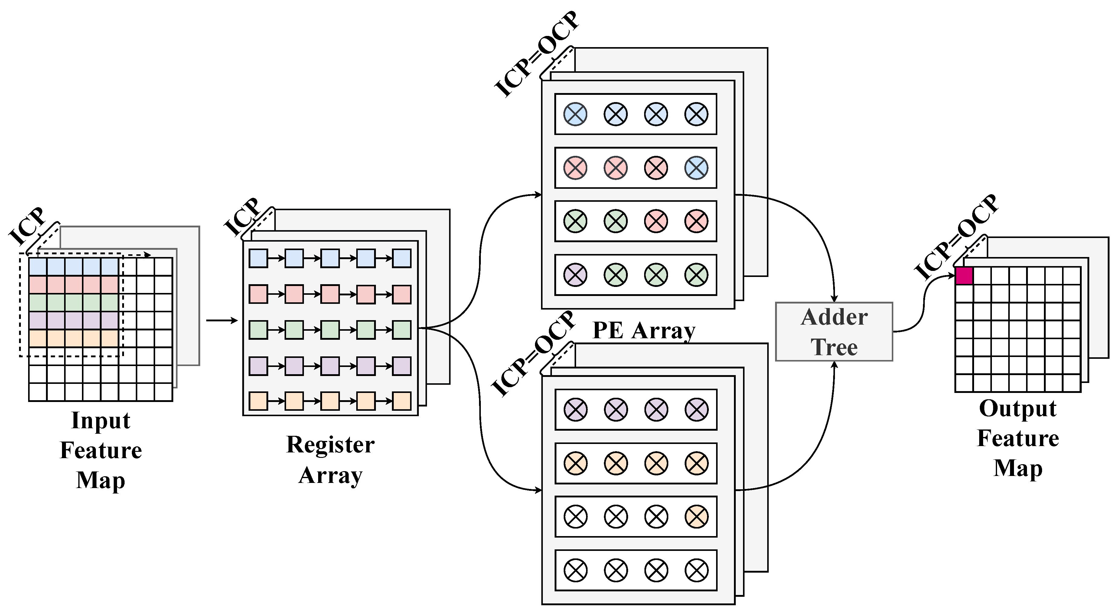
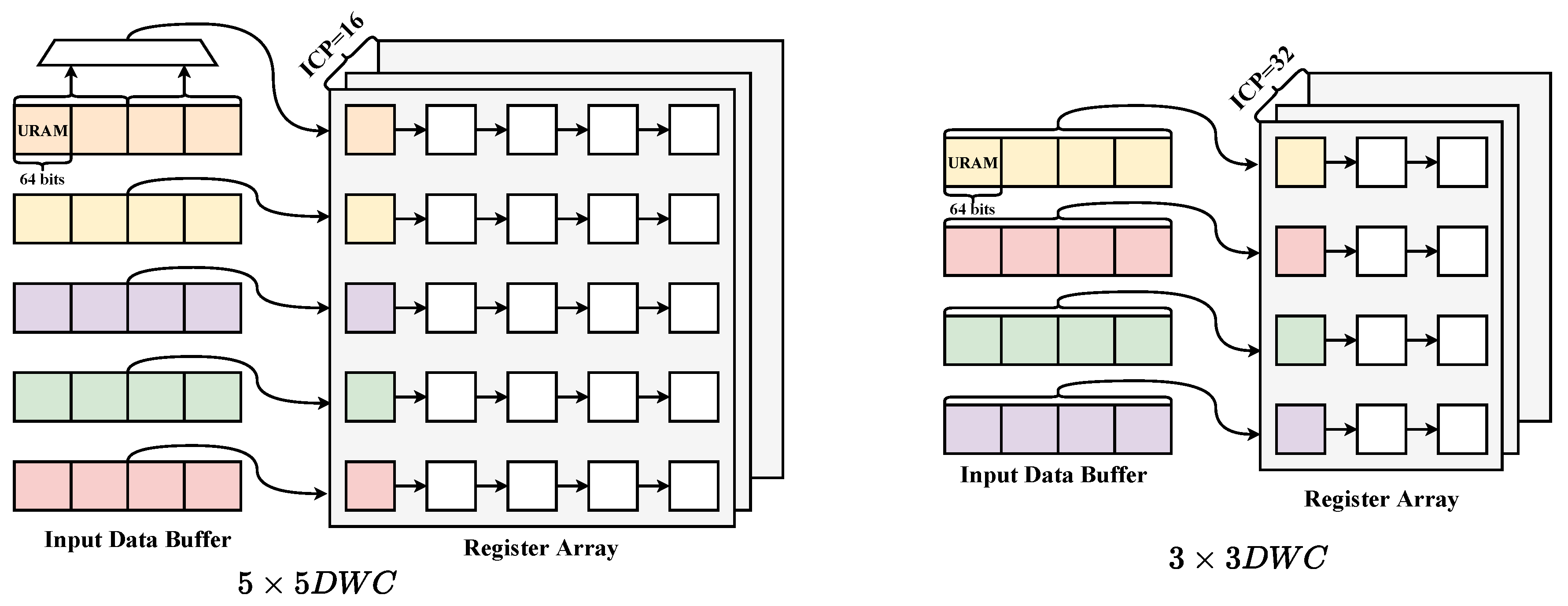
However, the design of the hardware accelerator for DWC requires a comprehensive consideration of the memory access and computing ability of the accelerator because the requirement of memory access of DWC is relatively more than that of STC. We set 25 registers to form a register array in the input interface module. The input buffer consists of five sub-memories and stores 5n, 5n + 1, 5n + 2, 5n + 3 and 5n + 4 rows of input feature map during the 5 × 5 DWC. We only use the TDM of the DSP, and the computing process of 5 × 5 DWC is shown in Figure 7.
At this time, the computational kernel can accept the data from 16 input channels, so the input channel parallelism is 16 and needs 16 × 5 × 5 registers in this register array. Two adjacent PEs can compute 25 products of data and weights. The bandwidth between the on-chip buffer (input buffer and output buffer) and the off-chip memory for DWC is 256 bits/cycle. Thus, we can calculate the theoretical clock cycles of the three-stage pipeline for 5 × 5 DWC with the stride of 1:
C l o c k C y c l e s o f L D = H · W · C i n · 8 b i t s 256 b i t s / c y c l e = H · W · C i n 32 C l o c k C y c l e s o f E X = H · W · C i n · 8 b i t s I C P · 8 b i t s / c y c l e = H · W · C i n 16 C l o c k C y c l e s o f W B = H · W · C o u t · 8 b i t s 256 b i t s / c y c l e = H · W · C o u t 32
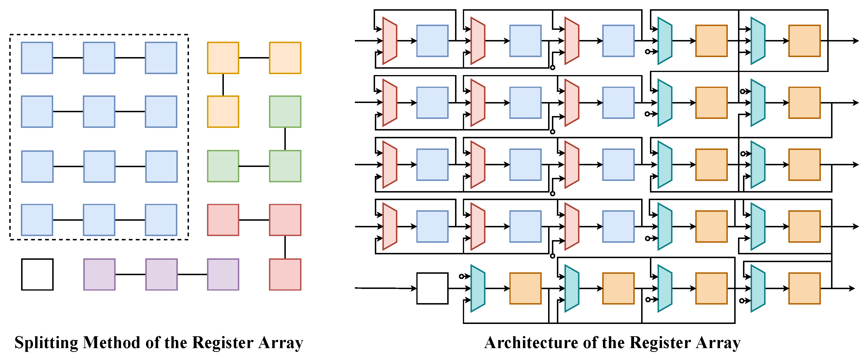
According to Equation (11), the number of clock cycles of EX is more than that of LD or WB. This means that the processes of LD and WB will not block the EX process during the 5 × 5 DWC. In addition, we need to note that 3 × 3 DWC accounts for the larger proportion in lightweight neural networks. During the 3 × 3 DWC, if only nine registers are used in a register array, more than half of the registers will be idle, and the parallelism of the input channel can only reach 16. This will lead to a loss of the utilization of hardware resources of FPGA. If the 2D register array of 5 × 5 can be split into two groups of 3 × 4 register arrays according to the splitting method of Figure 8, only one white register will be idle. The blue registers are the first group of the 3 × 4 register array, and the other colors together form the second group. Each three registers of the same color will form a register chain. At this time, the parallelism of the channels of 3 × 3 DWC will be increased by two times compared with the original architecture. Therefore, we can implement these two types of depthwise convolutions with two different channel parallelisms efficiently by configuring the register array. Another advantage of this design is that it can provide the bidirectional data transmission ability for 3 × 3 DWC, further avoiding cycle waste caused by the register chain during changing rows of input feature map.
The parallelism of the input channel of 3 × 3 DWC is 32, that is, 32 groups of 2D register arrays are connected to the data of 32 input channels, respectively, and each 2D register array transmits 9 valid pieces of data to a PE. We use TDM of DSP in DWC. The theoretical clock cycles of LD, EX and WB in the three-stage pipeline in the 3 × 3 DWC acceleration process are
C l o c k C y c l e s o f L D = H · W · C i n · 8 b i t s 256 b i t s / c y c l e = H · W · C i n 32 C l o c k C y c l e s o f E X = H · W · C i n · 8 b i t s I C P · 8 b i t s / c y c l e = H · W · C i n 32 C l o c k C y c l e s o f W B = H · W · C o u t · 8 b i t s 256 b i t s / c y c l e = H · W · C o u t 32
The number of clock cycles of LD is equal to that of EX or WB. This means the computing ability of the accelerator is in equilibrium with the memory access ability for 3 × 3 DWC. If we use the SDM and TDM together for DWC, the computing ability will increase. However, we need to add the bandwidth of the single-core accelerator, which will affect the numbers of multi-cores. As a result, only using the TDM of DSP for DWC can lead to equilibrium with the bandwidth. There are 1024 INT8 multipliers in the computational kernel in total while using TDM and SDM simultaneously. As a result, the theoretical utilization of the multipliers in the computational kernel during the 3 × 3 and 5 × 5 DWC with the stride of 1 are 9/32 and 25/64, respectively.

4.3. Vector Unit

Nonlinear activation functions in lightweight convolutional neural networks need to be implemented separately. In this paper, we reference the method of the piecewise linear (PWL) approximation in [31]. By observing the symmetry of Tanh, Swish, Sigmoid and other functions, the following equations can be summarized:
T a n h ( x ) = 0 T a n h ( x )
S i g m o i d ( x ) = 1 S i g m o i d ( x )
S w i s h ( x ) = x · S i g m o i d ( x ) = x · ( 1 S i g m o i d ( x ) ) = x + S w i s h ( x )
The equation of the nonlinear activation function can be uniformly summarized as
f ( x ) = S y m ( x ) ± f ( | x | )
When x > 0 :
S y m ( x ) = 0 , N A F = T a n h 1 , N A F = S i g m o i d x , N A F = S w i s h
When x < 0 :
S y m ( x ) = 0
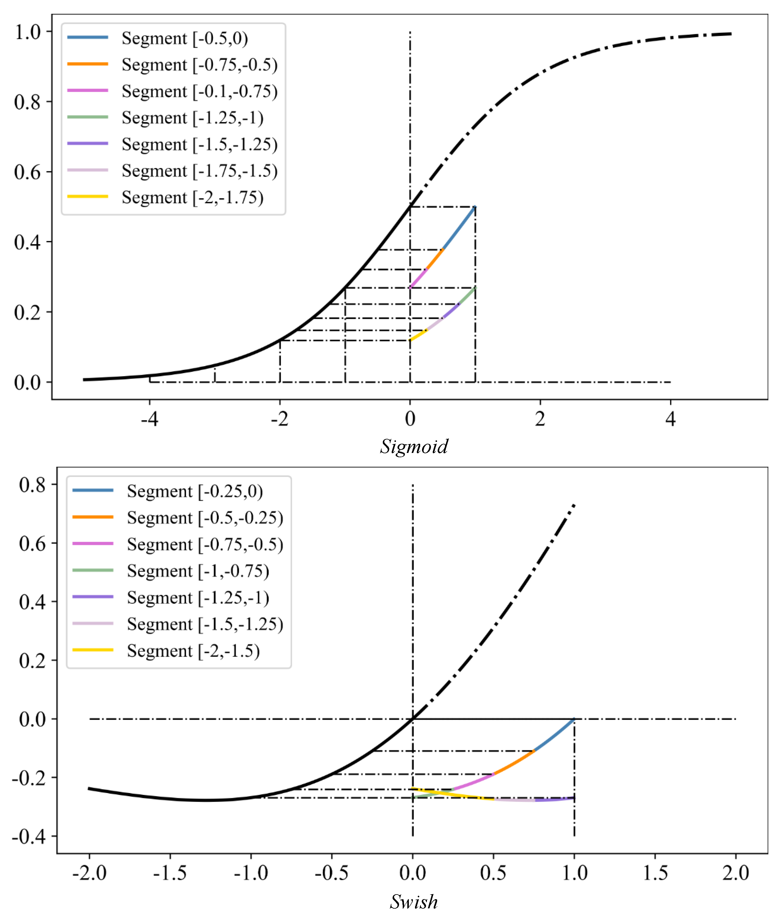
All the values in the domain of the function can be obtained according to Equation (16) by computing the value of the negative axis of the nonlinear function. After the piecewise linear approximation of the negative semi-axis nonlinear function, the slope k and intercept b of each segment of the approximate linear function can be obtained; then, the approximate value of the nonlinear function can be obtained. The segmented approximations of Swish and Sigmoid in EfficientNet are shown in Figure 9.
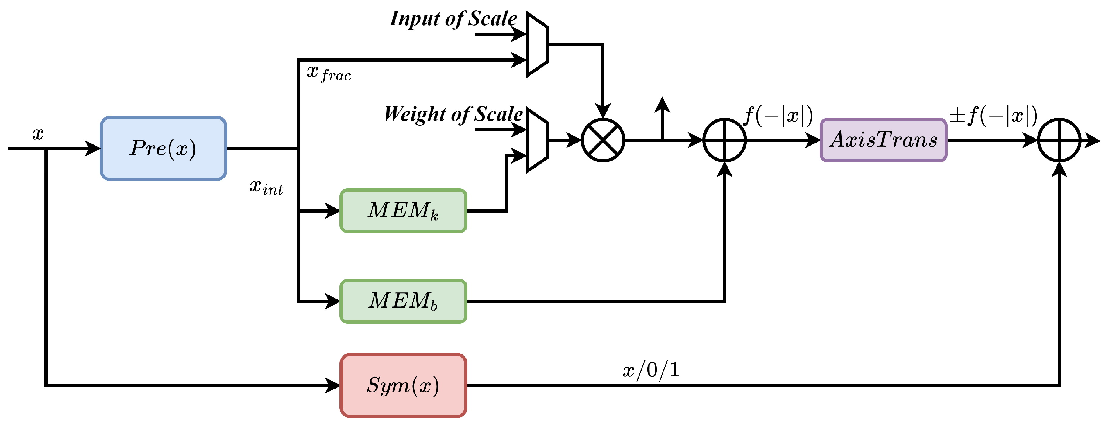
We can use the computing unit with a multiplier and adder to implement k · x + b , which is the function after the piecewise linear approximation. In addition, we notice that the hardware implementation of the scale operation also needs the multiplier. The input channel parallelisms of both the scale operation and NAF are 32. The NAF and the scale operation will not appear in the same pipeline. As a result, we can reuse the multipliers and the adders to implement both the scale operation and NAF, which are shown in Figure 10.
The P r e ( x ) module made by the XOR gate is designed to implement the | x | . The S y m ( x ) module is designed to generate 0, 1 or x. The M e m k and M e m b are made by LUT and store the slopes and intercepts of the NAF. Finally, the A x i s T r a n s module is designed to generate ± f ( | x | ) . While computing the NAF, the input ports of the multiplier are k and x. However, while computing the scale operation, the ports of multipliers are the input and weight of the scale operation.
A total of 32 groups of multipliers are set in the vector unit. The vector unit can calculate 32 groups of data, which are from 32 channels in each clock cycle. The parallelism of the input channel (ICP) is 32. The number of theoretical computation cycles of the scale operation is
T S c a l e = H · W · C 2 I C P = H · W · C 2 32
It is noted that the input size of project convolution after the scale operation is H · W · C 2 , and the convolutional kernel is 1 × 1 · C 2 · C 1 . C 2 is usually 6 times or 4 times of C 1 . In addition, both of them are usually larger than 32. The number of theoretical computation cycles of the project convolution is as follows:
T P r o = H · W · C 2 · C 1 I C P · O C P = H · W · C 2 · C 1 32 × 32 T S c a l e
By combining the scale operation with the computation of project convolution, the vector unit and the convolutional kernel are connected. The number of theoretical cycles required by the two-level computation will be reduced from T P r o + T S c a l e to T P r o . This has a very significant effect on improving the performance of the hardware accelerator.

4.4. Exchangeable-Sequence Dual-Kernel Architecture for MBCONV Module

When the accelerator performs the MBCONV module, it will flexibly configure the sequence of the computational kernel and the vector unit depending on the different operations, which are presented in Figure 11. This is another manifestation of the reconfigurability of the accelerator in this paper. Whether the vector unit performs the NAF or the scale operation, the parallelisms of both its input and output channels are 32 and equal to the channel parallelisms of the computational kernel. As a result, the computational kernel and the vector unit can form a pipeline. In particular, the output channel parallelism of 5 × 5 DWC is 16. We can store the two adjacent output data blocks on the on-chip output buffer and then send them to the vector unit.

4.5. On-Chip Input Buffer

The on-chip input buffer stores all the input activation data of a standard convolution or depthwise convolution data block. In order to make full use of the access bandwidth of the off-chip memory, the bit-width of the input buffer for STC or DWC is set to 256 bits. We can use the Ultra RAM of FPGA to form the on-chip input buffer. To broadcast the input data to the register array for DWC, we need to set five sub-memories on the on-chip buffer, which are shown in Figure 12. During the 5 × 5 DWC, the five sub-memories store 5n, 5n + 1, 5n + 2, 5n + 3 and 5n + 4 rows of data of the input feature map (IFM). The parallelism of the input channel of 5 × 5 DWC is 16, so we need to add a MUX to select the first 128 bits or last 128 bits of the input buffer. During the 3 × 3 DWC, we use the first four sub-memories to store 4n, 4n + 1, 4n + 2 and 4n + 3 rows of data of the input feature map. The parallelism of input channel of 3 × 3 DWC is 32. All data in an address of the on-chip buffer are sent to the register array in a clock cycle.
While writing data to the on-chip buffer of DWC, we need to design a counter to determine the pixel coordinate of IFM. In a data block, we first count along the channel direction, then along the column direction and finally along the row direction. To ensure that each sub-memory stores the corresponding rows of the input feature map, the sub-memory that is written in can be determined according to the row coordinate.
While writing the input data of STC, we can still use the above on-chip input buffer architecture. Four sub-memories are cascaded to store the input data according to the two most significant bits of the input address.
In particular, when the accelerator performs the scale operation of the SE module, the first four sub-memories can store the input data of the scale operation and the last one can store the weight of the scale operation.
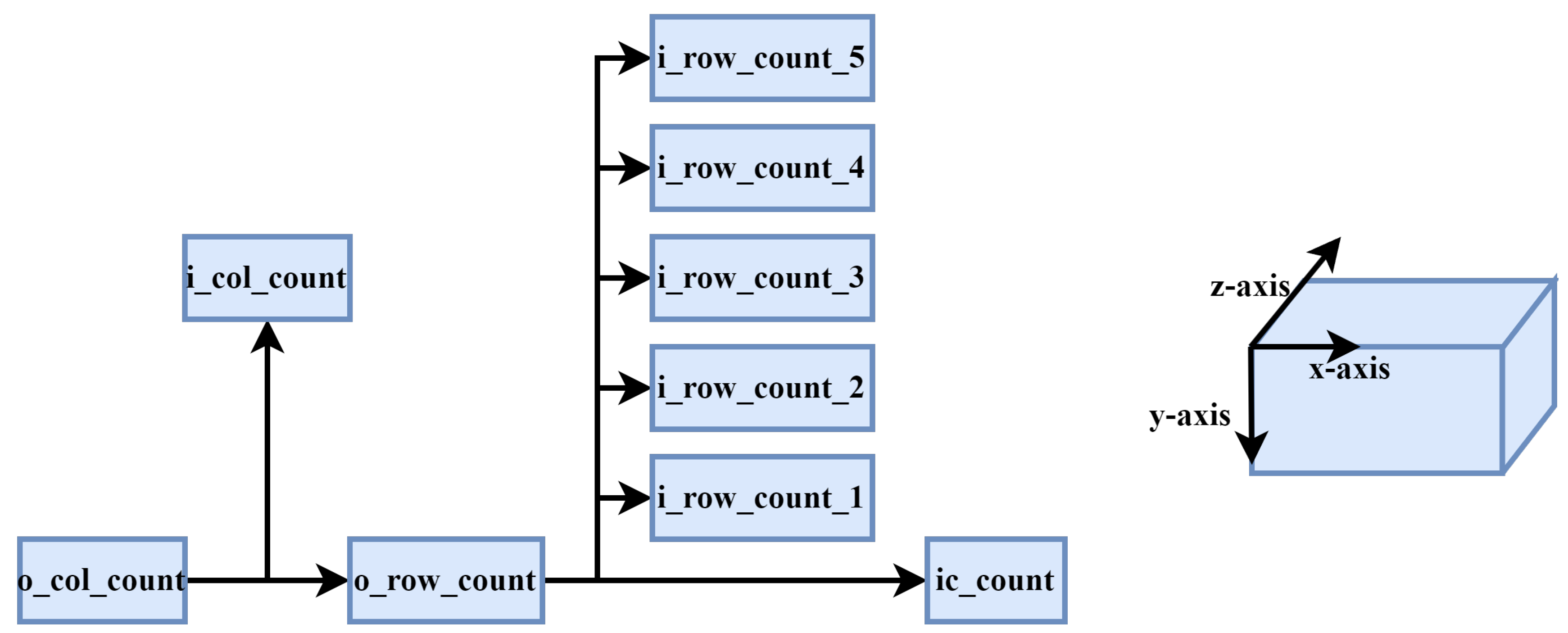
When the input data are read from the on-chip buffer to the register array, a data-read counter, which is shown in Figure 13, is designed to determine the address of pixel in the data block. Firstly, according to the column coordinate (x-axis) of the pixel on the output feature map (o_col_count), the column coordinate of the input feature map pixel (i_col_count) to be read in the on-chip buffer is determined. Then, according to the row coordinate (y-axis) of the pixel on the output feature map (o_row_count), the row coordinates of the pixels in four or five rows of IFM (i_row_count_1∼5) to be read are determined. Finally, the channel coordinate (z-axis) is generated. Four or five sub-memories will send data simultaneously to the register array during the DWC. The i_row_count corresponds to a row_addr in each sub-memory. The data-read address in each sub-memory is presented in Equation (21), where W is the width of the input feature map and IC is the numbers of input channel groups.
r d _ a d d r _ d w c = r o w _ a d d r · W · I C + c o l _ c o u n t · I C + i c _ c o u n t + s t a r t _ a d d r _ i f m
The data-read counter of STC is shown in Figure 14. Because the parallel strategy is different from that of DWC, the channel coordinate should be determined first. Then, given the two-dimensional coordinates of a pixel on the output feature map and given the two-dimensional coordinates of the corresponding weight to be calculated in this clock cycle and the stride of this convolution, the three-dimensional coordinates and the address of the input feature map pixel required in this clock cycle can be determined:
r d _ a d d r _ s t c = ( o _ r o w _ c o u n t · S + k _ r o w _ c o u n t P A D ) · W · I C + ( o _ c o l _ c o u n t · S + k _ c o l _ c o u n t P A D ) · I C + i c _ c o u n t + s t a r t _ a d d r _ i f m

5. Experimental Results

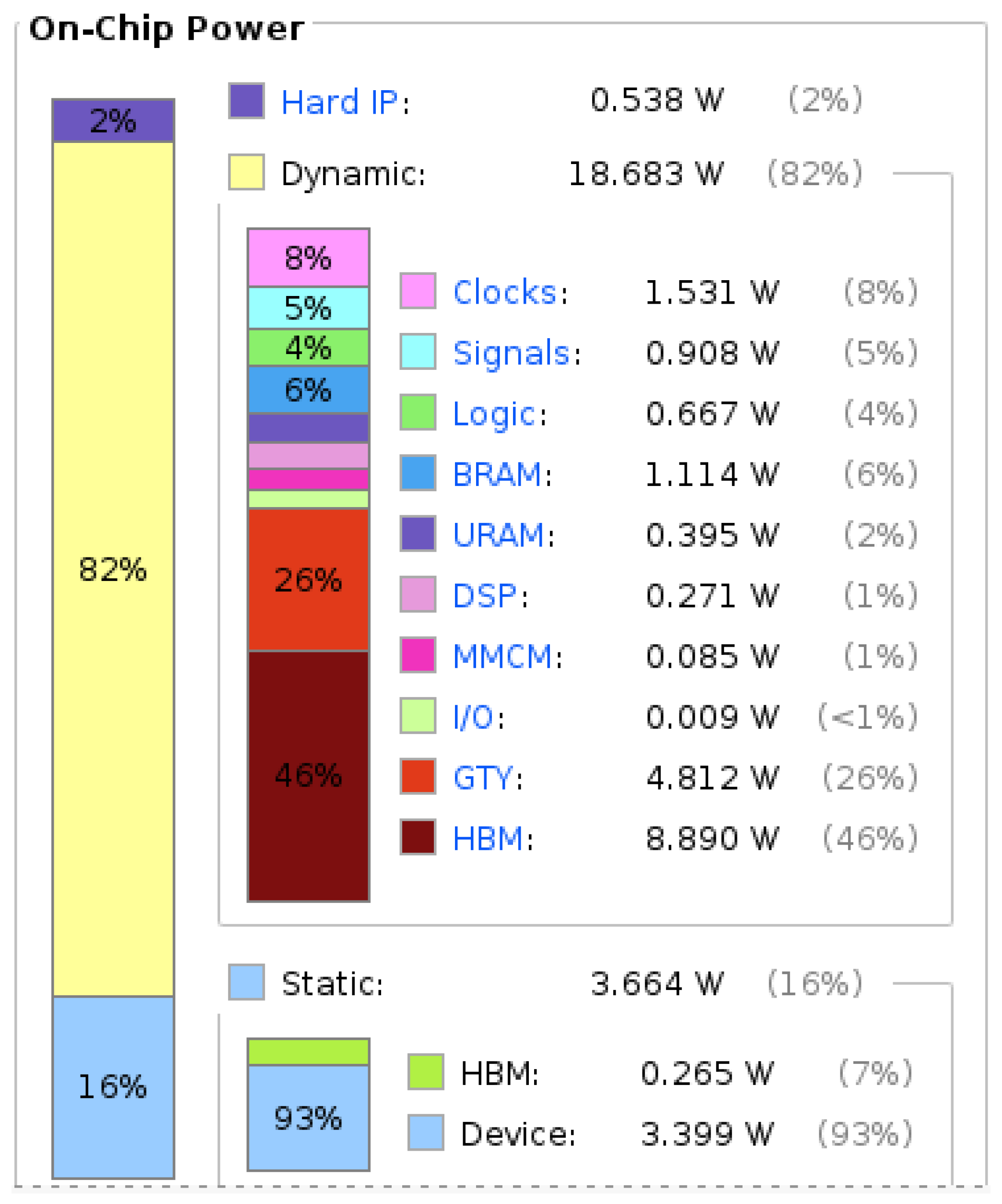
This section evaluates the performance, throughput and resource utilization of our work. Firstly, we quantize the EfficientNet-B3 in terms of INT8 precision, and the experimental result on ImageNet validation set shows that the top-1 accuracy is 80.82%, which is 0.82% lower than the accuracy of FP32 in [7]. This means that the quantization method of this paper is feasible. Next, the complete hardware accelerator is implemented on Xilinx XCVU37P by Verilog HDL. The frequency of the main system is 300 MHz, and the frequency of the DSP kernel is 600 MHz. The resource utilization of our whole hardware system is shown in Table 1, and the power estimate of our hardware system by Vivado 2021.2 is presented in Figure 15, which shows that the dynamic power of our work is 18.683 W.
We test the EfficientNet-B3 with our accelerator, and the results compared with other EfficientNet hardware accelerator are shown in Table 2. The latency of processing one image is 14.39 ms. Our hardware accelerator can achieve the performance of 69.50 FPS (frames per second) with a throughput of 255.22 GOPS (giga operations per second) in EfficientNet-B3. In [21,23,24,25], four typical EfficientNet hardware accelerators based on FPGA are presented with abundant experimental results. The hardware accelerator in [23] can only accelerate EfficientNet-B0 because of its customized pipelined architecture for each layer in EfficientNet. Compared with the latest EfficientNet-B3 accelerator [25] based on the same FPGA platform, our hardware accelerator can achieve a 1.28 times improvement in throughput. Another important metric of the FPGA accelerator is the DSP efficiency. The performance of each DSP of our work is 0.517 GOPS/DSP, which is 1.38 times that presented in [25]. There are three main reasons why the performance and DSP efficiency of our accelerator are better than LETA. Firstly, the theoretical utilization ratios of the multipliers in the computational kernel during the 3 × 3 and 5 × 5 DWC with the stride of 1 are 9/32 and 25/64, respectively, while those in LETA are only 1/8. Next, the clock cycles of our accelerator during the SE module, which are shown in Section 3.2, are at least H · W · C / 32 fewer than that of LETA. Finally, the unit for NAFs in LETA needs 64 DSP slices in total, while we only need 16 DSP slices. In addition, there are also other design details different from LETA.

6. Conclusions

A high performance hardware architecture for EfficientNet series models is proposed in this paper. Firstly, we analyze the disadvantages of the existing hardware architectures and the design space. Next, the reconfigurable computational kernel and register array are proposed to improve the performance of DWC. To accelerate the NAF and the scale operation in the SE module, the vector unit and the exchangeable-sequence dual-kernel architecture are designed. Moreover, the on-chip buffer and other key components are designed to complete the hardware accelerator. Finally, we implement the architecture based on Xilinx XCVU37P and test the performance of accelerating EfficientNet-B3. The results show that our work can achieve 1.28 times the throughput and 1.38 times the throughput/DSP compared with the EfficientNet-B3 hardware accelerator based on the same FPGA platform. This work presents higher inference performance for lightweight CNNs deployed on resource-constrained hardware platforms and makes the deployment of CNNs to mobile terminals more convenient. Moreover, this work also provides a reference for the future design of accelerators compatible with more types of CNN models.

Author Contributions

Methodology, F.A.; Validation, F.A.; Investigation, F.A.; Writing—original draft, F.A.; Writing—review & editing, F.A., L.W. and X.Z.; Supervision, L.W.; Project administration, L.W. and X.Z.; Funding acquisition, L.W. and X.Z. All authors have read and agreed to the published version of the manuscript.

Funding

This work is supported by the National Natural Science Foundation of China under grant 61971143 and the National Key R&D Program of China under grants 2022YFB4500903.

Institutional Review Board Statement

Not applicable.

Informed Consent Statement

Not applicable.

Data Availability Statement

Not applicable.

Conflicts of Interest

The authors declare no conflict of interest.

References

  1. Zhang, X.; Zhou, X.; Lin, M.; Sun, J. ShuffleNet: An extremely efficient convolutional neural network for mobile devices. In Proceedings of the 2018 IEEE/CVF Conference on Computer Vision and Pattern Recognition, Salt Lake City, UT, USA, 18–23 June 2018; pp. 6848–6856. [Google Scholar]
  2. Ma, N.; Zhang, X.; Zheng, H.T.; Sun, J. ShuffleNet v2: Practical guidelines for efficient cnn architecture design. In Proceedings of the European Conference on Computer Vision (ECCV), Munich, Germany, 8–14 September 2018; pp. 122–138. [Google Scholar]
  3. Howard, A.; Zhu, M.; Chen, B.; Kalenichenko, D.; Wang, W.; Weyand, T.; Andreetto, M.; Adam, H. MobileNets: Efficient convolutional neural networks for mobile vision applications. arXiv 2017, arXiv:1704.04861. [Google Scholar]
  4. Sandler, M.; Howard, A.; Zhu, M.; Zhmoginov, A.; Chen, L.C. MobileNetV2: Inverted residuals and linear bottlenecks. In Proceedings of the 2018 IEEE/CVF Conference on Computer Vision and Pattern Recognition, Salt Lake City, UT, USA, 18–23 June 2018; pp. 4510–4520. [Google Scholar]
  5. Howard, A.; Sandler, M.; Chu, G.; Chen, L.; Chen, B.; Tan, M. Searching for MobileNetV3. In Proceedings of the 2019 IEEE Conference on Computer Vision(ICCV), Seoul, Republic of Korea, 2–6 October 2019; pp. 1314–1324. [Google Scholar]
  6. Tan, M.; Chen, B.; Pang, R.; Vasudevan, V.; Sandler, M.; Howard, A.; Le, Q.V. MnasNet: Platform-aware neural architecture search for mobile. In Proceedings of the 2019 IEEE/CVF Conference on Computer Vision and Pattern Recognition (CVPR), Long Beach, CA, USA, 15–20 June 2019; pp. 2815–2823. [Google Scholar]
  7. Tan, M.; Le, Q. EfficientNet: Rethinking model scaling for convolutional neural Networks. In Proceedings of the 36th International Conference on Machine Learning, Long Beach, CA, USA, 9–15 June 2019; Volume 97, pp. 6105–6114. [Google Scholar]
  8. Tan, M.; Le, Q. EfficientNetV2: Smaller models and faster training. In Proceedings of the 38th International Conference on Machine Learning, Vienna, Austria, 18–24 July 2021; pp. 10096–10106. [Google Scholar]
  9. Huang, Y.; Cheng, Y.; Bapna, A.; Firat, O.; Chen, D.; Chen, M.; Lee, H.; Ngiam, J.; Le, Q.V.; Wu, Y.; et al. GPipe: Efficient training of giant neural networks using pipeline parallelism. In Proceedings of the 33rd International Conference on Neural Information Processing Systems, Vancouver, BC, Canada, 8–14 December 2019; pp. 103–112. [Google Scholar]
  10. NVIDIA Data Center Deep Learning Product Performance. 2023. Available online: https://developer.nvidia.com/deep-learning-performance-training-inference (accessed on 29 May 2023).
  11. Lammie, C.; Xiang, W.; Azghadi, M.R. Training progressively binarizing deep networks using fpgas. In Proceedings of the 2020 IEEE International Symposium on Circuits and Systems (ISCAS), Seville, Spain, 10–21 October 2020; pp. 1–5. [Google Scholar]
  12. Groom, T.; George, K. Real time fpga-based cnn training and recognition of signals. In Proceedings of the 2022 IEEE World AI IoT Congress (AIIoT), Seattle, WA, USA, 6–9 June 2022; pp. 22–26. [Google Scholar]
  13. Li, H.; Fan, X.; Jiao, L.; Cao, W.; Zhou, X.; Wang, L. A high performance FPGA-based accelerator for large-scale convolutional neural networks. In Proceedings of the 2016 26th International Conference on Field Programmable Logic and Applications (FPL), Lausanne, Switzerland, 29 August–2 September 2016; pp. 1–9. [Google Scholar]
  14. Xie, L.; Fan, X.; Cao, W.; Wang, L. High throughput cnn accelerator design based on fpga. In Proceedings of the 2018 International Conference on Field-Programmable Technology (FPT), Naha, Japan, 10–14 December 2018; pp. 274–277. [Google Scholar]
  15. Jiao, M.; Li, Y.; Dang, P.; Cao, W.; Wang, L. A high performance fpga-based accelerator design for end-to-end speaker recognition system. In Proceedings of the 2019 International Conference on Field-Programmable Technology (ICFPT), Tianjin, China, 9–13 December 2019; pp. 215–223. [Google Scholar]
  16. Wu, D.; Zhang, Y.; Jia, X.; Lu, T.; Li, T.; Sui, L.; Xie, D.; Shan, Y. A high-performance cnn processor based on fpga for MobileNets. In Proceedings of the International Conference on Field Programmable Logic and Applications (FPL), Barcelona, Spain, 8–12 September 2019; pp. 136–143. [Google Scholar]
  17. Bai, L.; Zhao, Y.; Huang, X. A cnn accelerator on fpga using depthwise separable convolution. IEEE Trans. Circuits Syst. II Express Briefs 2018, 65, 1415–1419. [Google Scholar] [CrossRef] [Green Version]
  18. Knapheide, J.; Stabernack, B.; Kuhnke, M. A high throughput MobileNetV2 fpga implementation based on a flexible architecture for depthwise separable convolution. In Proceedings of the 2020 30th International Conference on Field-Programmable Logic and Applications (FPL), Gothenburg, Sweden, 31 August–4 September 2020; pp. 277–283. [Google Scholar]
  19. Li, B.; Wang, H.; Zhang, X.; Ren, J.; Liu, L.; Sun, H.; Zheng, N. Dynamic dataflow scheduling and computation mapping techniques for efficient depthwise separable convolution acceleration. IEEE Trans. Circuits Syst. I Regul. Pap. 2021, 68, 3279–3292. [Google Scholar] [CrossRef]
  20. Xu, Y.; Wang, S.; Li, N.; Xiao, H. Design and implementation of an efficient CNN accelerator for low-cost fpgas. IEICE Electron. Express 2022, 19, 20220370. [Google Scholar] [CrossRef]
  21. Tang, Y.; Ren, H.; Zhang, Z. A reconfigurable convolutional neural networks accelerator based on fpga. In Communications and Networking. ChinaCom 2022. Lecture Notes of the Institute for Computer Sciences, Social Informatics and Telecommunications Engineering; Gao, F., Wu, J., Li, Y., Gao, H., Eds.; Springer: Cham, Switzerland, 2022; Volume 500, pp. 259–269. [Google Scholar]
  22. Xu, R.; Ma, S.; Wang, Y.; Li, D.; Qiao, Y. Heterogeneous systolic array architecture for compact cnns hardware accelerators. IEEE Trans. Parallel Distrib. Syst. 2022, 33, 2860–2871. [Google Scholar]
  23. Shivapakash, S.; Jain, H.; Hellwich, O.; Gerfers, F. A power efficiency enhancements of a multi-bit accelerator for memory prohibitive deep neural networks. IEEE Open J. Circuits Syst. 2021, 2, 156–169. [Google Scholar] [CrossRef]
  24. Nguyen, D.T.; Je, H.; Nguyen, T.N.; Ryu, S.; Lee, K.; Lee, H.-J. ShortcutFusion: From tensorflow to fpga-based accelerator with a reuse-aware memory allocation for shortcut data. IEEE Trans. Circuits Syst. I Regul. Pap. 2022, 69, 2477–2489. [Google Scholar] [CrossRef]
  25. Gao, J.; Qian, Y.; Hu, Y.; Fan, X.; Luk, W.; Cao, W.; Wang, L. LETA: A lightweight exchangeable-track accelerator for efficientNet based on fpga. In Proceedings of the International Conference on Field Programmable Technology (ICFPT), Auckland, New Zealand, 6–10 December 2021; pp. 1–9. [Google Scholar]
  26. Sifre, L. Rigid-Motion Scattering for Image Classification. Ph.D. Thesis, École Polytechnique, Paris, France, 2014. [Google Scholar]
  27. Chollet, F. Xception: Deep learning with depthwise separable convolutions. In Proceedings of the 2017 IEEE Conference on Computer Vision and Pattern Recognition (CVPR), Honolulu, HI, USA, 21–26 July 2017; pp. 1800–1807. [Google Scholar]
  28. Szegedy, C.; Vanhoucke, V.; Ioffe, S.; Shlens, J.; Wojna, Z. Rethinking the inception architecture for computer vision. In Proceedings of the 2016 IEEE Conference on Computer Vision and Pattern Recognition (CVPR), Las Vegas, NV, USA, 27–30 June 2016; pp. 2818–2826. [Google Scholar]
  29. Fu, Y.; Wu, E.; Sirasao, A.; Attia, S.; Khan, K.; Witting, R. Deep Learning with INT8 Optimization on Xilinx Devices. Available online: https://www.xilinx.com/support/documentation/whitepapers/wp486-deep-learning-int8.pdf (accessed on 24 April 2017).
  30. Williams, S.; Waterman, A.; Patterson, D.; Witting, R. Roofline: An insightful visual performance model for multicore architectures. Commun. ACM 2009, 52, 65–76. [Google Scholar] [CrossRef] [Green Version]
  31. Feng, X.; Li, Y.; Qian, Y.; Gao, J.; Cao, W.; Wang, L. A high-precision flexible symmetry-aware architecture for element-wise activation functions. In Proceedings of the 2021 International Conference on Field-Programmable Technology (ICFPT), Auckland, New Zealand, 6–10 December 2021; pp. 1–4. [Google Scholar]
Figure 1. MBCONV with SE module in EfficientNet.
Electronics 12 02847 g001
Figure 2. Separated engine architecture and unified engine architecture [19].
Electronics 12 02847 g002
Figure 3. The ratio of the standard convolution and the depthwise convolution of the first 14 operation pairs in EfficientNet-B3.
Electronics 12 02847 g003
Figure 4. Three parallel strategies commonly used for depthwise convolution.
Electronics 12 02847 g004
Figure 5. The system architecture of our work.
Electronics 12 02847 g005
Figure 6. Pipeline architecture of the hardware accelerator.
Electronics 12 02847 g006
Figure 7. The computing process of 5 × 5 DWC.
Electronics 12 02847 g007
Figure 8. Splitting method and architecture of the register array.
Electronics 12 02847 g008
Figure 9. The segmented approximations of Swish and Sigmoid functions.
Electronics 12 02847 g009
Figure 10. The hardware architecture for the scale operation and NAF.
Electronics 12 02847 g010
Figure 11. The exchangeable-sequence dual-kernel architecture for MBCONV module.
Electronics 12 02847 g011
Figure 12. The On-chip Buffer for DWC.
Electronics 12 02847 g012
Figure 13. The data-read counter for DWC.
Electronics 12 02847 g013
Figure 14. The data-read counter for STC.
Electronics 12 02847 g014
Figure 15. The power estimate of our hardware accelerator.
Electronics 12 02847 g015
Table 1. The resource usage of our hardware system.
ResourceUtilizationAvailableUtilization (%)
LUT138,5191,303,68010.6
FF197,7992,607,3607.6
BRAM220.5 *201610.9
URAM409604.2
DSP49490245.5
* BRAM Sizes are unified to 36 Kb.
Table 2. Performance comparisons with other accelerators based on FPGA.
Paper [23]Paper [21]Paper [24]Paper [25]Our Work
PlatformXilinx XCVU440Xilinx ZC706Xilinx KCU1500Xilinx XCVU37PXilinx XCVU37P
Process20 nm28 nm20 nm16 nm16 nm
Frequency180 MHz100 MHz200 MHz300 MHz300 MHz
DSP1008 *N/A2240534494
ModelEfficientNet-B0EfficientNet-lite0EfficientNet-B1EfficientNet-B3EfficientNet-B3
PrecisionINT16INT8INT8INT8INT8
Input Size224 × 224 × 3224 × 224 × 3256 × 256 × 3300 × 300 × 3300 × 300 × 3
MAC Operations (B)0.780.771.383.673.67
Latency (ms)N/A5.14.6918.414.39
Frame Rate (FPS)231.2196.1213.254.369.50
Frame Rate/DSP (FPS/DSP)0.229N/A0.09510.1020.141
Throughput (GOPS)180.3150.6317.1199.6255.22
Throughput/DSP (GOPS/DSP)0.179N/A0.1420.3740.517
* DSP numbers of the accelerator using INT16 quantization method are unified to INT8 for comparisons.
Disclaimer/Publisher’s Note: The statements, opinions and data contained in all publications are solely those of the individual author(s) and contributor(s) and not of MDPI and/or the editor(s). MDPI and/or the editor(s) disclaim responsibility for any injury to people or property resulting from any ideas, methods, instructions or products referred to in the content.