

Near-Field Coupling Effect Analysis of SMD Inductor Using 3D-EM Model
 , ,
, , 
Abstract
1. Introduction
2. Equivalent Circuit Model of SMD Inductor from Impedance Measurement
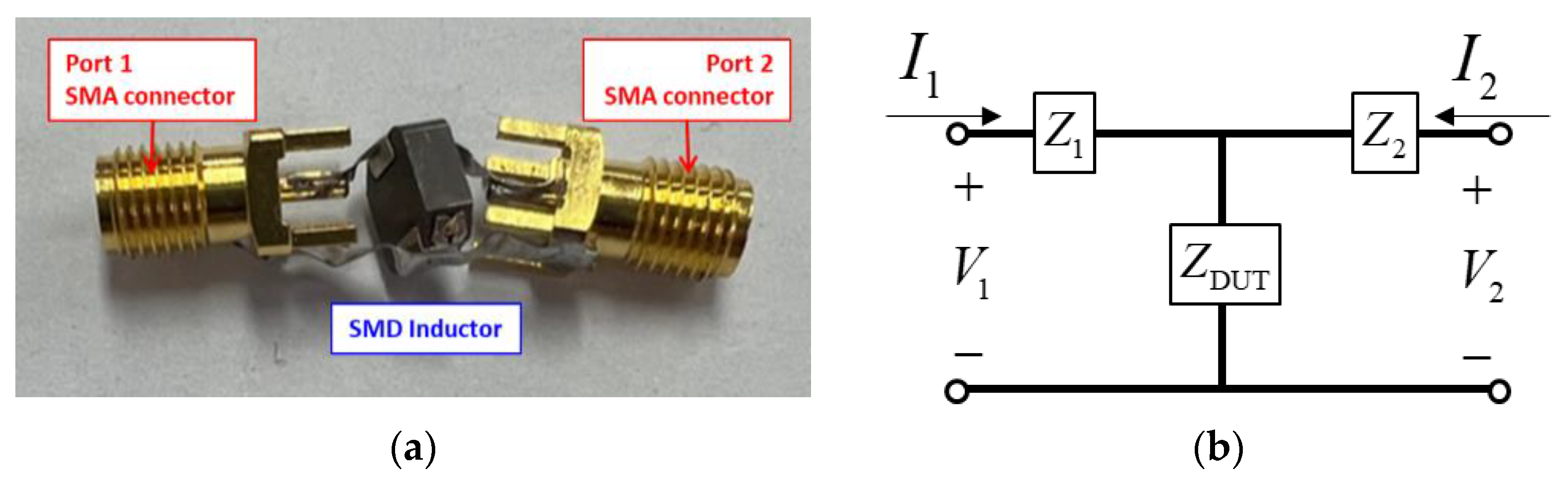
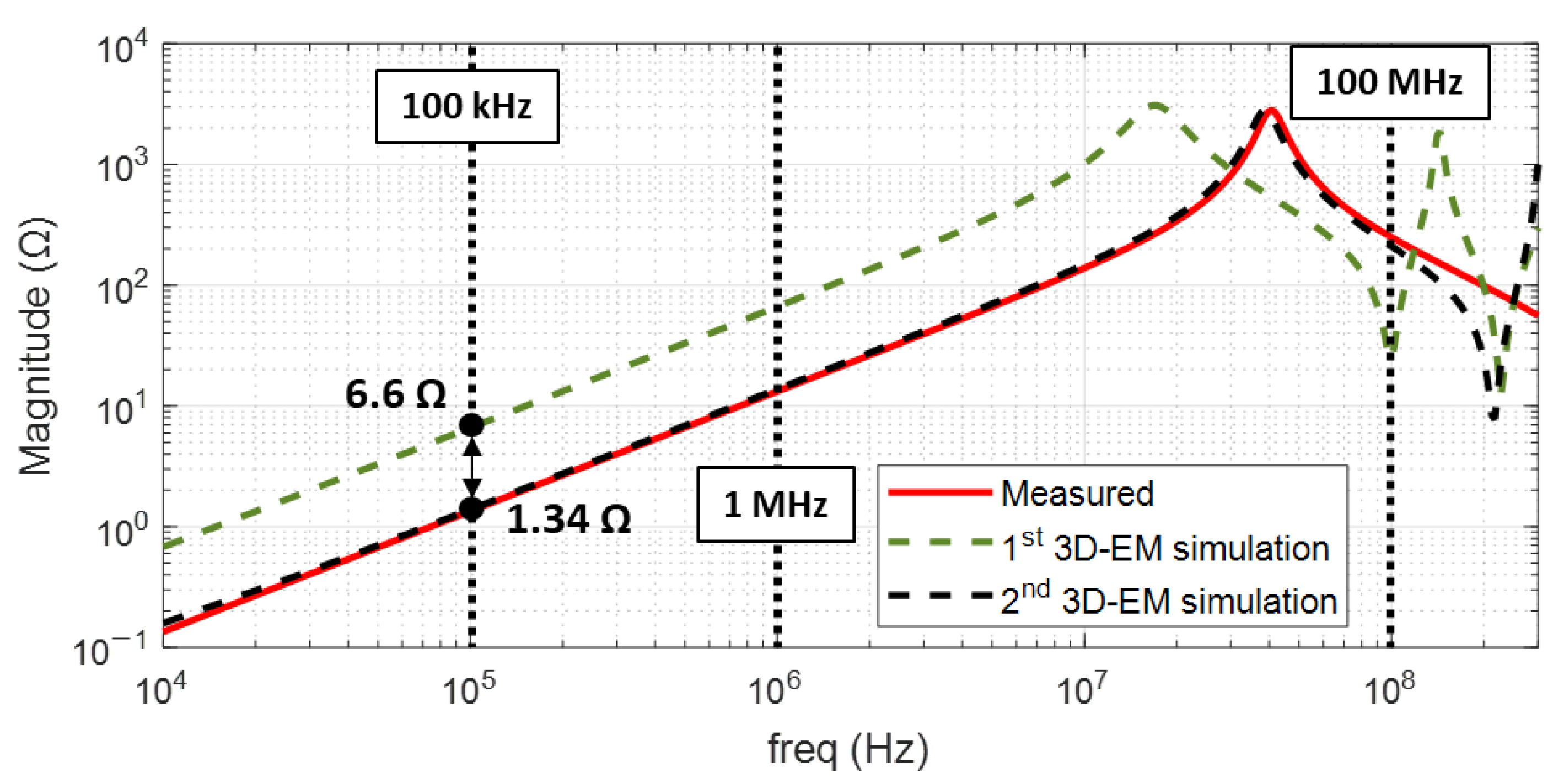
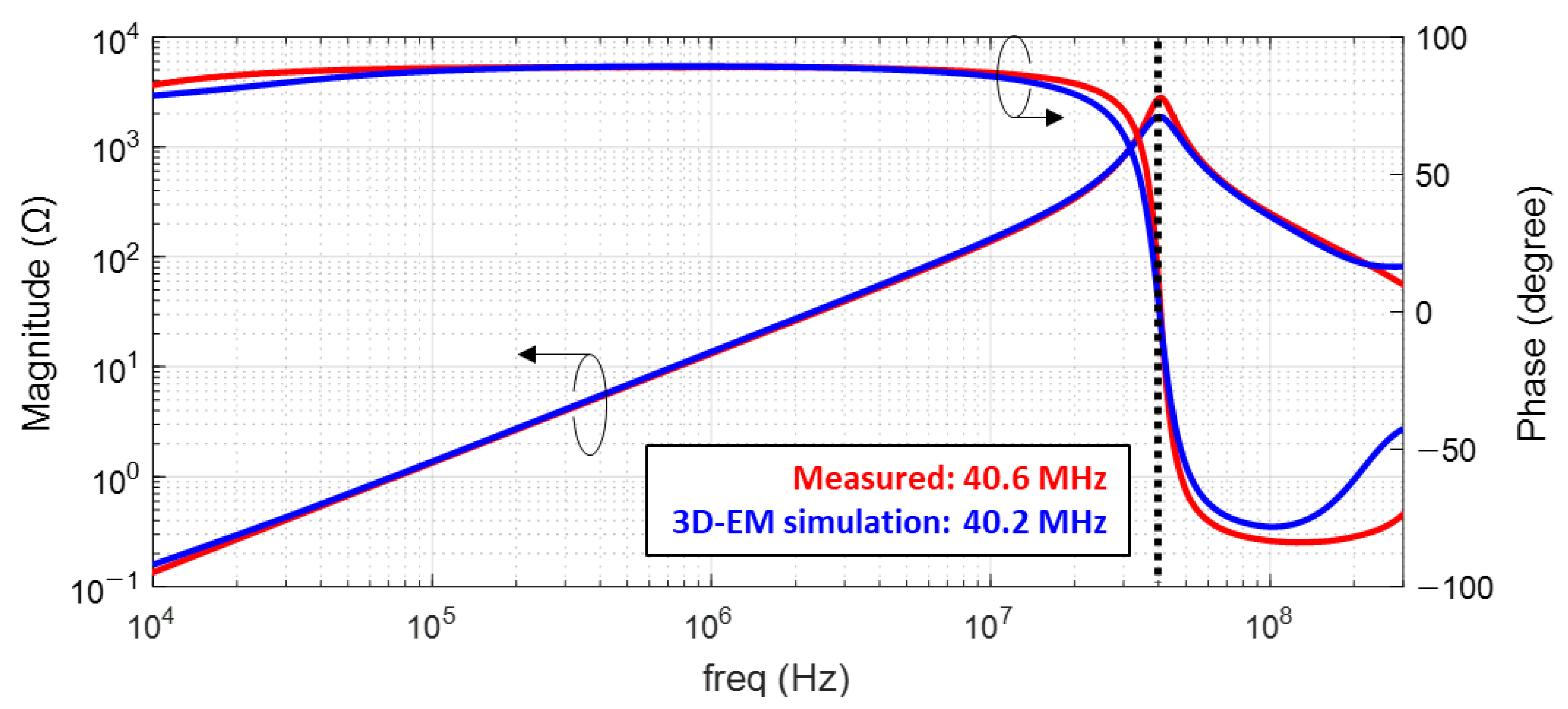
2.1. Impedance Measurement of Wire-Wound Inductor
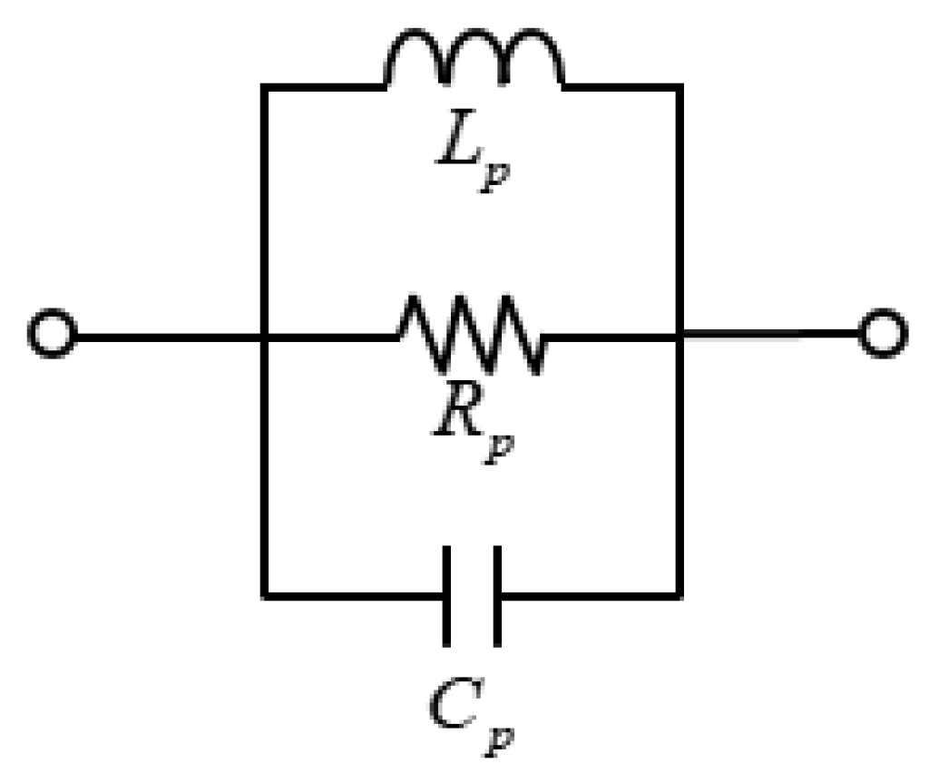
2.2. Equivalent Circuit Analysis
3. 3D-EM Model of SMD Inductor
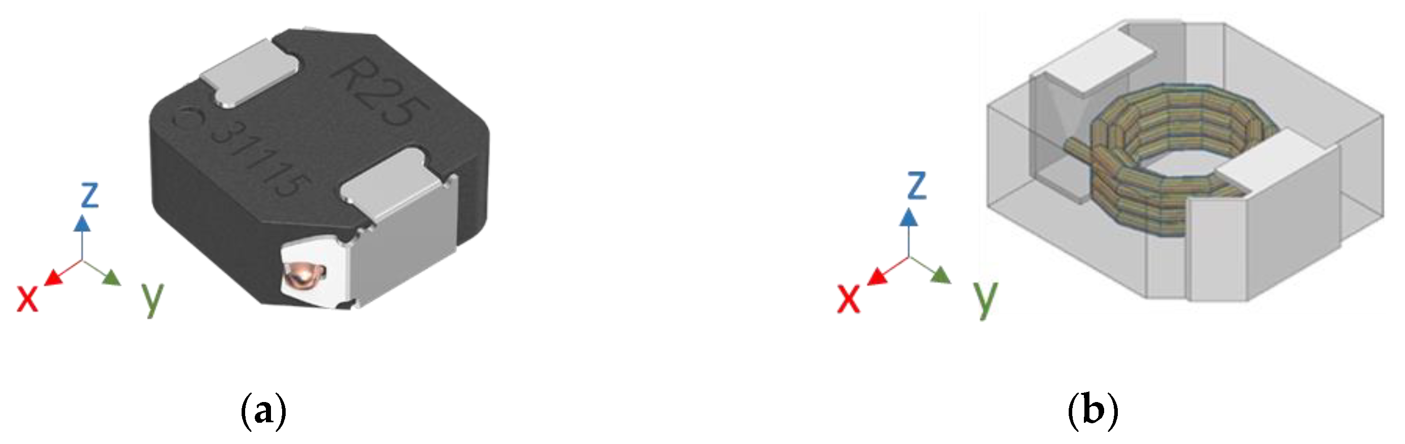
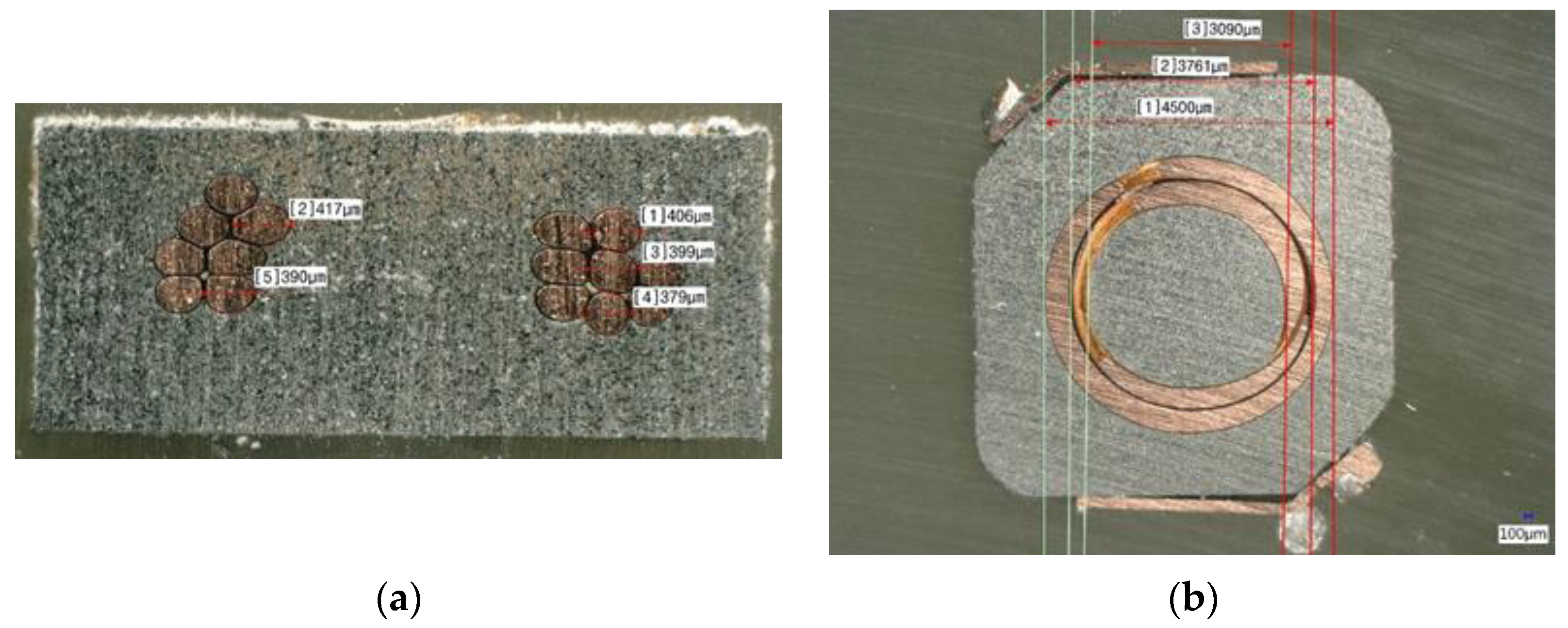
3.1. Inner Structure Acquisition to Produce 3D-EM Model
3.2. Permeability Estimation in the Low Frequency Region
3.3. The Damped Harmonic Oscillator
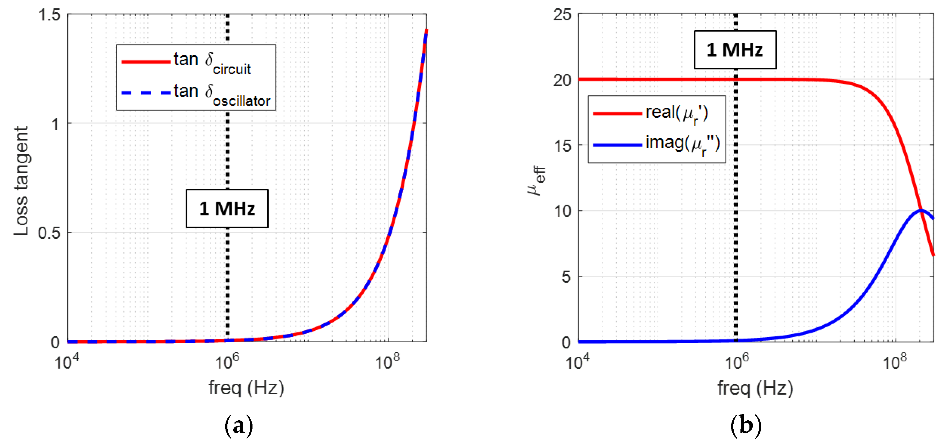
- The complex permeability formula from damped harmonic oscillator model is set as in (11), and the three unknown variables need to be determined.
- Another loss tangent from the impedance of circuit model in (13) should be calculated, and the two loss tangents are compared to be equal, for finding the three unknowns using optimization algorithm.
3.4. Optimization Process
- (1)
- (2)
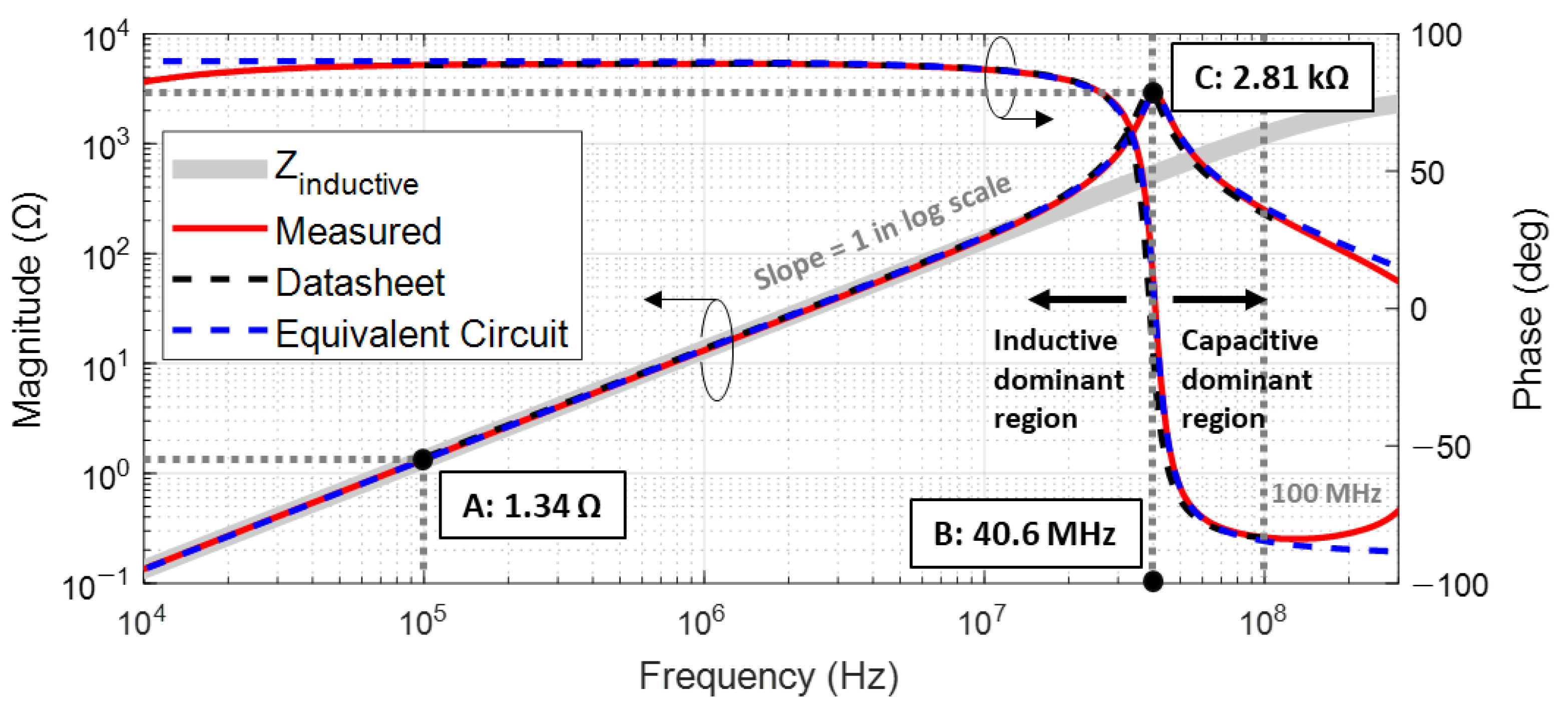
- Loss tangent, , came from experiment, which means that includes the loss in the air as well as the loss in the magnetic material. However, noting that loss tangent in the air is null, it is reasonable to say that mainly represents the loss tangent of magnetic material in the SMD inductor. Then, we compared the two loss tangents in (12) and (13) for the estimation of . So, the increase of could be mainly due to the core loss in the magnetic material above 1 MHz in Figure 7b.
- (3)
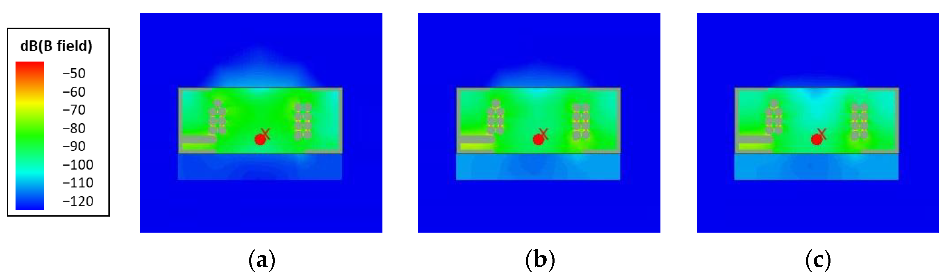
- Since were derived by the comparison of two loss tangents, not by comparison of the data, it would be instructive to check the magnetic field distribution around the SMD inductor. Figure 8 shows cross sectional view of the magnetic field distribution around SMD inductor at 100, 200 and 300 MHz, respectively, using 3D-EM model. One can see that most of the magnetic fields is restricted inside the core material of the inductor for the three cases.
4. Tuning of Other Electrical Properties
4.1. Permittivity Tuning
4.2. Conductivity Tuning
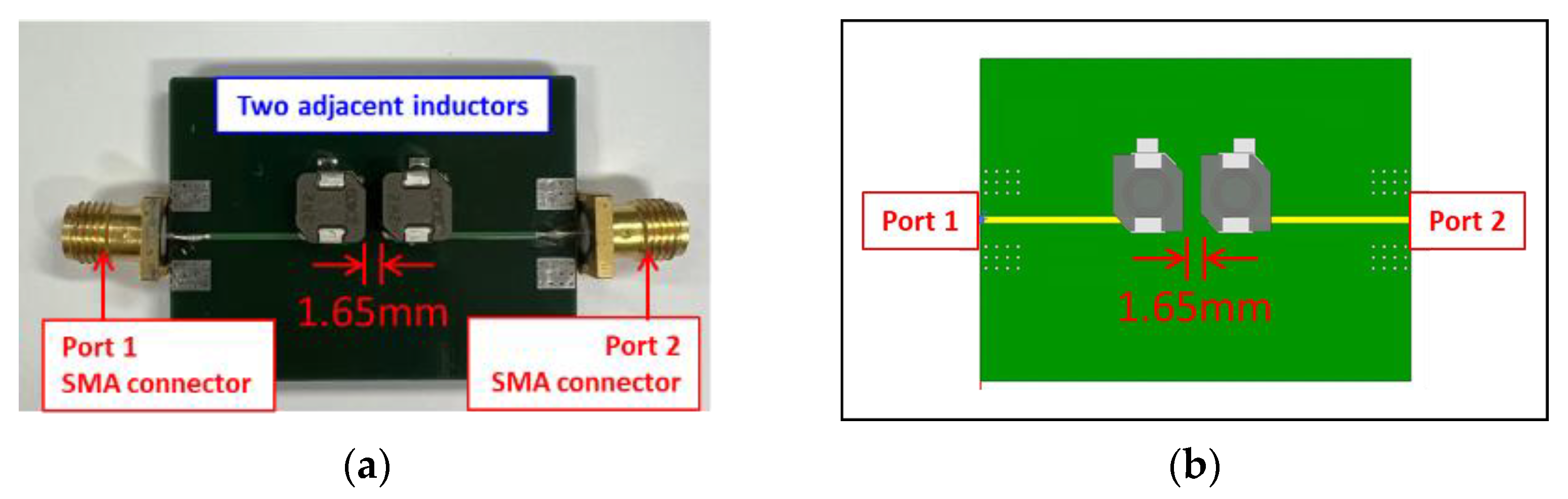
5. Near Field Coupling Analysis
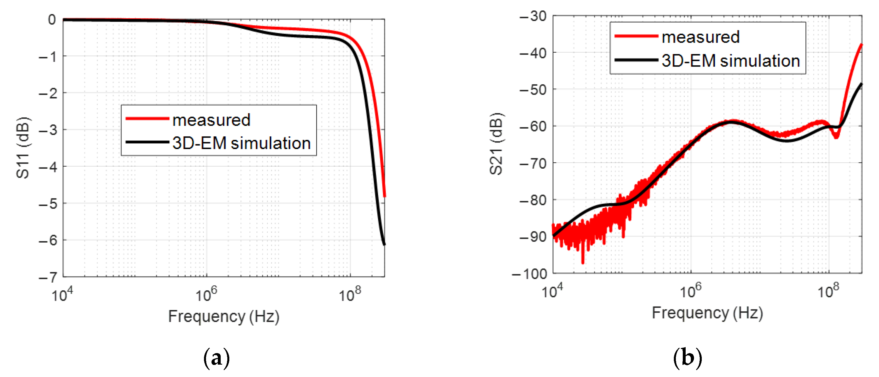
5.1. Validation of SMD Inductor 3D-EM Model
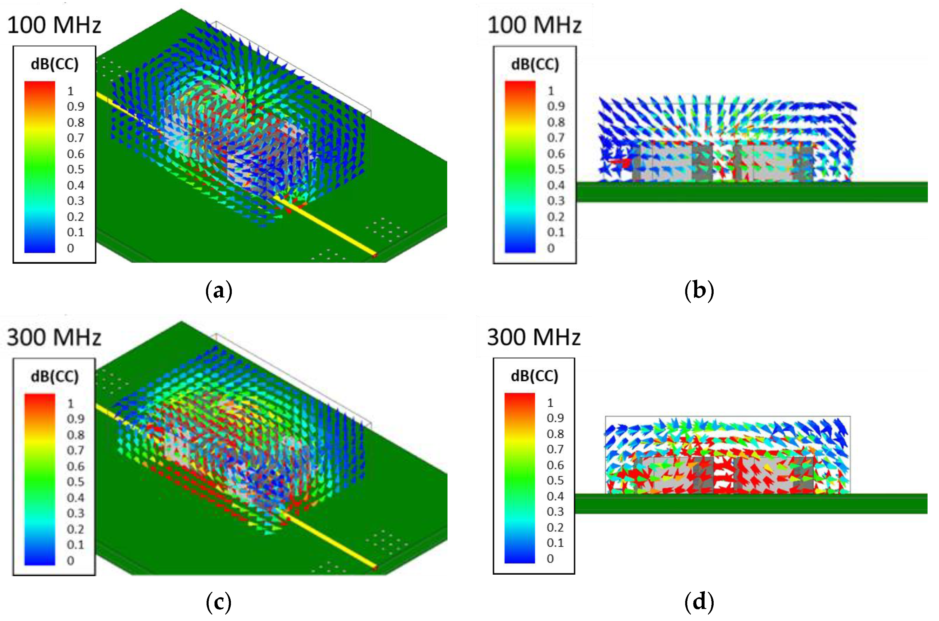
5.2. Coupling Path Visualization
6. Conclusions
- (1)
- The inductance formula of SMD inductor is not available in an analytic form, so we measured experimental impedance, which was used to develop a circuit model. So the loss tangent of the magnetic material of SMD inductor was effectively defined using the circuit parameters in the developed circuit model.
- (2)
- The damped harmonic oscillator model, a well-known model that satisfies the Kramers-Kronig relationship, was introduced for comparison with the circuit parameters in terms of loss tangent.
- (3)
- The two loss tangents, one from the circuit model and the other from damped harmonic oscillator model were compared to extract the complex permeability of SMD magnetic material.
- (4)
- The P2SO optimization method, which was developed based on the PSO algorithm, to avoid a local minimum and the complex permeability was efficiently applied to find the optimized permeability values, which turned out to be valid.
Author Contributions
Funding
Data Availability Statement
Conflicts of Interest
References
- Asmanis, A.; Stepins, D.; Asmanis, G.; Ribickis, L. 3D Modelling and Analysis of Parasitic Couplings between Surface-Mount Components of EMI Filters. In Proceedings of the 2018 IEEE International Symposium on Electromagnetic Compatibility and 2018 IEEE Asia-Pacific Symposium on Electromagnetic Compatibility (EMC/APEMC), Suntec City, Singapore, 14–18 May 2018; pp. 496–501. [Google Scholar] [CrossRef]
- TDK Product Center. Available online: https://product.tdk.com/en/techlibrary/productoverview/inductors_spm.html (accessed on 4 January 2023).
- Liu, J.P.; Willard, M.; Tang, W.; Brück, E.; de Boer, F.; Liu, E.; de Visser, A. Metallic Magnetic Materials. In Handbook of Magnetism and Magnetic Materials; Springer: Berlin/Heidelberg, Germany, 2021; pp. 693–808. [Google Scholar]
- Willard, M.; Laughlin, D.T.; McHenry, M.E.; Thoma, D.J.; Sickafus, K.E.; Cross, J.O.; Harris, V.G. Structure and Magnetic Properties of (Fe0.5Co0.5)88Zr7B4Cu1 Nanocrystalline Alloys. J. Appl. Phys. 1999, 84, 6773–6777. [Google Scholar] [CrossRef]
- Zhang, B.; Wang, S. Analysis and Reduction of the Near Magnetic Field Radiation from Magnetic Inductors. In Proceedings of the 2017 IEEE Applied Power Electronics Conference and Exposition (APEC), Tampa, FL, USA, 26–30 March 2017; pp. 2494–2501. [Google Scholar] [CrossRef]
- Chu, Y.; Wang, S.; Zhang, N.; Fu, D. A Common Mode Inductor with External Magnetic Field Immunity, Low-Magnetic Field Emission, and High-Differential Mode Inductance. IEEE Trans. Power Electron. 2015, 30, 6684–6694. [Google Scholar] [CrossRef]
- Kondo, Y.; Izumichi, M.; Shimakura, K.; Wada, O. Modeling of Bulk Current Injection Setup for Automotive Immunity Test Using Electromagnetic Analysis. IEICE Trans. Commun. 2015, E98-B, 1212–1219. [Google Scholar] [CrossRef]
- Joo, J.; Kwak, S.I.; Kwon, J.H.; Song, E. Simulation-Based System-Level Conducted Susceptibility Testing Method and Application to the Evaluation of Conducted-Noise Filters. Electronics 2019, 8, 908. [Google Scholar] [CrossRef]
- Liu, X.; Grassi, F.; Spadacini, G.; Pignari, S.A.; Trotti, F.; Mora, N.; Hirschi, W. Behavioral Modeling of Complex Magnetic Permeability with High-Order Debye Model and Equivalent Circuits. IEEE Trans. Electromagn. Compat. 2021, 63, 730–738. [Google Scholar] [CrossRef]
- Cuellar, C.; Tan, W.; Margueron, X.; Benabou, A.; Idir, N. Measurement Method of the Complex Magnetic Permeability of Ferrites in High Frequency. In Proceedings of the 2012 IEEE International Instrumentation and Measurement Technology Conference Proceedings, Graz, Austria, 13–16 May 2012; pp. 63–68. [Google Scholar] [CrossRef]
- Shenhui, J.; Quanxing, J. An Alternative Method to Determine the Initial Permeability of Ferrite Core Using Network Analyzer. IEEE Trans. Electromagn. Compat. 2005, 47, 651–657. [Google Scholar] [CrossRef]
- Cuellar, C.; Idir, N.; Benabou, A. High-Frequency Behavioral Ring Core Inductor Model. IEEE Trans. Power Electron. 2016, 31, 3763–3772. [Google Scholar] [CrossRef]
- Kącki, M.; Ryłko, M.S.; Hayes, J.G.; Sullivan, C.R. Measurement Methods for High-Frequency Characterizations of Permeability, Permittivity, and Core Loss of Mn-Zn Ferrite Cores. Electronics 2022, 37, 15152–15162. [Google Scholar] [CrossRef]
- Topping, C.V.; Blundell, S.J. AC Susceptibility as a Probe of Low-Frequency Magnetic Dynamics. J. Phys. Condens. Mater. 2019, 31, 013001. [Google Scholar] [CrossRef] [PubMed]
- Xie, C.; Zhou, L.; Ding, S.; Liu, R.; Zheng, S. Experimental and numerical investigation on self-propulsion performance of polar merchant ship in brash ice channel. Ocean. Eng. 2023, 269, 113424. [Google Scholar] [CrossRef]
- TDK Product Center. Available online: https://product.tdk.com/en/search/inductor/inductor/smd/info?part_no=SPM6530T-2R2M-HZ (accessed on 4 January 2023).
- Ponomarenko, N.; Solovjova, T.; Grizans, J. The Use of Kramers-Kronig Relations for Verification of Quality of Ferrite Magnetic Spectra. Electr. Control Commun. Eng. 2016, 9, 30–35. [Google Scholar] [CrossRef]
- TDK. EPCOS Databook. Ferrite and Accessories. 2013. Available online: https://www.tdk-electronics.tdk.com/download/519704/069c210d0363d7-b4682d9ff22c2ba503/ferrites-and-accessories-db-130501.pdf (accessed on 4 January 2023).
- Kang, S.; Kim, S. Particle 2-Swarm Optimization for Robust Search. J. Inf. Oper. Manag. 2008, 18, 1–10. (In Korean) [Google Scholar]
- Kim, K. PCB-Type EMI Filter Design Methodology Combined with Large Busbar Using P2SO Algorithm. Ph.D. Dissertation, Sungkyunkwan University, Seoul, Republic of Korea, 2022. (In Korean). [Google Scholar]
- Zhou, X.; Cai, X.; Zhang, H.; Zhang, Z.; Jin, T.; Chen, H.; Deng, W. Multi-strategy competitive-cooperative co-evolutionary algorithm and its application. Inf. Sci. 2023, 635, 328–344. [Google Scholar] [CrossRef]
- Kennedy, J.; Eberhart, R. Particle Swarm Optimization. In Proceedings of the ICNN’95—International Conference on Neural Networks, Perth, WA, Australia, 27 November–1 December 1995; Volume 4, pp. 1942–1948. [Google Scholar] [CrossRef]
- Holland, J.H. Adaptation in Natural and Artificial Systems; University of Michigan Press: Ann Arbor, MI, USA, 1975. [Google Scholar]
- Zhong, Y.; Song, W.; Kim, C.; Hwang, C. Coupling Path Visualization and Its Application in Preventing Electromagnetic Interference. IEEE Trans. Electromagn. Compat. 2020, 62, 1485–1492. [Google Scholar] [CrossRef]
- Rumsey, V.H. Reaction Concept in Electromagnetic Theory. Phys. Rev. 1954, 94, 1483–1491. [Google Scholar] [CrossRef]
- Balanis, C.A. Advanced Engineering Electromagnetics; Wiley: New York, NY, USA, 1989. [Google Scholar]


Disclaimer/Publisher’s Note: The statements, opinions and data contained in all publications are solely those of the individual author(s) and contributor(s) and not of MDPI and/or the editor(s). MDPI and/or the editor(s) disclaim responsibility for any injury to people or property resulting from any ideas, methods, instructions or products referred to in the content. |
© 2023 by the authors. Licensee MDPI, Basel, Switzerland. This article is an open access article distributed under the terms and conditions of the Creative Commons Attribution (CC BY) license (https://creativecommons.org/licenses/by/4.0/).
Share and Cite
Choi, G.R.; Kim, H.; Hong, Y.; Hwang, J.; Kim, E.; Nah, W. Near-Field Coupling Effect Analysis of SMD Inductor Using 3D-EM Model. Electronics 2023, 12, 2845. https://doi.org/10.3390/electronics12132845
Choi GR, Kim H, Hong Y, Hwang J, Kim E, Nah W. Near-Field Coupling Effect Analysis of SMD Inductor Using 3D-EM Model. Electronics. 2023; 12(13):2845. https://doi.org/10.3390/electronics12132845
Chicago/Turabian StyleChoi, Gyeong Ryun, HyongJoo Kim, Yonggi Hong, Joosung Hwang, Euihyuk Kim, and Wansoo Nah. 2023. "Near-Field Coupling Effect Analysis of SMD Inductor Using 3D-EM Model" Electronics 12, no. 13: 2845. https://doi.org/10.3390/electronics12132845
APA StyleChoi, G. R., Kim, H., Hong, Y., Hwang, J., Kim, E., & Nah, W. (2023). Near-Field Coupling Effect Analysis of SMD Inductor Using 3D-EM Model. Electronics, 12(13), 2845. https://doi.org/10.3390/electronics12132845