Article

Analytical Approach to Improve the Performance of a Fully Integrated Class-F Power Amplifier with 0.13 µm BiCMOS Technology Using Drain–Bulk Capacitor Modulation

by
Smail Traiche
1,2,*,†,
Mohamed Trabelsi
1,†,
Ali Bououden
2 and
Mustapha C. E. Yagoub
3
1
Ecole Nationale Polytechnique, El-Harrach, Algiers 16200, Algeria
2
Center for Development of Advanced Technologies (CDTA), Baba Hassen, Algiers 16081, Algeria
3
School of Electrical Engineering and Computer Science, University of Ottawa, Ontario, ON K1N 61N, Canada
*
Author to whom correspondence should be addressed.
These authors contributed equally to this work.
Electronics 2023, 12(13), 2784; https://doi.org/10.3390/electronics12132784
Submission received: 30 April 2023 / Revised: 26 May 2023 / Accepted: 8 June 2023 / Published: 23 June 2023
(This article belongs to the Special Issue Advanced Design of RF/Microwave Circuit)

Abstract

:
This article reports a novel technique based on drain–bulk capacitor modulation to improve the performance design of a class-F power amplifier (PA) used in low-power transceivers based on the I-Q amplitude modulation technique considering linearity–efficiency–miniaturization trade-offs. This idea is carried out by implementing a tuned capacitor in parallel with a cascode transistor on the output of the power stage to enhance the shape of the voltage–current amplitudes of the class-F PA by creating a new harmonic current component. Simulated results were obtained for the power back-off region of the proposed configuration, with an output power, power gain and power-added efficiency of 8 dBm (+ 5 dBm) B , 19 dB (+ 5 dB) B and 45% (+ 5% to 10%) B , respectively. In addition, post-layout simulations revealed a similar level of output power, a power gain of a 20 dB and a 28% power-added efficiency for an added capacitance equal to 1.3 pF. Class-F PA is implemented on a 732 × 605   μ m 2 chip’s surface. ( B : indicates the improved values in the power back-off region).

1. Introduction

The ever-increasing development of radiofrequency and microwave systems, which are widely used in wireless devices such as mobile smartphones, tablets, and laptops, has highlighted the crucial need for efficient power consumption systems [1]. Power amplifiers (PAs) are generally the most dissipative bloc in front-end transceivers, due to their significant gain in power and the strong current drawn by the load. Therefore, several works have aimed to reduce the transceiver power consumption by mainly targeting the power amplifier [2,3]. The design of PAs dedicated for use in mobile systems, essentially those using submicron technologies such as CMOS [4] and BiCMOS, is mainly based on a tradeoff between linearity and efficiency, as adopted for the design of amplitude-modulation transceivers. Power amplifiers can be divided into two main groups. The first, the linear group, is characterized by a very good linearity but a weak efficiency. In contrast, the second one, the switching non-linear group, is defined by a very good efficiency coupled with poor linearity.
Although research on the latter mainly focuses on improving the PA’s performance based on output network tunability, several works have been reported on tuning the output impedance to enhance both the efficiency and output power while minimizing distortions [5,6]. In some cases, a feedback branch constituting series inductance and capacitance was inserted to couple the residue of the RF signal drain, leading to an enhanced in-hand linearity and slightly improving the efficiency of a 3G LTE class-F CMOS power amplifier [7]. By merging the output filter and the output-matching network of a class-F power amplifier, the authors of [8,9] endeavored to reduce the passive components losses, thus obtaining a higher efficiency and higher output power levels. In paper [10], a differential continuous class-F PA with four different output networks based on choke-inductance, transformer-balun, and the second harmonic branch was proposed to enhance the efficiency and output power levels in the desired frequency band. In the same context of shaping drain voltage and current waveforms [11,12,13], second, third or multiple harmonics are kept at GaN, FET and GaAs pHEMT transistor drain levels to make the fundamental and corresponding harmonic components a function of the conduction angle. In [14], the bandwidth was broadened over one octave by using resistive impedance at the second harmonic, resulting in a relative decrease in efficiency while maintaining the same level of output power in a GaN HEMT Class-F power amplifier. Other works have focused on the modulation of the output network by tuning the harmonic resonant and/or the output matching network capacitances, as reported in [15,16,17]. This tunability is ensured by on-chip transformers with parallel variable capacitances, by inserting a high Q varactor to enhance the overall efficiency or by implementing an output matching network based on transmission lines for harmonic control. In this case, the output power is increased by employing a stacked transistor topology and a combiner based on the transformer topology. In [18], a bulk 65 nm CMOS power amplifier based on a Doherty architecture was reported. The amplifier was reconfigured by digitally controlled principal-peaking amplifiers and a power splitter–combiner, providing the option to address the antenna mismatch and enhance the efficiency in the deep back-off region, while respecting the efficiency–linearity trade-off. Mixed non-linear class power amplifiers have also been the subject of research aiming to improve their power efficiency by adding a quarter wave transmission line to the output network, as in [19]. The reported bipolar-based class-FE switching power amplifier was designed using an analytical approach that demonstrated the effects of connecting a parallel transmission line to the collector capacitor on the voltage–current waveforms. Such a structure combines the class-F operating mode with class-E switching conditions, resulting in a high efficiency being achieved at higher frequencies.
Moreover, other reported works have shown the impact of drain waveform shaping on reducing the dissipative power. Mansour, in [20], designed a multi-mode linear (class-AB)/switching (class-F) double-stage cascode PA with an output network constituting of a second–third harmonics network and a series matching network. This structure was mainly employed to drive both sinusoidal and square input signal forms. Dong, in [21], employed a coupled-inductor-based harmonic impedance modulator in order to terminate second and third harmonic load impedances appropriately for an inverse class-F PA operating in mm-wave. Tsai, in [22], proposed a differential power cell class-F PA with a thin oxide MOS g m and a thick oxide HVMOS cascode dedicated to GSM/EDGE/TD-SCDMA/TD-LTE transmitters, where tunability was ensured by transformers and capacitors, designed to maximize the gain and improve linearity .
This paper is organized as follows: In Section 2, the structure of the proposed class-F power amplifier, with an output capacitance in parallel with the cascode stage, will be theoretically analyzed. Then, in Section 3, the class-F power amplifier will be designed and thoroughly compared to existing designs. The conclusion of this work will be outlined in Section 4. Mostly, this work consists of using the analytical approach reinforced by Post-Layout simulations to demonstrate the impact of an additional capacitor on the PA’s performances.

2. Proposed Class-F PA Structure

2.1. Theoretical Study of Class-F Power Amplifiers

In order to reduce the transistor losses and increase the efficiency, the adopted class-F power amplifier is theoretically defined with an infinite number of harmonic resonators at its output to shape the voltage waveform and make it closer to a squared signal [3]. In fact, the class-F structure consists of a capacitor C o u t in parallel with the cascode transistor stage, as depicted in Figure 1 [3]. This capacitor takes values between [0.1 pF and 1.3 pF] to ensure the PAs’ stability and to avoid huge frequency shifts in the S parameters of the active stage. Note that the bulk sides of all transistors are connected to the ground, except transistor P1, which is connected to V D D . In addition, a third harmonic resonator is set to combine the third harmonic component with the fundamental one to shape the drain voltage waveform. At the output level, a fundamental resonator is included to bring the fundamental current and voltage components into the load at a central frequency f 0 of 2.45 GHz, between [2.4 GHz and 2.5 GHz], for a narrow bandwidth of 100 MHz.
In Figure 2, the parasitic elements of the two transistors M 1 and M 2 are considered. The output network is composed of an impedance transformation, a third harmonic resonator, a fundamental resonator and a variable capacitor C o u t associated with the parasitic capacitors, C g d 1 , C g d 2 the gate-drain capacitances, and C d b 1 , C d b 2 the drain-bulk capacitances. The four capacitors are gathered to make an equivalent capacitor C e q , defined as
C e q = C d b 2 + C g d 2 ( C o u t ) C d b 1 + C g d 2 + C o u t
The effect of this capacitor on the output impedance Z n e t will determine the behavior of the power amplifier. Transistors P 1 and M 3 act as a current mirror that determines the DC current of the power stage by fixing the current gain between the current mirror stage and the power stage. Transistors P 1 and M 3 act as a voltage divider that determines the gate voltage of transistor M 1 .

2.2. The Added Output Capacitance’s Effect on the Input Impedance and Stability of the Designed PA

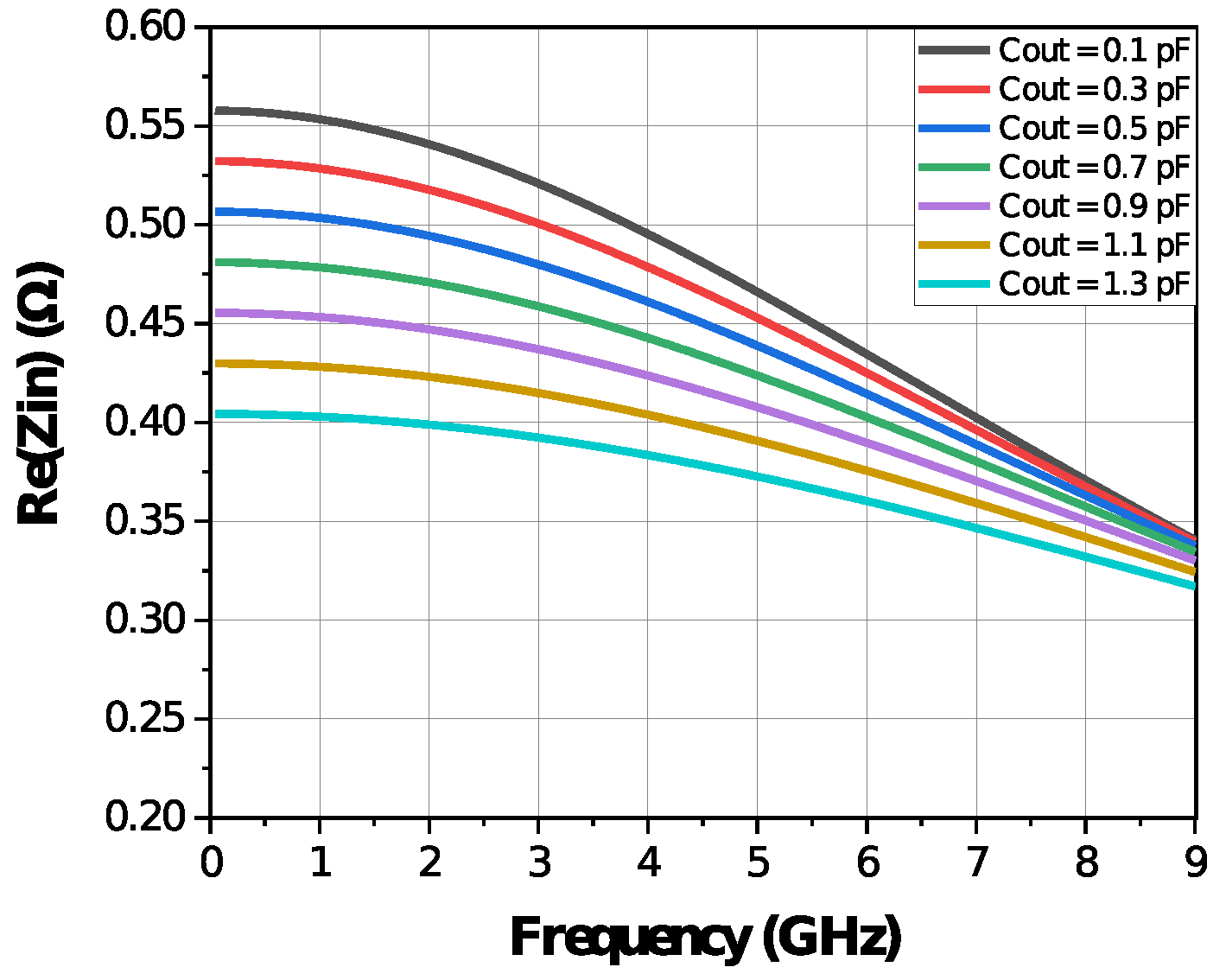
Figure 3 shows the real part of an input impedance Z i n of a class-F PA, illustrated as follows in expression (2)
Z i n = 1 j ω 1 C g s 1 ( C g d 1 A C B + D )
A = g m 1 j C g d 1 ω
B = 1 r d s 1 + j C d b 1 + C g d 1 + C g s 2 ω
C = g m 2 + j C g d 2 ω
D = 1 r d s 2 + j C o u t + C g d 2 ω
where the parasitic capacitances C g s 1 , C g s 2 and transconductances g m 1 , g m 2 are the gate- source capacitances and transconductances of transistors M 1 and M 2 , respectively.
A, B, C and D are represented in Expressions (2)–(6), respectively. The real part of the impedance Z i n is strictly positive for different values of C o u t ; therefore, the designed class-F PA is unconditionally stable.

2.3. Impact of the Added Output Capacitance on the Output Network Impedance

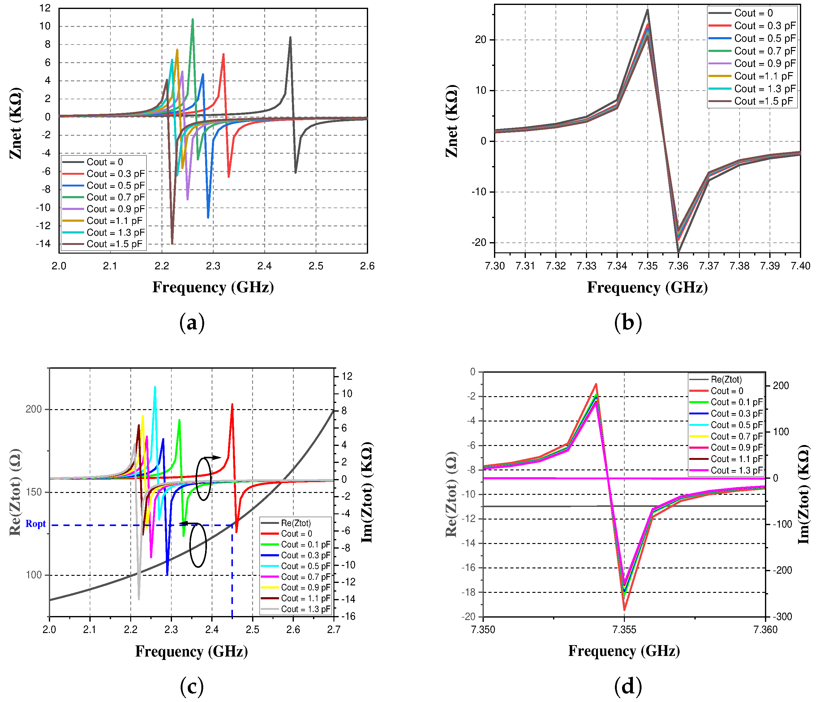
As shown in Figure 2, the output network is composed of the harmonic network and the output matching circuit. The harmonic network, which is mainly formed by combining the proposed output capacitance C o u t with the harmonic circuit ( C 3 , L 3 ) and the fundamental frequency resonator ( C 0 , L 0 ), is responsible for keeping the harmonic components at the drain level, as shown in Figure 2. This structure is expected to guard the voltage third harmonic and current second harmonic components to shape the drain’s voltage and current components, respectively, as well as possible. Analytically, the input impedance of the harmonic network Z n e t can be expressed as a function of the capacitance C e q = f( C o u t ), as illustrated in Expression (7).
Z n e t = j L 0 + L 3 1 L 0 L 3 C 0 + C 3 L 0 + L 3 ω 2 ω 1 C 3 L 3 ω 2 1 C 0 L 0 + C 3 C e q L 0 + L 3 C 3 + C e q ω 2
In this expression, the denominator highlights the existence of two poles corresponding to the third harmonic of the drain voltage and the fundamental component of the drain voltage (which is mainly dependent on C e q ). The nominator exhibits two zeros corresponding to ω = 0 and ω = 2 ω 0 , with the latter being dependent on C 0 , C 3 , L 0 and L 3 . Therefore, the impedance Z n e t is responsible for guarding the harmonic components at the drain level.
The magnitude of the purely imaginary output network impedance | Z n e t | must be investigated as a function of C e q = f( C o u t ) to evaluate its impact on the drain voltage–current waveforms’ shaping and, hence, on the class-F P A performances. As shown in Figure 2, Z T represents the impedance between the optimal resistance of the active stage and the load R L , which is equal to the characteristic impedance of the antenna (50 Ω ). Applying Thevenin’s theorem, Z T is given by (8),
Z T = j L T C T L T ω 1 C T ω
where L T and C T are the elements of the output matching network. The total impedance Z t o t of the overall output network seen from the active stage, which is a function of the optimal resistance R o p t of the power stage, can be expressed as:
Z t o t = R o p t / / Z n e t / / Z T = R o p t / / j X n e t / / j X T
Z t o t = R o p t X n e t X T R o p t 2 X n e t + X T 2 + X n e t 2 X T 2 X T X n e t + j R o p t X n e t + X T
where X n e t , X T represent the reactance parts of impedances Z n e t and Z T , respectively.
The voltage gain G v = V L V i n , which is the ratio of the load voltage V L to the input voltage V i n , is defined by expression (11). The voltage gain is at the heart of all performance evaluations.
G v = Z 0 R L R L + j L T ω Z 0 + Z 3 1 + j Z 0 C T ω A C B + D
where A, B, C and D are mentioned above and Z 0 and Z 3 are the impedances of the fundamental and third harmonic circuits, respectively,
Z 0 = j L 0 C 0 L 0 ω 0 1 C 0 ω 0
Z 3 = j L 3 C 3 L 3 ω 1 C 3 ω
As shown in Figure 4, upon observing the impact of the proposed output capacitor C o u t on varying fundamental components in Figure 4a, a third harmonic component is clearly demonstrated in Figure 4b of Z n e t . This permits the impedance value versus frequency to be shifted, as well as tuning its reactive part. Furthermore, the capacitance C o u t allows for the total output impedance Z t o t to be tuned, slightly reinforcing the magnitude of the third harmonic voltage component. Its real part is equal to the optimal resistance R o p t = 130 Ω at the operating frequency f 0 . In addition, prior calculations have demonstrated that the second harmonic current is dependent on the nominator of Z n e t . As a result, the two kept components, i.e., the third harmonic voltage and the second harmonic current, will be merged with the fundamental voltage/current components, respectively. Therefore, designing a class-F PA by modulating the drain–bulk capacitance by varying C o u t looks to be a quite promising and original approach to better shaping the drain waveforms. Although the conventional concept of a class-F PA design leads to an improved drain efficiency and power, in addition to power compression and saturated power points, the proposed approach should improve the complete performance in the entire power back-off region, while maintaining a good linearity.

2.4. Added Output Capacitance’s Impact on Parameters at the Drain Level

Before exploiting the above-mentioned approach, let us set some well-known key design parameters. To establish a relationship between the drain efficiency η and the drain power dissipation of transistor M 2 , we must begin by illustrating the relation between modules of instantaneous drain dissipative power and instantaneous drain voltage–current, expressed as
p D t = 1 2 π 0 2 π v D S ( t ) i D ( t ) d θ = V D D I D V m I m 2
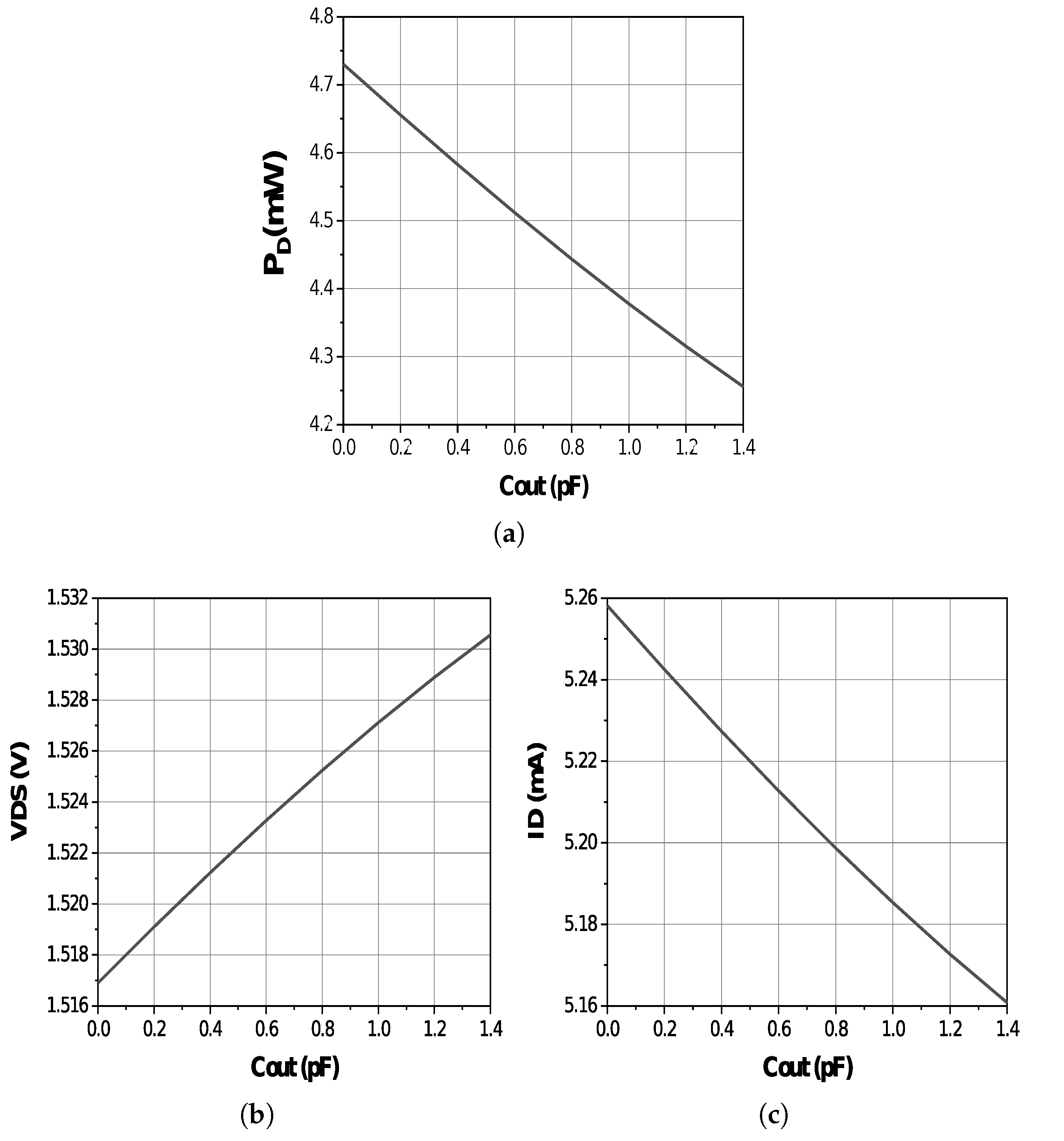
where V D S ( t ) and i D ( t ) are the instantaneous drain voltage and drain current, respectively. Furthermore, V m and i m are fundamental voltage–current components, respectively. Figure 5a represents the amplitude of dissipating power, which exhibits a remarkable decrease with the evolution of C o u t . Expression (14) leads to
P D = P D C 1 η
where P D C is the power supplying the PA. Notice that the drain efficiency η has a direct relationship with C o u t through the voltage gain G v , as will be demonstrated below in (22)–(28). Thus, from (14) and (15), the maximal drain voltage magnitude has the following expression
V D S   max = P D C 1 η I D   max
where V D S m a x and I D m a x are the maximal values of drain voltage and current waveforms, respectively, which are directly deduced from the Fourier transforms of the time-domain drain voltage–current waveforms, expressed as
v D S = V D D + V m cos cos θ 0 V m 3 cos cos 3 θ 0
i D = I D I m cos cos ( θ 0 ) + I m 2 cos ( 2 θ 0 )
where V m and V m 3 are the amplitudes of the fundamental and third voltage components, respectively, whereas I m and I m 2 are the amplitudes of the fundamental and second harmonic current components, respectively. Furthermore, the DC components of v D S and i D are depicted in Figure 5b and Figure 5c, respectively, where the former increases and latter decreases with the evolution of C o u t . To obtain the optimal resistance R o p t of the active stage, we applied the maximally flat drain voltage waveform reported in [3] by calculating the maximal amplitudes at pulsation θ 0 = π . The DC component of the current for the class-F PA is then
I D = 9 V D D V D S   min 4 π R o p t
where V D D is the supplied voltage and V D S m i n is the knee voltage. Then, from (17) to (19), we have
V m 2 9 8 V D D R o p t I D V m + 9 R o p t 8 P D C 1 η I D V D D = 0
As can be noted, this equation is a second-order equation with two solutions, which are
V m ± = 1 2 9 8 V D D R o p t I D ± ( 9 8 V D D R o p t I D ) 2 9 R o p t 8 ( P D C ( 1 η ) I D V D D )
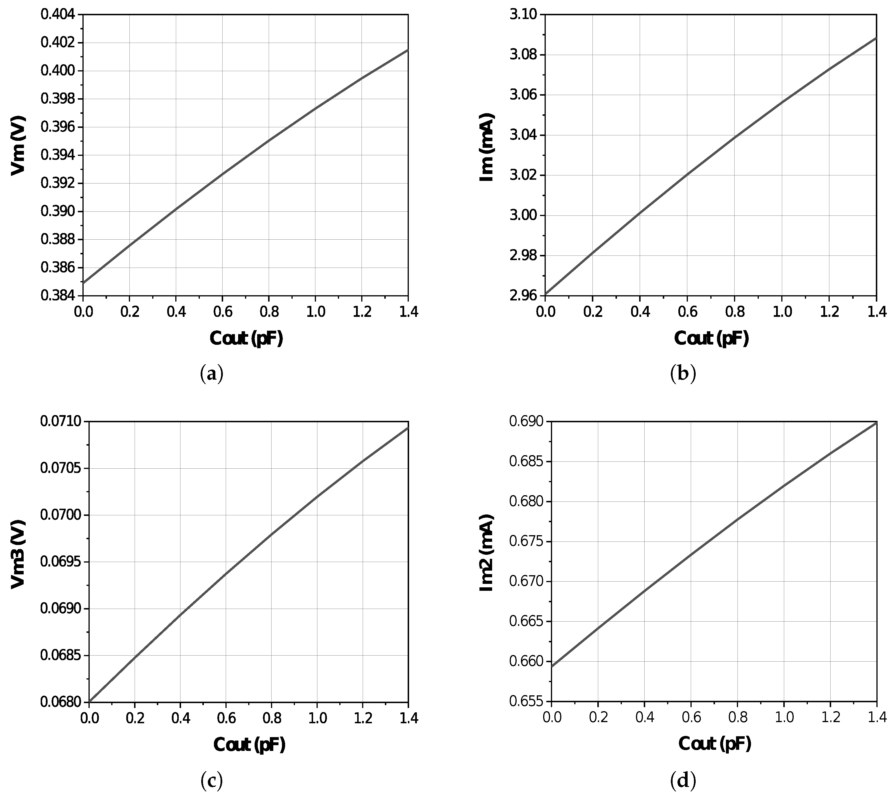
Let V m 3 = V m 5.66 , I m = V m R o p t and I m 2 = I m 4.23 be the harmonic component relationships deduced beforehand using the power stage spectra extracted from simulations for C o u t = 0 . They were recalculated through V m ± values following Formula (21) for C o u t 0 . According to Figure 6, the fundamental and harmonic forms of drain voltage–current could evolve with a capacitance C o u t to a good shaping, thus enlarging the overlap between drain waveforms and weakening the dissipate power P D . More accurately, a third harmonic voltage is merged with a fundamental one and the second harmonic current is merged with the fundamental one at the drain level, where the voltage and current are out-phased at 180 . Thus, the added capacitance reduces the current and reinforces the voltage in the first half-period and acts inversely in the second half-period, provoking a drain dissipate power reduction. This operation impacts the PAs’ output parameters, as will be shown in the next section

2.5. The Added Output Capacitor’s Impact on Class-F Power Amplifier Performance

As a result of the added output capacitance C o u t having a considerable impact on the output network impedance and the drain signal waveforms, the whole performance of the designed class-F power amplifier are affected, the parameters of which are summarized in Table 1. Therefore, the intrinsic parasitic components of the two transistors refer to the BSIM 4 model, which simulates the 0.13   μ m BiCMOS process.
To investigate the effect of C o u t on the amplifier, let us begin by expressing its input power P i n and load power P L
P L = 1 2 V L 2 R e Z L P i n P i n
P i n = 1 2 V i n 2 R e Z i n
where Z i n and Z L are the input and load impedances, respectively. From the above expressions, we can obtain
P L = R e Z i n R e Z L V L 2 V i n 2 P i n
For the active stage, we can deduce the power gain
G P = R e Z i n R e Z L G v 2
Thus, the drain efficiency, η , and the power-added efficiency, PAE, are
η = R e Z i n R e Z L G v 2 P i n P D C
P A E = R e Z i n R e Z L G v 2 P i n 2 P D C 1 P i n 1 P L
The voltage gain in these equations constitutes a key design parameter from which all the other PA performance metrics can be deduced using the data shown in Table 1. After a theoretical development, I L can be expressed as
I L = 2 G p P i n R L 1 2
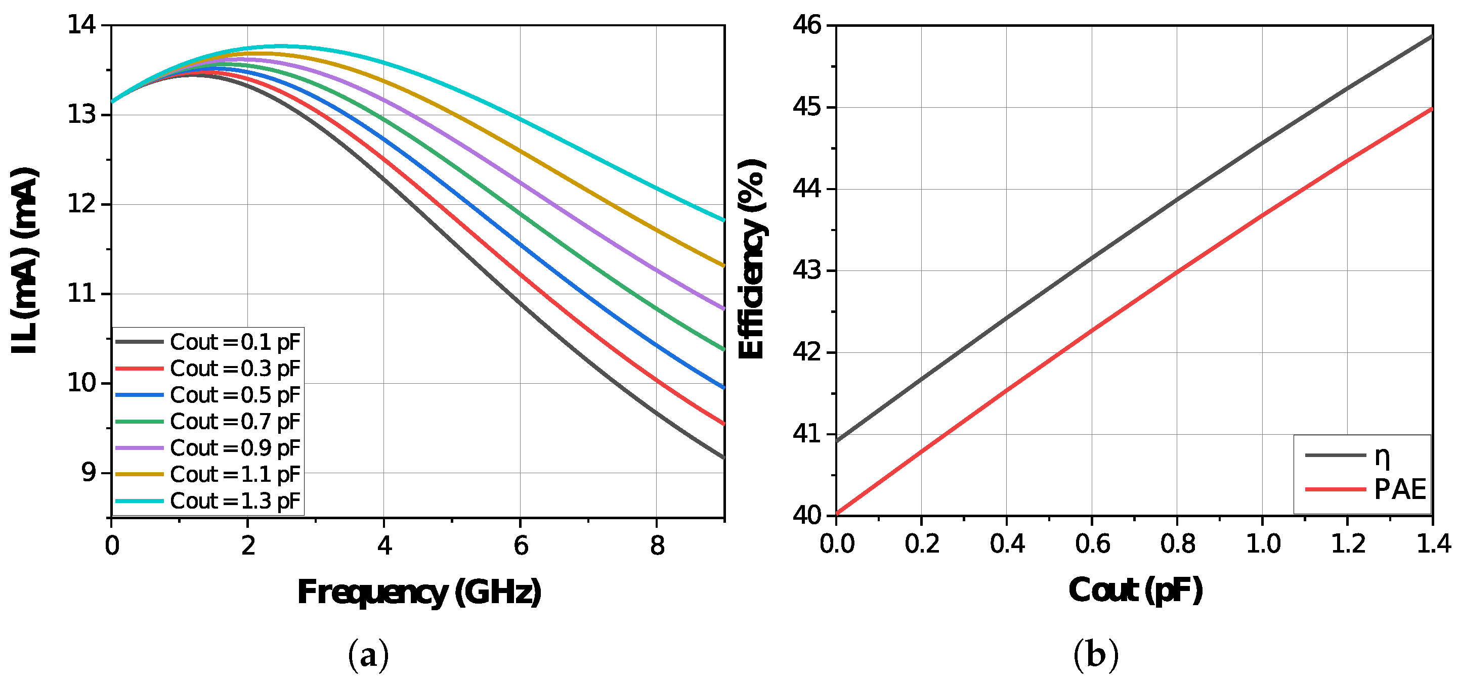
Analytically, two important parameters are sufficiently demonstrated to illustrate the effect of C o u t on the PA’s performance improvement. In fact, Figure 7a illustrates the output current experienced to the load with frequency evolution for different values of C o u t , following the expression (28). This figure demonstrates a substantial consequent increase in the load current and output power. Furthermore, C o u t serves to broaden the PAs bandwidth, as this capacitance permits an overall quality factor degradation. Similarly, the drain efficiency η and the added power efficiency PAE as functions of capacitance C o u t (Expressions (26) and (27)), are shown in Figure 7b. These two performances are clearly improved by 5%, from 40% to 45% for the first one, and from 41% to 46% for the second.

3. Class-F Power Amplifier Design with Lossy Components

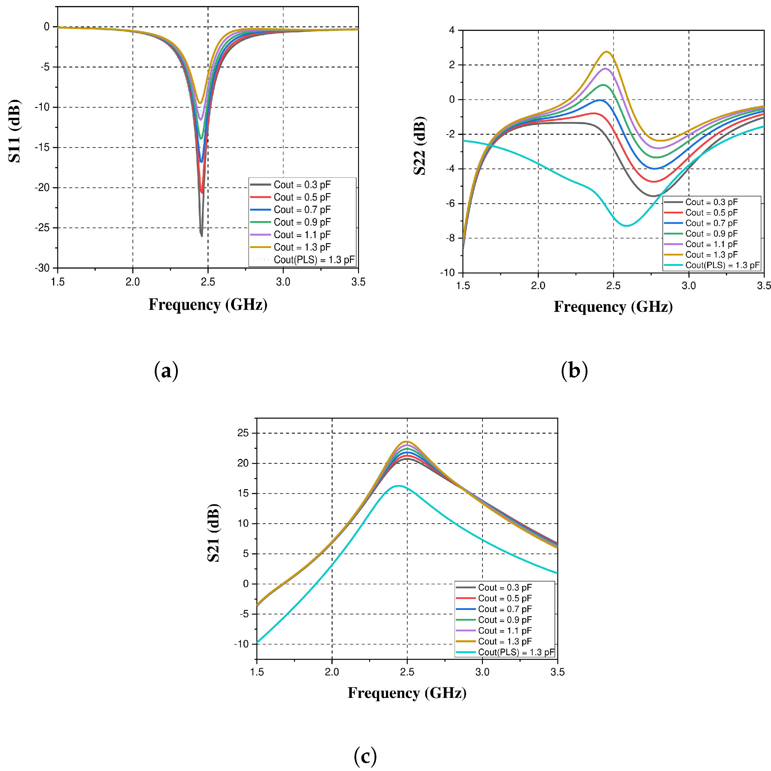
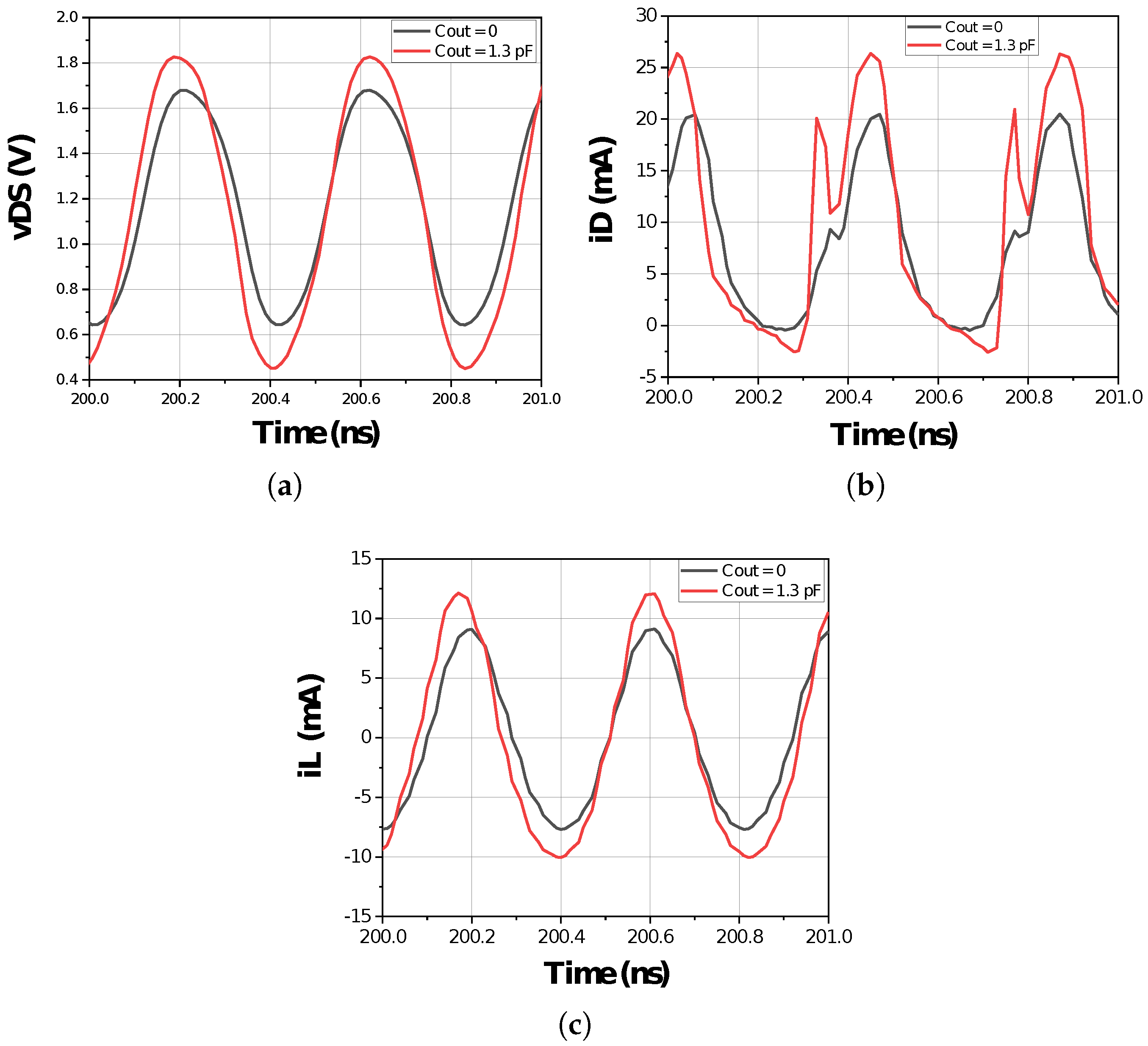
Before tackling the effect of lossy components in this section, it is necessary to point out that optimizations to the layout have led to the suppression of the inductance L T of the PA because the output matching can only be ensured by the output network effect associated with capacitance C T . In addition, post-layout simulations were performed with an extreme capacitance value ( C o u t = 1.3 pF). As shown in Figure 8a, the added output capacitance C o u t increased the insertion loss in the PA’s input and output by 16 dB and 5 dB, respectively, even when considering an impedance transformation between an optimal resistance R o p t and an R L of 50 ohm. This would be essentially due to the mismatches in the input–output impedances while varying C o u t . Such an effect could be overcome using variable capacitances as varactors in the input–output matching networks. In contrast to real component simulations, where S 22 is superior to 0, as seen in Figure 8b, PLSs reveal S 22 6 dB ( C o u t = 1.3 pF) without L T . Moreover, an advantage of this work is the improvement in S 21 by 4 dB, as shown in Figure 8c, while tuning the added capacitor. A maximal value of C o u t = 1.3 pF should decrease in hand the harmonic network impedance Z n e t and therefore decrease the total output impedance Z t o t to reduce the dissipate power in the other hand. However, C o u t causes mismatches in the output matching network as a drawback of the added capacitor. The effect of C o u t is also significant for the drain waveforms, as shown in Figure 9a,b. In fact, during the positive half-cycle, the drain voltage attains a maximal value of 1.8 V whereas the minimal value of the drain current is 0 mA. In the second half-period, the maximal value of the drain current is 26 mA while the minimal value of the drain voltage is 0.48 V. As a result, the dissipate power will decrease, allowing for the efficiency to increase. Furthermore, the load current is large with the added capacitor C o u t , as illustrated in Figure 9c, leading to a higher output power and power gain. However, the only observed drawback in Figure 9 is a fast shift in the operating frequency between the waveforms extracted by C o u t null and C o u t , equal to 1.3 pF. Such a shift is the effect of C o u t in the output matching network.

3.1. Performance of Real Class-F Power PAs

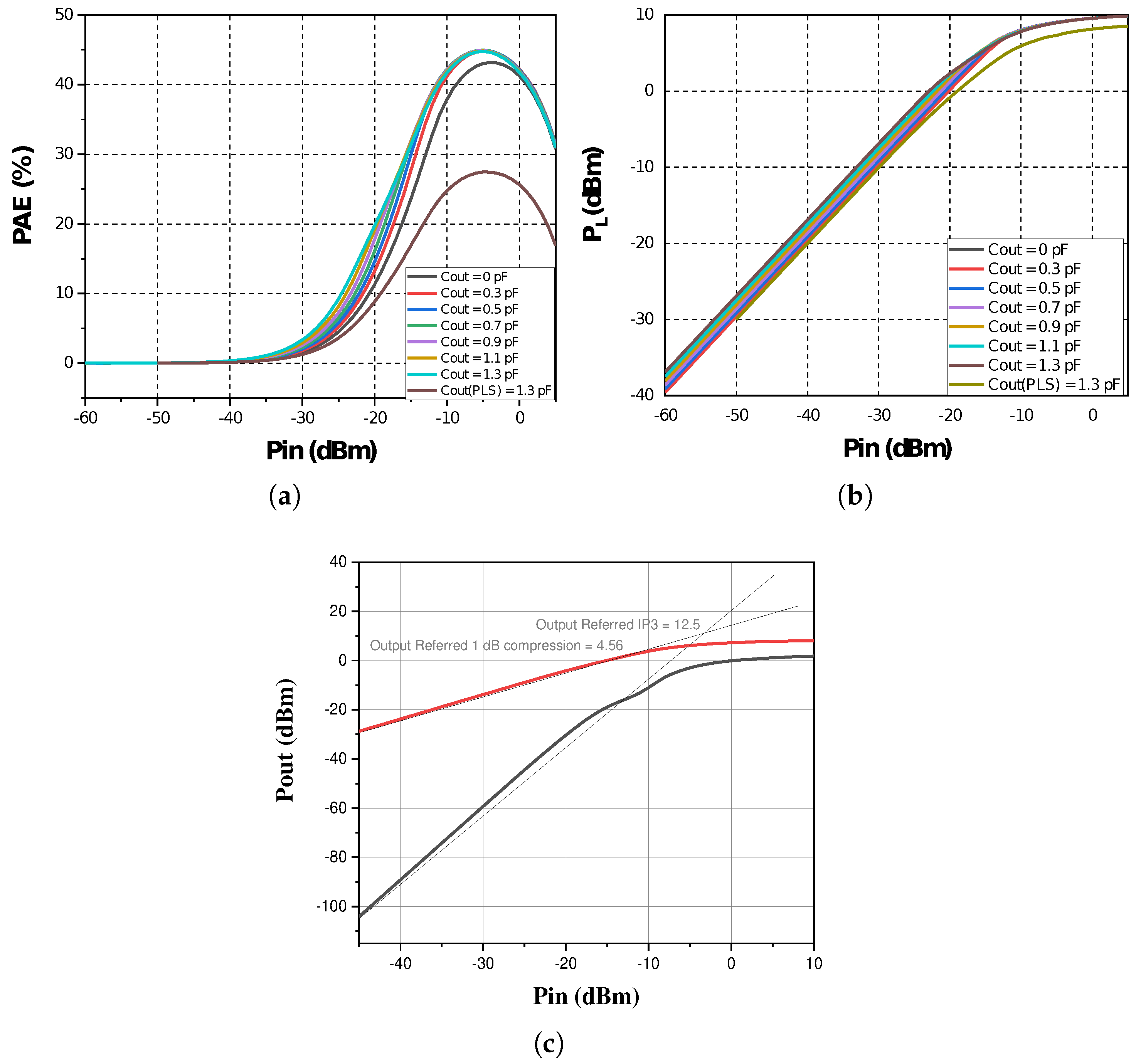
The most important results of this work are demonstrated in this section, where the key output parameters of the designed class-F power amplifier are presented. In Figure 10a, we can observe that, in the back-off region between −30 dBm and −10 dBm, the maximum PAE increased by 10% for Pin = −20 dBm. This can be observed while taking the input–output impedance mismatches due to C o u t into consideration. Moreover, the saturated efficiency PAE also increased from 43% ( C o u t = 0 ) to 45% ( C o u t = 1.3 pF). In Figure 10b, the power gain is shown to be quite flat. Second, the added output capacitor C o u t did not have any effect on the compressed output power P L (−1 dB), which remains practically constant. Furthermore, it increases for P i n = −40 dBm, from −21 dBm ( C o u t = 0 ) to −16 dBm ( C o u t = 1.3 pF) and for P i n = −20 dBm from −1 dBm ( C o u t = 0) to 3 dBm ( C o u t = 1.3 pF). Similarly, for P i n = −20 dBm, the power gain increased from 18 dB ( C o u t = 0) to 23.7 dB ( C o u t = 1.3 pF). In other words, the output power is enhanced in the power back-off region.
Post-layout simulations showed a compressed load power point P L (−1 dB) of around 4.56 dBm and an output third-order intercept point OIP3 at 12.5 dBm, respectively, compared to the only article [17] that considers linearity as a criterion, which reported an OIP3 equal to 25.4 dBm for a P L (−1 dB) of 20.2 dBm. These two parameters indicate the good linearity of the designed PA, as depicted in Figure 10c. Furthermore, a power gain G p of 20 dB and a significant degradation in the added power efficiency (PAE) to 28% are noted, due to the resistive losses in implemented inductances in the layout. Such a phenomenon is observed in other reported designs, such as [5,16,19].

3.2. Layout of the Designed Class-F Power Amplifier

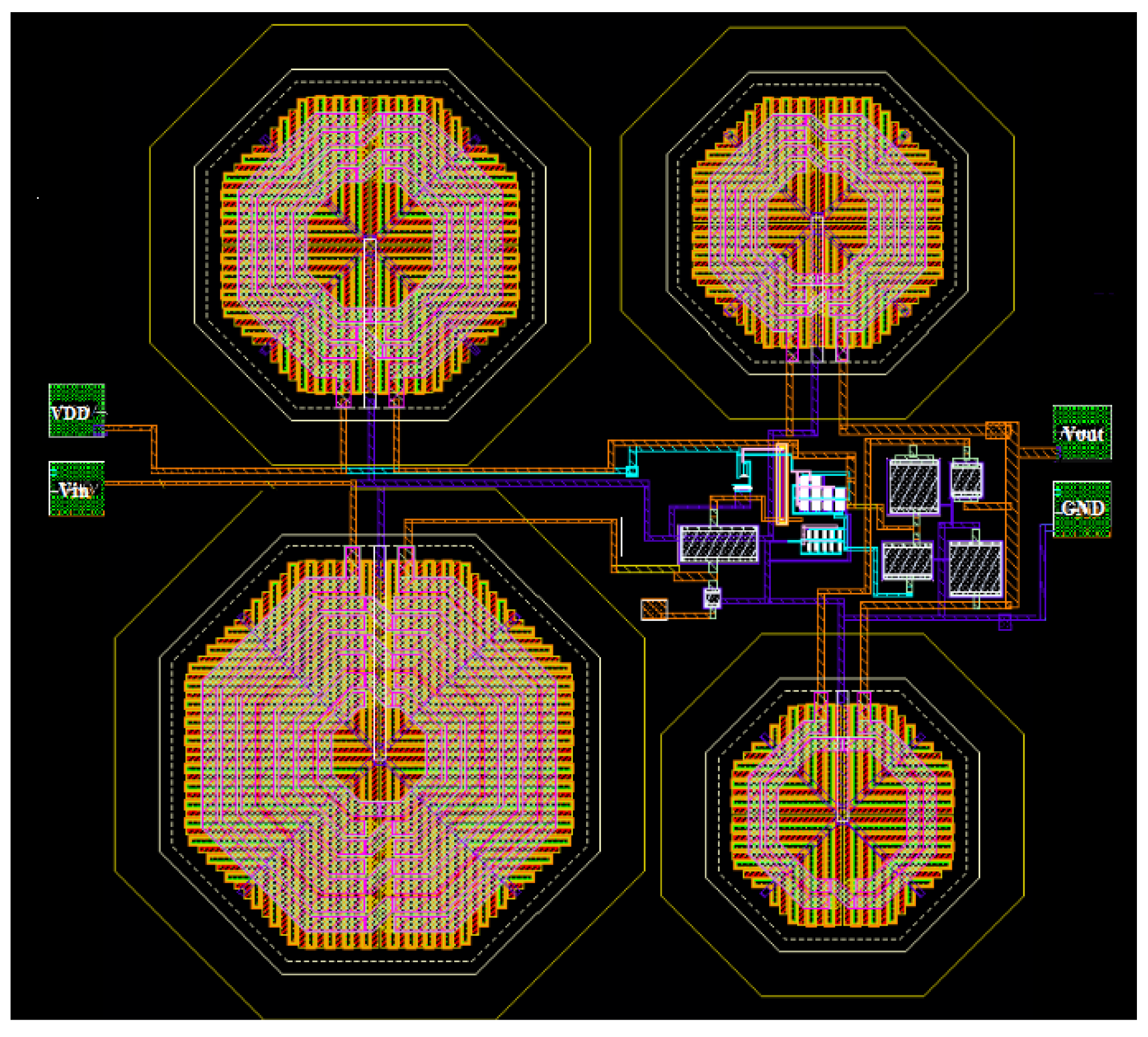
Simulations were carried out using the Cadence virtuoso 6 Calibre simulator, with the 0.13   μ m BiCMOS design kit as a process. As shown in Figure 11, the designed class-F PA has an active area of 732 × 605   μ m 2 . Unfortunately, the four inductances occupy most of that surface, especially the seven-turn inductance L M of 7.78 nH with a series resistance R S 5 Ohm. In reality, the surface occupied by the inductances represents more than 60% of the total chip area, which leads to more resistive losses and more restrictions during the design rules check (DRC step), the reason for the inductance L T suppression. Parasitic extraction was performed by quantus QRC instead of EM simulations to display RLC parasitics.
In this layout, we utilized all six metallic levels that were allowed with 0.13   μ m BiCMOS technology. More precisely, thin metals 1 and 2 were employed to ensure the (ground and supply) connections of the circuit. Thick metal 6 was used to transport the RF signal from the input to the output of the PA while ensuring the shortest connection. Metals 3, 4 and 5 were used to connect the different components in the circuit. Note that pads were not used in this layout because the designed PA was intended to be implemented on an overall transmitter dedicated to IoT application. Therefore, post-layout simulations were ensured through specific input/output layers.
Table 2 compares the performance of the designed class-F power amplifier and existing designs reported in the technical literature. All the presented PAs are based on a class-F CMOS, except for the work reported in [21], which was designed with SiGe 0.13 um technology and adopts an inverse class-F as the operating class.
Furthermore, all reported works adopted the tuned output network approach (via harmonic or matching circuits).
In the results, the PAE of the designed PA attained a good saturated level of 45% (28% for the post-layout simulations), allowing for an increase in the overall efficiency in the back-off region of between 5% and 10%. This is slightly significant compared to the PA in [5], designed using 0.18   μ m CMOS technology, where inductances cover a small area, consequently causing a weak loss. Otherwise, the maximal output power reaches 19.5 dBm for a power gain of 11.5 dB and a higher supply voltage of 4 V. Employing feedback formed of an inductance–capacitance series in [7] allows for the preservation of the drain voltage in a saturated region, enhancing the efficiency to attain 34.2 for an LTE output power level of 26.7 dBm and a power gain of 31.2 dB. This performance is good regarding the operating frequency and supply voltage.
Compared to [8], a high efficiency of 42% was observed for a switching class-F PA designed with CMOS 40 nm technology. Conversely, a very low debited power of −20 dBm was observed, even if the output-matching network and filter were merged. As for the results in [10], post-layout simulations demonstrated a higher peak efficiency of 68% for a saturated output power of 27 dBm, thanks to an output network based on multi-mode operation using RF choke inductance, a second harmonic branch, and a transformer-balun, permitting a decrease in the drain impedance. However, the only drawback is the area occupied by the whole circuit. The design reported in [17], adopting a class-AB driver and class-F power stage structures, expressed a measured efficiency of 24.4% for a saturated output power of 21 dBm and a power gain of 13.1 dB to meet WiMAX features. Therefore, a PA of an output network designed with transformer lines was implemented over a chip area of 0.99 mm 2 , except the third harmonic branch, which was mounted off-chip. Nevertheless, the consumption power of 716 mW is very high for this kind of application. Similar to our PA, a reported work [20] designed differential class-F modes under two blocs (Driver + Power stage); the saturated efficiency was 29.5% for a saturated output power of 23 dBm and a power gain of 24 dB. The circuit was totally integrated and implemented over a chip area of 0.53 mm 2 , which seems acceptable. Otherwise, this circuit consumes a huge amount of power at 136 mW. Ref. [22] reported a class-F PA designed with CMOS 0.153 μ m technology that expressed a saturated efficiency of 35% for a peak output power of 31.3 dBm and a power gain of 35.3 dB, constituting a very high performance regarding the power splitting–combining technique that experiences high power at the load level in order to cover different transmission standards. The PA is implemented on a chip area of under 2.9 mm 2 , taking into account the employed transformers. The switching class-F PA reported in [24] demonstrated a measured saturated efficiency of 26.1% for a saturated output power of 6 dBm, drawing a weak power consumption of 15.3 mW with a small chip surface of 0.39 mm 2 . Finally, article [25], where the class-F PA is based on a splitter–combiner transformer topology, showed important results in the measured efficiency, which equalled 32% for an output power and power gain of 27.8 dBm and 11.6 dB, respectively. However, this circuit has a significant power consumption of 158 mW and occupies a large chip surface of 2.32 mm 2 . In summary, compared with the different works reported in Table 2, this contribution, in addition to adding a current harmonic component, presents the advantage of improving the PA performance by modulating the drain–bulk capacitance, with an efficiency of 10%, an output power of 5 dBm and a power gain of 5 dB in the back-off region. Moreover, our circuit consumes a small amount of power (about 6 mW) and is implemented on a surface of 0.43 mm 2 , representing a good performance. Upon analysis of the figure of merit (ITRS FOM) related to our PA, which is equal to 35.05, it seems very low compared to the others reported in Table 2, which can be attributed to the weak output power and low operating frequency values of our design.

4. Conclusions

In this work, an integrated class-F power amplifier, dedicated to low-power I-Q amplitude modulation wireless transceivers with a modulated added output capacitor parallel with cascode transistor, was successfully designed. At first, a theoretical analysis was performed, considering lossless components, to investigate the effect of an added capacitor on the PA performance. In fact, adding and varying this capacitor led to the creation of a new second current harmonic that participates in shaping the drain’s voltage-current waveforms at the cascode transistor level to reduce the dissipative drain power. By using cadence tools to simulate the added capacitor’s impact on the PA, the results demonstrated an enhancement of output power by 8 dBm, power gain of 19 dB, and power-added efficiency from 40 to 45, and again by (+5 dBm), (+5 dB) and (+5% to 10%) in the power back-off region from −30 to −10 dBm, respectively. Post-layout simulations (PLS) were performed on the designed class-F PA to reveal an improvement in load power of 5 dBm ( 50 dBm P B O 20 dBm , 8 dBm ) power gain of 20 dB (+5 dB in the same PBO), overall efficiency of from 5 to 10% ( 50 dBm P B O 15 dBm , and 28% for C o u t = 1.3 pF. The designed class-F PA was implemented over a chip area of 732 × 605   μ m 2 . Accordingly, the previously highlighted trade-offs can be avoided by designing miniaturized efficient class-F PA useful in the linear transceivers.

Author Contributions

Conceptualization, S.T.; Methodology, S.T., M.T. and M.C.E.Y.; Validation, M.T. and M.C.E.Y.; Formal analysis, S.T. and M.C.E.Y.; Investigation, M.T. Writing—original draft, A.B. and M.C.E.Y. All authors have read and agreed to the published version of the manuscript.

Funding

This research received no external funding.

Data Availability Statement

Not applicable.

Conflicts of Interest

The authors declare no conflict of interest.

References

  1. Niknejad, A.M.; Chowdhury, D.; Chen, J. Design of CMOS power amplifiers. IEEE Trans. Microw. Theory Tech. 2012, 60, 1784–1796. [Google Scholar] [CrossRef]
  2. Cripps, S.C. RF Power Amplifiers for Wireless Communications; Artech House: Norwood, MA, USA, 2006; Volume 2. [Google Scholar]
  3. Kazimierczuk, M.K. RF Power Amplifiers; John Wiley & Sons: Hoboken, NJ, USA, 2014. [Google Scholar]
  4. Im, D.; Kwon, K.; Lee, I.Y. A 1.9-GHz silicon-on-insulator CMOS stacked-FET power amplifier with uniformly distributed voltage stresses. Int. J. Circuit Theory Appl. 2017, 45, 1660–1672. [Google Scholar] [CrossRef]
  5. Gilasgar, M.; Barlabé, A.; Pradell, L. A 2.4 GHz CMOS class-F power amplifier with reconfigurable load-impedance matching. IEEE Trans. Circuits Syst. I Regul. Pap. 2018, 66, 31–42. [Google Scholar] [CrossRef] [Green Version]
  6. Ali, S.N.; Agarwal, P.; Baylon, J.; Heo, D. Reconfigurable high efficiency power amplifier with tunable coupling coefficient based transformer for 5G applications. In Proceedings of the 2017 IEEE MTT-S International Microwave Symposium (IMS), Honololu, HI, USA, 4–9 June 2017; pp. 1177–1180. [Google Scholar]
  7. Kim, J.H.; Park, C.S. A feedback technique to compensate for AM-PM distortion in linear CMOS class-F power amplifier. IEEE Microw. Wirel. Compon. Lett. 2014, 24, 725–727. [Google Scholar] [CrossRef]
  8. Iguchi, S.; Saito, A.; Watanabe, K.; Sakurai, T.; Takamiya, M. Design Method of Class-F Power Amplifier With Output Power of -20 dBm and Efficient Dual Supply Voltage Transmitter. IEEE Trans. Circuits Syst. I Regul. Pap. 2014, 61, 2978–2986. [Google Scholar] [CrossRef]
  9. Ma, C.; Liu, Y.; Pan, W.; Tang, Y. 0.4–3.0 GHz highly efficient harmonic-tuned power amplifier. Electron. Lett. 2015, 51, 1911–1913. [Google Scholar] [CrossRef]
  10. Kumaran, A.K.; Pashaeifar, M.; D’Avino, M.; de Vreede, L.C.; Alavi, M.S. On-chip output stage design for a continuous class-F power amplifier. In Proceedings of the 2021 IEEE International Symposium on Circuits and Systems (ISCAS), Daegu, Republic of Korea, 22–28 May 2021; pp. 1–5. [Google Scholar]
  11. Raab, F.H. Class-F power amplifiers with maximally flat waveforms. IEEE Trans. Microw. Theory Tech. 1997, 45, 2007–2012. [Google Scholar] [CrossRef]
  12. Sharma, T.; Darraji, R.; Ghannouchi, F.; Dawar, N. Generalized continuous class-F harmonic tuned power amplifiers. IEEE Microw. Wirel. Compon. Lett. 2016, 26, 213–215. [Google Scholar] [CrossRef]
  13. Carrubba, V.; Akmal, M.; Quay, R.; Lees, J.; Benedikt, J.; Cripps, S.C.; Tasker, P.J. The continuous inverse class-F mode with resistive second-harmonic impedance. IEEE Trans. Microw. Theory Tech. 2012, 60, 1928–1936. [Google Scholar] [CrossRef]
  14. Lu, Z.; Chen, W. Resistive second-harmonic impedance continuous class-F power amplifier with over one octave bandwidth for cognitive radios. IEEE J. Emerg. Sel. Top. Circuits Syst. 2013, 3, 489–497. [Google Scholar] [CrossRef]
  15. Sessou, K.K.; Neihart, N.M. An Integrated 700–1200-MHz Class-F PA With Tunable Harmonic Terminations in 0.13 um CMOS. IEEE Trans. Microw. Theory Tech. 2015, 63, 1315–1323. [Google Scholar] [CrossRef]
  16. Ye, L.; Chen, J.; Kong, L.; Alon, E.; Niknejad, A.M. Design considerations for a direct digitally modulated WLAN transmitter with integrated phase path and dynamic impedance modulation. IEEE J. Solid-State Circuits 2013, 48, 3160–3177. [Google Scholar] [CrossRef]
  17. Liao, H.Y.; Chen, J.H.; Chiou, H.K.; Wang, S.M. Harmonic control network for 2.6 GHz CMOS class-F power amplifier. In Proceedings of the 2009 IEEE International Symposium on Circuits and Systems, Taipei, Taiwan, 24–27 May 2009; pp. 1321–1324. [Google Scholar]
  18. Hu, S.; Kousai, S.; Wang, H. 2.8 A broadband CMOS digital power amplifier with hybrid class-G Doherty efficiency enhancement. In Proceedings of the 2015 IEEE International Solid-State Circuits Conference-(ISSCC) Digest of Technical Papers, San Francisco, CA, USA, 22–26 February 2015; pp. 1–3. [Google Scholar]
  19. Love, M.; Thian, M.; Grebennikov, A. A 5-GHz Class-E3F2 power amplifier with 51% PAE and 21-dBm output power on 65nm CMOS. In Proceedings of the 2017 IEEE 18th Wireless and Microwave Technology Conference (WAMICON), Cocoa Beach, FL, USA, 24–25 April 2017; pp. 1–4. [Google Scholar]
  20. Mansour, M.; Zekry, A.; Ali, M.K.; Shawkey, H. Analysis and Design of a 5G Multi-Mode Power Amplifier using 130 nm CMOS technology. In Proceedings of the 2021 22nd International Symposium on Quality Electronic Design (ISQED), Santa Clara, CA, USA, 7–9 April 2021; pp. 280–284. [Google Scholar]
  21. Dong, L.; He, S.; You, F.; Lei, Q. High-efficiency Class-F- 1 power amplifier design with input harmonic manipulation. In Proceedings of the 2012 IEEE Topical Conference on Power Amplifiers for Wireless and Radio Applications, Santa Clara, CA, USA, 15–18 January 2012; pp. 1–4. [Google Scholar]
  22. Tsai, M.D.; Lin, C.C.; Chen, P.Y.; Chang, T.Y.; Tseng, C.W.; Lin, L.C.; Beale, C.; Tseng, B.; Tenbroek, B.; Chiu, C.S.; et al. 13.1 A fully integrated multimode front-end module for GSM/EDGE/TD-SCDMA/TD-LTE applications using a Class-F CMOS power amplifier. In Proceedings of the 2017 IEEE International Solid-State Circuits Conference (ISSCC), San Francisco, CA, USA, 5–9 February 2017; pp. 216–217. [Google Scholar]
  23. Chakrabarti, A.; Krishnaswamy, H. High-power high-efficiency class-E-like stacked mmWave PAs in SOI and bulk CMOS: Theory and implementation. IEEE Trans. Microw. Theory Tech. 2014, 62, 1686–1704. [Google Scholar] [CrossRef]
  24. Peng, X.; Yin, J.; Mak, P.I.; Yu, W.H.; Martins, R.P. A 2.4-GHz ZigBee Transmitter Using a Function-Reuse Class-F DCO-PA and an ADPLL Achieving 22.6% (14.5%) System Efficiency at 6-dBm (0-dBm) Pout. IEEE J. Solid-State Circuits 2017, 52, 1495–1508. [Google Scholar] [CrossRef]
  25. Chen, F.; Wang, Y.; Hsiao, Y.H.; Lin, J.L.; Chen, Y.C.; Wang, H. A 4.6-GHz Class-F- 1 high power CMOS power amplifier. In Proceedings of the 2017 IEEE International Symposium on Radio-Frequency Integration Technology (RFIT), Seoul, Republic of Korea, 30 August–1 September 2017; pp. 183–185. [Google Scholar]
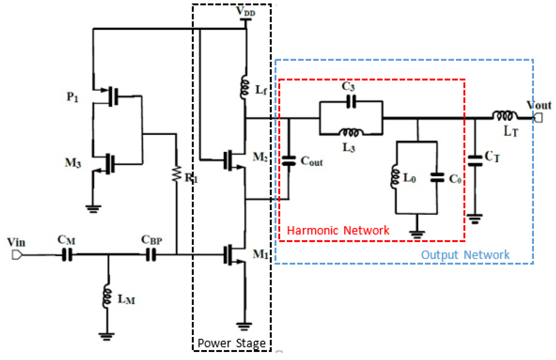
Figure 1. Proposed structure of a class-F power amplifier.
Electronics 12 02784 g001
Figure 2. Structure of the class-F power amplifier (dynamic form).
Electronics 12 02784 g002
Figure 3. Real part of class-F PA input impedance over a frequency range.
Electronics 12 02784 g003
Figure 4. Impedances Z n e t and Z t o t . (a) at fundamental frequency. (b) at the third harmonic. (c) at fundamental frequency and (d) at the third harmonic.
Electronics 12 02784 g004
Figure 5. Dissipate power and drain voltage and current versus C o u t for P i n = −22 dBm. (a) Dissipate power P D ( ω ) . (b) Drain voltage with C o u t variations at f 0 = 2.45 GHz. (c) Drain current with C o u t variations at f 0 = 2.45 GHz.
Electronics 12 02784 g005
Figure 6. Drain voltage–current fundamental and harmonic components versus C o u t for P i n = −22 dBm. (a) Fundamental component of drain voltage. (b) Fundamental component of drain current. (c) Third harmonic component of drain voltage. (d) Second harmonic component of drain current.
Electronics 12 02784 g006
Figure 7. Current at load level, and efficiency of the class-F PA as a function of C o u t for P i n = 22 dBm. (a) Output current at load level with frequency variations. (b) Drain efficiency η and power-added efficiency PAE as a function of C o u t .
Electronics 12 02784 g007
Figure 8. S parameters as function of C o u t for P i n = −15 dBm. (a) S 11 . (b) S 22 . (c) S 21 .
Electronics 12 02784 g008
Figure 9. Drain and load waveforms with and without C o u t , f 0 = 2.45 GHz. (a) Drain voltage waveforms. (b) Drain current waveforms. (c) Load current waveforms.
Electronics 12 02784 g009
Figure 10. Class-F PA performance as a function of C o u t at f 0 = 2.45 GHz. (a) PAE. (b) Output power P L and power gain G p . (c) P L (-1dB) and third designed class-F PA.
Electronics 12 02784 g010
Figure 11. Layout of the designed class-F power amplifier with an area of 732 × 605   μ m 2 .
Electronics 12 02784 g011
Table 1. Proposed class-F PA amplifier: design parameters.
Parameter V D D
(V)
η (max)
%
P D C
(dBm)
V g s 0
(V)
C o x
(pF/m 2 )
C o v
(fF)
C M
(pF)
L M
(nH)
C g s 1
(pF)
C g s 2
(pF)
C g d 1
(pF)
C g d 2
(pF)
C d b 1
(pF)
Value1.27080.240.0140.140.1757.784.240.480.0180.0561.176
Parameter C d b 2
(pF)
L f
(nH)
L 3
(nH)
C 3
(pF)
L 0
(nH)
C 0
(pF)
L T
(nH)
C T
(pF)
r d s 1
( Ω )
r d s 2
( Ω )
g m 1
(mA/V)
g m 2
(mA/V)
R o p t
( Ω )
Value0.4242.40.6420.7361.912.221.260.5551.17.10 7 5.6.10 4 0.380.128130
Table 2. Comparison of this work with state-of-the-art methods (***: measured values, **: post-layout simulation values. *: ITRS FOM = PSAT (dBm) + Gain (dB) + 20log10 (Freq (GHz)) + 10log10 (PAE)) [23].
Ref.TechnologyFrequency
(GHz)
VDD
(V)
PDC
(mW)
PL
(dBm)
GP
(dB)
PAE
(%)
Area (mm 2 )ClassITRS
FOM
Technique
[5] 0.18   μ m
CMOS
2.43–4-18.7 **
19.5 ***
(Sat)
10.2 **
11.5 ***
28.9 **
26 ***
2.56F32.75- Reconfigurable
load-impedance
matching.
 [7]0.18 μ m
CMOS
0.8693.3-26.7 ***
(max)
31.2 ***34.2 ***1.496F-- Off-chip OMN
and feedback.
 [8]40 nm
CMOS
2.40.56–0.2-−20 ***
(Sat)
-42 ***0.3F-- Merging OMN and Filter
to improve an output
power.
[10]40 nm
CMOS
2.42.7-27 **
(Sat)
-68 **
(Sat)
-F-- Design of CCF PA with
Transformer Balun,
RF Shock, 2nd Harmonic
Branch.
[17]0.18 μ m
CMOS
2.61.8716.4≈21 ***
(sat)
13.1 ***24.4 ***0.998F36.27- Tunable harmonic
termination.
[20] 0.13   μ m
CMOS
4.83136/2623/22.3 **
(Sat)
24/27 **29.5/28.6 **
(Sat)
0.53F55.32- Linear/switching
modes
with tuning
output network.
 [22]153 nm
CMOS
2.43.5-31.5 ***
(Sat)
35.3 ***35 ***2.9F-- GSM/EDGE/TD-
SCDMA/TD-LTE
by transformer
combination.
 [24]65 nm
CMOS
2.40.3–0.715.3
(Sat)
6 ***
(Sat)
26.1 ***
(Sat)
0.39F-- Function reuse
class-F DCO-PA
+ ADPLL.
 [25] 0.18   μ m
CMOS
4.63.615827.8 ***
(Sat)
11.6 ***32 ***
(Sat)
2.32F47.71- Differential
topology based
on the transformer
combiner.
This
work
0.13   μ m
BiCMOS
2.41.25–88 **(Sat)
(+5 PBO)
4.56 **
P L (−1 dB)
20 **
(+5 PBO)
28 **
(+10 PBO)
0.43F35.05- Tuned output
network by
cascode stage output
capacitor modulation.
Disclaimer/Publisher’s Note: The statements, opinions and data contained in all publications are solely those of the individual author(s) and contributor(s) and not of MDPI and/or the editor(s). MDPI and/or the editor(s) disclaim responsibility for any injury to people or property resulting from any ideas, methods, instructions or products referred to in the content.