Article

Ultra-Low-Power Compact Neuron Circuit with Tunable Spiking Frequency and High Robustness in 22 nm FDSOI

1
Institute of Microelectronics of the Chinese Academy of Sciences, Beijing 100029, China
2
University of Chinese Academy of Sciences, Beijing 100029, China
3
Key Laboratory of Science and Technology on Silicon Devices, Chinese Academy of Sciences, Beijing 100029, China
*
Author to whom correspondence should be addressed.
Electronics 2023, 12(12), 2648; https://doi.org/10.3390/electronics12122648
Submission received: 24 May 2023 / Revised: 7 June 2023 / Accepted: 9 June 2023 / Published: 13 June 2023
(This article belongs to the Section Microelectronics)

Abstract

:
Recent years have seen an increasing popularity in the development of brain-inspired neuromorphic hardware for neural computing systems. However, implementing very large scale simulations of neural networks in hardware is still an open challenge in terms of power efficiency, compactness, and biophysical resemblance. In an effort to design biologically plausible spiking neuron circuits while restricting power consumption, we propose a new subthreshold Leaky Integrate-and-Fire (LIF) neuron circuit designed using 22 nm FDSOI technology. In this circuit, problems of large leakage currents and device mismatch are effectively reduced by deploying the back-gate terminal of FDSOI technology for a tunable design. The proposed neuron is able to operate in two spiking frequency modes with tunable bias parameter setting of key transistors, and it results in complex firing behaviors, such as adaptation, chattering, and bursting, through varying bias voltages. We present circuit post-layout simulation results and demonstrate the biologically plausible neural dynamics. Compared with published state-of-the-art neuron circuits, the circuit dissipates ultra-low energy per spike, on the order of femtojoules per spike, at firing rates ranging from 30 Hz to 1 kHz. Furthermore, the circuit is proven to maintain a good robustness over process variation and Monte Carlo analysis, with relative error 3.02% at a firing rate of approximately 67.1 Hz.

1. Introduction

The sophistication of artificial neural networks (ANNs) algorithms is constantly advancing. However, traditional Von Neumann-based computers are plagued by “storage access bottlenecks”, leading to inefficient computing abilities and high power consumption that fall short of the demands posed by complex AI algorithms [1,2,3]. In order to solve these problems, brain-inspired spiking neural networks (SNNs) have emerged as the third generation of ANNs, mimicking biological brain processes in hardware [4,5,6,7,8,9]. The basic computing unit in a spiking neural network is the neuron, which communicates with its peers via synapses using electrical impulses known as spikes [10,11,12,13].
Several brain emulation engines have been developed, based on mixed-signal neuromorphic circuits, to improve the efficiency of brain-inspired computing [14,15,16]. To emulate brain-like functionality, a very large number of neurons are required in SNNs. As a result, neuron cells are considered as an efficient component with respect to saving power consumption and silicon real estate [17,18,19]. This also highlights the need for simple neuron circuits with a minimum number of transistors and high computing efficiency. Over the last few decades, the Resonate and Fire [20], Hindmarsh–Rose [21], Mihalas–Niebur, and Izhikevich [22,23] models have been the primary sources of inspiration for the development of next-generation neuromorphic circuits. Of all neuron models, the Leaky Integrate-and-Fire (LIF) neurons are claimed to be compact and more computationally efficient. Nevertheless, standard design methods of LIF neurons do not provide adequate firing behaviors and lead to bulky areas and high power consumption. Therefore, various circuits such as voltage-amplifier, tau-cell, low-pass filter (LPF), and differential pair integrator (DPI) have been used to develop and generalize the operation of the traditional neurons [24,25,26,27]. Moreover, the circuitry parts of a DPI-based subthreshold neuron presented in [24,25] can be reconfigured using the simplest low-voltage analog circuits to offer a silicon neuron with the capability of operating under ultra-low-voltage supplies, which provides the potential for subthreshold neuron circuit design.
To solve the energy issue, transistors are preferably biased in the subthreshold region. However, nano-scale CMOS devices suffer from significant leakage currents and device mismatch issue in subthresholds [28]. Hence, emerging technologies such as Fully Depleted Silicon on Insulator (FDSOI) have emerged that show superior performance in leakage and power consumption [29,30]. Using back-gate bias is a new possibility in FDSOI technology to tune circuit performance. In this paper, for the first time, a novel neuron design is introduced that utilizes a 22 nm FDSOI process. This design allows the back-gate voltage to modulate the spiking frequency of the compact LIF neuron, while keeping the leakage unaffected. The neuron operates in the subthreshold region, which can display complex firing behaviors, and consumes an ultra-low energy per spike on the order of a few femtojoules. The final layout of the core neuron is only 484 μm2 in size.
The rest of this paper is organized as follows: Section 2 demonstrates the feasibility of implementing biophysically complex neural dynamics using ultra-low-power analog circuits in advanced scaled FDSOI processes, while also addressing leakage currents and device mismatch effects in neuron design. An analysis of the neuron operation and post layout optimization is also presented in Section 2. Post-layout simulation analysis, including complex firing behavior and variable frequency operation through tunable bias parameter settings, is presented in Section 3. The paper also quantifies the impact of device mismatch through Monte Carlo analysis and validates neuron performance against process variations and parasitic components. Finally, Section 4 concludes this brief.

2. FDSOI-Based LIF Neuron Circuit

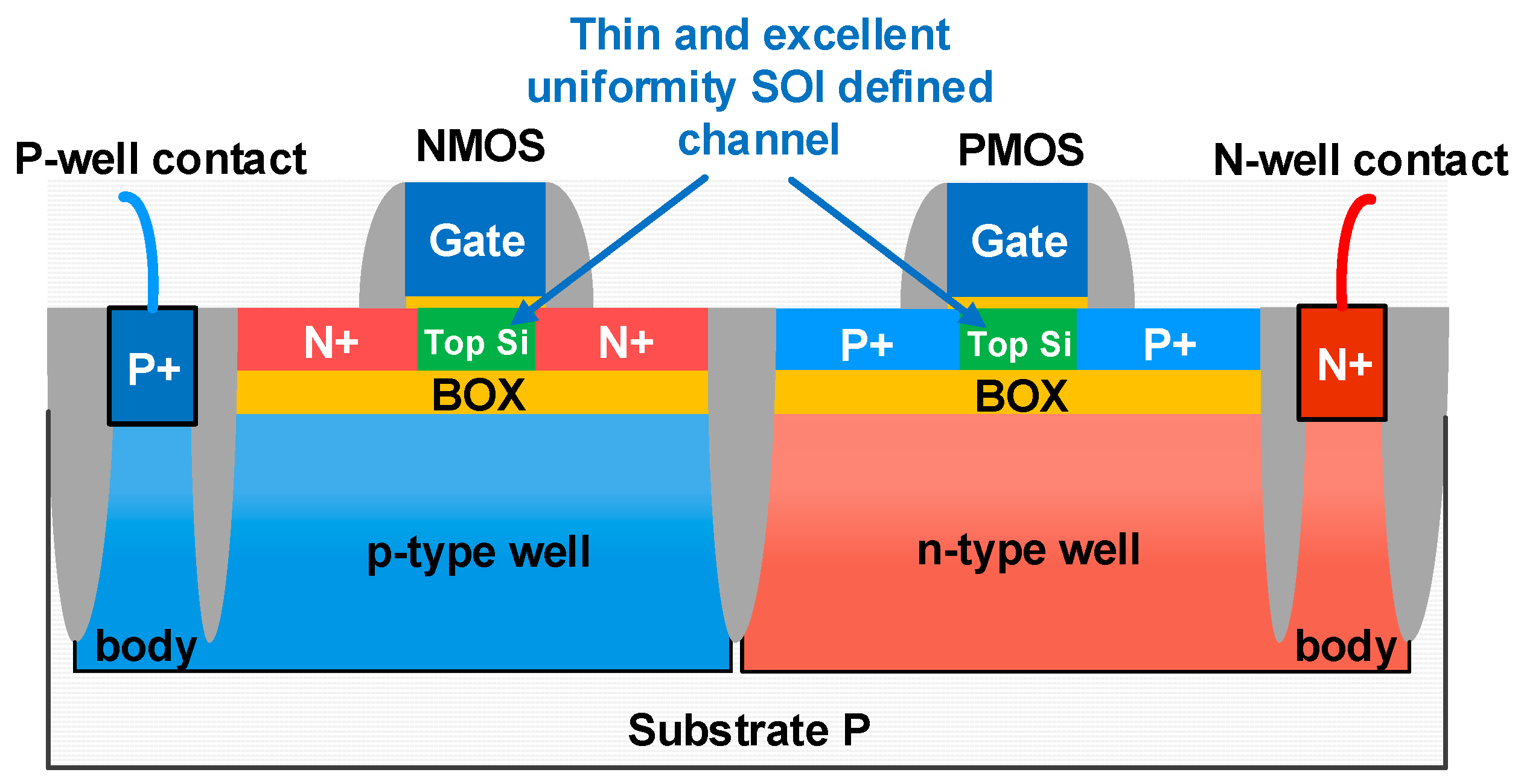
2.1. Advantages of FDSOI Technology in Neuron Circuit Design

Neuron circuits typically employ subthreshold-operated transistors with currents ranging from fractions of picoamperes to hundreds of nanoamperes [24,25,26,27,28,29,30]. However, non-ideal effects of advanced complementary metal–oxide–semiconductor (CMOS) technology nodes, such as drain-induced barrier lowering (DIBL), gate-induced drain leakage (GIDL), or random dopant fluctuation (RDF), can lead to leakage currents in the picoampere range and bring serious impacts for the functionality of subthreshold neuron circuits. The approach which utilizes above-threshold neuron circuit design has been proposed to mitigate leakage current effects; it can accelerate time constants by a factor of 1000 [31], but requires giving up the capacity to optimally process slowly changing synapse current signals. Another option is to employ switched capacitor techniques [32,33], which can increase circuit complexity and power consumption. Alternatively, one can leverage the capabilities of FDSOI technology. Figure 1 depicts the structural diagram of FDSOI devices. FDSOI technology adopts a thin buried oxide (BOX) insulating layer and shallow trench isolation to enhance electrical isolation between the thin and excellent uniformity channel and the substrate; this significantly mitigates bulk effects such as source/drain leakage, latch-up, parasitic capacitance of the source/drain junction, and substrate noise coupling. It is essential to stress that no latch-up effect occurs. The BOX layer structure of FDSOI devices enables the silicon layer to be fully depleted of charge carriers, providing better control over the threshold voltage and reducing leakage current, requiring less doping. The lower doping levels result in decreased threshold voltage variance and device mismatch in analog neuron circuits. In addition, the introduction of a second gate terminal allows improved channel control and reduced junction capacitance, referred to as “body” or “back-gate”. The back-gate can be biased forward or in reverse to optimize transistor performance in low leakage or high efficiency modes. We analyzed a 22 nm FDSOI PDK process that features two primary types of transistors with varying gate oxides—thin and thick. This affords designers a range of transistor models with differing threshold voltages and, thus, varied levels of leakage currents. In subthreshold neuron circuit designs, employing non-minimum size devices (i.e., large transistors) is often a necessary measure. For these cases, thick gate oxide devices need to be used to avoid gate leakage due to tunneling effects. Moreover, they can provide Low-Threshold-Voltage (LVT) and are typically flip-well devices with the same doping type for their well and channel. The threshold-voltage (Vth) and drain current (Id) can be further adjusted with back-gate biasing. For the neuron design, we utilized 1.2 V I/O thick gate oxide Low Threshold Transistors (LVT) with a Vdd of 0.4 V.
Figure 2 reveals simulated subthreshold IdVg characteristics of NMOS/PMOS devices with varying channel lengths. |Vds| is fixed at 400 mV and the device’s width is 1 µm. The drain current Id, ranging from picoamps to nanoamps, exhibits linear dependence on Vg. Figure 3 shows the IdVg characteristics of n-type and p-type FDSOI devices with W = 400 nm, L = 28 nm, and Vds = 400 mV, at different back-gate voltages Vbs of −400 mV, 0 V, and 400 mV. Seen here, higher values of Vbs result in smaller threshold voltage and greater drain current for NMOS devices, whereas the opposite effect occurs for PMOS.

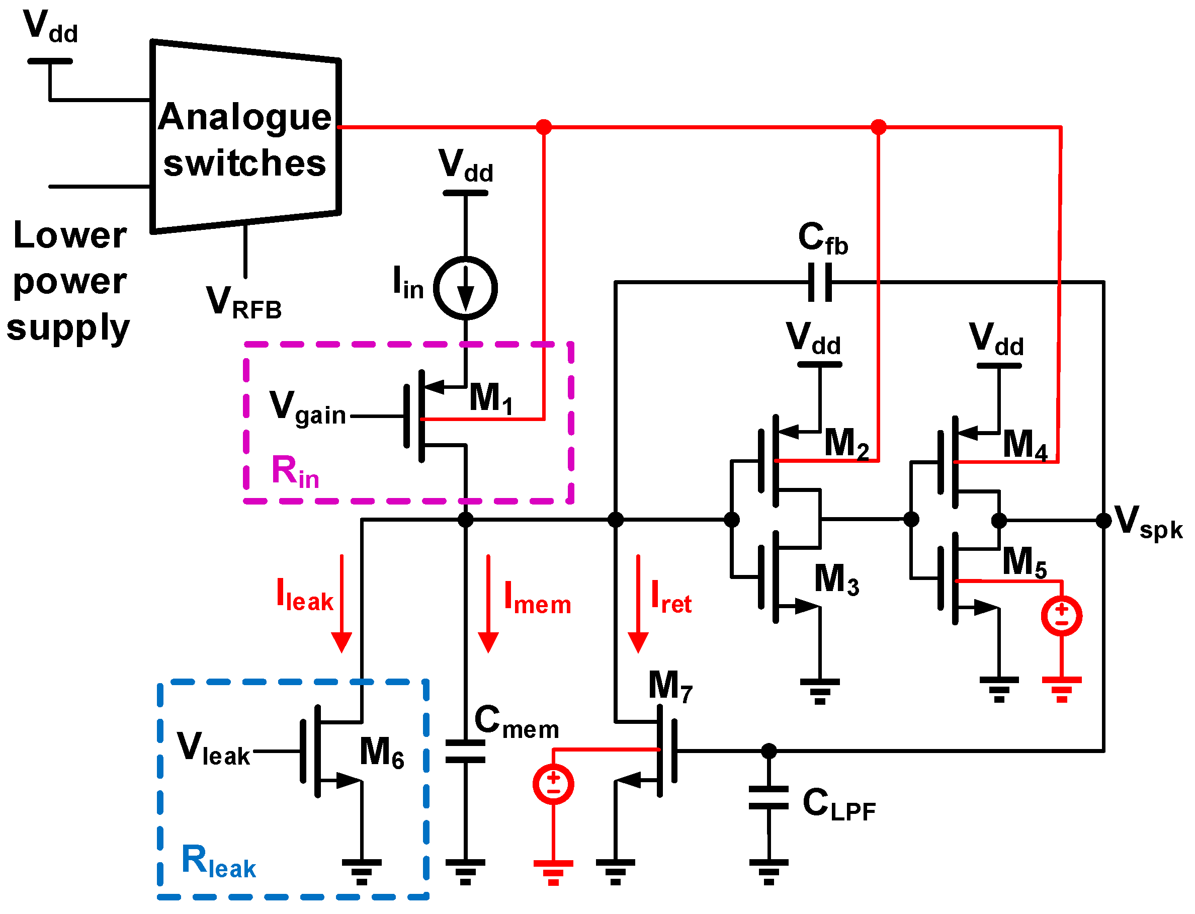
2.2. Proposed Method

The basic structure of the LIF neuron model is illustrated in Figure 4. Previous neuron spikes are received at the synapse and converted into a current that is multiplied by the synaptic intrinsic weight. This current is then integrated into the membrane potential capacitor Cmem. When the membrane potential exceeds the action potential of the neuron, a spike output is generated and transmitted to the subsequent neuron [13]. Following the spike, the neuron resets the membrane potential using a Low Pass Filter (LPF) circuit and waits for the next stimulus. Leaky path models the leakage conductance of the LIF neuron and provides a constant leakage current path Ileak. In addition, the presence of the leakage current path causes the membrane potential to decay over time if there is no input stimulus from the pre-neuron for an extended period.
The firing dynamics of LIF neurons are governed by Equations (1) and (2) [13]:
C m e m d V m e m t d t = I t V m e m t R
if   V m e m t > V t h r   then   V m e m t + Δ t > V R E T
where Vmem(t) represents membrane potential, Cmem is membrane capacitance, I(t) stands for the input current, R is the total leakage resistance of LIF neuron, Vthr is the threshold voltage, and VRET denotes the reset potential.
If a variable Ivar represents the current change in Imem and is generated due to mismatch issues in subthreshold region, the firing dynamics of the LIF neuron is primarily regulated by the current Ileak, which is determined by the resistance Rleak, while the reset current Iret is controlled by the output spike Vspk. Naturally, the firing rate of the neuron can deviate from its desired set value due to mismatch issues. These issues may result in a decrease in firing rate, likely caused by the number of leakage paths on the membrane capacitor of the neuron exceeding the number of charging paths. Additionally, if the external input current to the neuron remains constant, an increase in the bias voltage (e.g., Vthr) may also lead to a decrease in firing frequency. Consequently, maintaining a balance in the charging and discharging of neurons in the membrane capacitor to match the firing dynamics of neurons is critical for solving mismatch issues, particularly in compensating for leakage current paths.
C m e m d V m e m t d t = I i n I l e a k I r e t ± I v a r
While the leakage current cannot be decreased, the circuit can compensate for it by increasing the charging current of the membrane capacitor. A simplified diagram of the method is shown in Figure 5. If VRFB is at a low level, the analog switches are activated, and the back-gate bias of PMOS (M1, M2, M4) is set to a lower voltage to achieve a higher charge current (Imem). Otherwise, the back-gate bias must be connected to Vdd without the assistance of the tolerant circuit. The back-gate bias effect can adjust the transconductance of PMOS transistors. By isolating PMOS transistors in a well, the current in the path can be tuned to compensate for mismatches by varying the well voltage, as previously mentioned (refer to Figure 3). Moreover, we adjusted the back gate voltage of critical NMOS transistors using the unique advantages of the 22 nm FDSOI process. The aim was to prevent excessive compensation current from affecting the circuit, which greatly enhances the potential to regulate complex biologically realistic behaviors of neurons.

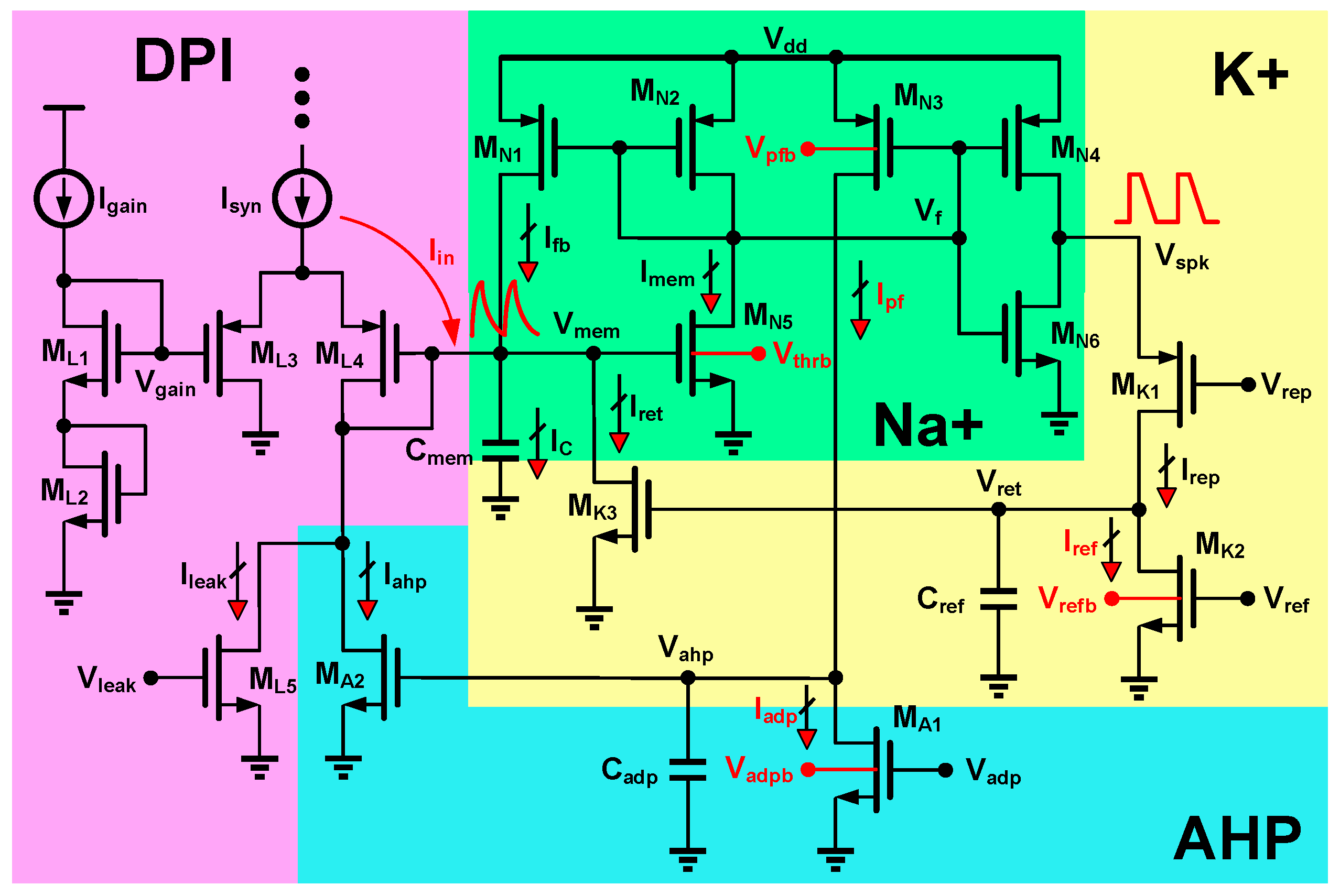
2.3. Proposed Subthreshold Neuron Circuit

The benefits of utilizing FDSOI technology in neuron circuit design, coupled with feasible design methods, have been previously explained. To simulate real environmental signals in SNN architectures, it is crucial to ensure that the neurons’ and synapses’ time constants reflect biologically plausible dynamics in circuit design. As described in [24], neuron conductance dynamics can be modeled by using first-order differential equations, which can be implemented via current-mode subthreshold circuits. Among such circuits, the differential pair integrator (DPI) provides a compact and low-power solution [24]. Unlike other approaches, such as log-domain low-pass filters and tau-cells [24], DPI circuit avoids transistors with bulk-source connections, resulting in a smaller silicon area and lower power consumption. Furthermore, DPI circuit is unaffected by any mismatches between its current sources. Thus, we employed a DPI circuit as an input current integrator. We proposed a wide range of spiking behavior LIF neuron circuits with adjustable spike frequency, which aim to provide optimal support for SNNs in terms of achieving remarkable learning and pulse coding performance [34]. The following text clearly discusses the design parameters, functions, and low-power design concept of the circuit.
The proposed neuron was designed with 22 nm FDSOI technology and the topology is shown in Figure 6. The supply voltage Vdd was set to 0.4 V for the subthreshold operation. The capacitances were realized using Alternate Polarity Metal on Metal (APMOM) structures. The capacitance density is dependent on the number and value of the metal layers employed: higher capacitances can be achieved with more metal layers. However, these devices also exhibit parasitic resistance effects that scale with area, imposing limitations on the maximum achievable capacitance. To account for parasitic effects and area cost, the capacitances were implemented using three metal layers in this design. The corresponding capacitance values and sizes are shown in Table 1.
The circuit schematic can be subdivided into different functional blocks:
DPI (ML1–ML5): Integrate the input current onto the membrane capacitance (Cmem), model the neuron’s leak conductance, and provide exponential subthreshold dynamics in response to constant input currents;
Na+ (MN1–MN6): Generate two current-based positive feedback branches, model the neuron’s sodium (Na+) activation and inactivation channels, and trigger a spike;
K+ (MK1–MK3): Control the neuron spike reset with refractory period functionality and model the neuron’s potassium (K+) channels;
AHP (MA1–MA2): Negative feedback LPF (Low Pass Filter) circuit models calcium-dependent after-hyperpolarization potassium currents, observed in real neurons, to produce the spike-frequency adaptation mechanism.
As previously mentioned, the transistors of circuits are designed to operate in subthreshold regions. The external input current, Isyn, acts as an excitatory synaptic current in the neuron. Transistors ML1–ML5 configure a DPI circuit operating as current-mode integrator to integrate the input current and generate pulse current onto the membrane capacitance, Cmem, while the gain in the DPI circuit is adjusted by Igain. All transistors in the DPI module were configured with identical operating parameters. The bias voltage, Vleak, was set to a minimal value, resulting in a diminutive Ileak, to ensure that Isyn   Ileak, thus generating exponential characteristics. This also prevents excessive current from leaking out of the circuit through ML5, thereby greatly reducing the dynamic power consumption of circuit. Moreover, the neuronal membrane voltage is increased as the DPI circuit integrates more input current onto Cmem. Once the membrane voltage Vmem exceeded the open threshold of transistor MN5 with an adjustable threshold controlled by the back-gate voltage Vthrb, a positive feedback current Ifb was activated to increase Vmem more sharply through MN1. When Vmem increased enough to make the transistor MN5 switch, the voltage Vf was brought to ground and a spike was generated by the inverter (MN4, MN6). Transistors MN2, MN5, MN4, and MN6 comprised two cascaded inverters, which constituted a simple amplifier topology for controlling spike generation of the neuron. These inverters are sensitive to supply variations. However, the impact of supply sensitivity was not significant in this circuit, due to the use of LVT (Low-Threshold-Voltage) transistors that enhanced the robustness of cascaded inverters. The input voltage swing for the two cascaded inverters was restricted, which also helped to reduce the sensitivity of the neuron circuit to supply variations. Considering the variability in the inverter transistors’ threshold voltage with the process, we chose to scale up the size of certain transistors, such as MN4, MN5, and MN6, to mitigate the inverter threshold voltage fluctuations. Back-gate biasing is also a reliable tackle for adjusting the transistor threshold voltage (e.g., MN5), to compensate for and mitigate inverter threshold voltage variations due to the processing technique.
As the spike was generated, a current Irep with amplitude set by Vrep was fed into the capacitor Cref, causing an increase in the voltage Vret. When Vret became high enough, the current Iret exceeded Ifb, so the membrane capacitor Cmem was discharged back to the ground through the reset transistor MK3. Following this, the Vf rose rapidly to Vdd, while the voltage Vspk was slowly reset to zero at a rate controlled by the bias voltage Vref and the size of Cref. Here, to ensure that the capacitor Cmem was fully discharged during the reset phase, the size of MK3 was selected to be large enough. By employing Vref in MK2, Cref discharged slowly, allowing the current Iret to remain sufficiently high, preventing the input current from charging Cmem. This effectively established the refractory period. We adjusted the back-gate voltage Vrefb of MK2 to further change the neuronal refractory period and achieve varied firing rates. Once the refractory period was over, the neuron started operation again if there was any remaining input current.
During the spike emission period (while Vf is low), a current Iahp with amplitude set by Vpfb and a time constant set by Vahp were sourced into the adaptation DPI. With each spike, the voltage on capacitor Cadp accumulated step-by-step, causing the adaptive current Iahp to continuously increase following the same first order dynamics as Iin. Due to the negative-feedback property of Iahp, the neuron’s initial output firing rate to a step input current was directly proportional to the input, but decreased gradually until reaching an equilibrium. This behavior accurately replicates the observed spike-frequency adaptation in real neurons. In addition, by adjusting the back-gate voltage Vpfb of MN3, the current Ipf could be fine-tuned to allow variable step-by-step accumulation of voltage amplitude on capacitor Cadp, leading to a wide range of stable adaptive firing frequencies for the neuron. The back-gate voltage Vadpb was utilized to set the gain negative feedback low-pass filter, while the frequency of spike adaptation could be changed by varying the ratio between the currents Ipf and Iadp. By choosing appropriate values for the bias voltages Vrep, Vref, Vpfb, and Vadp, a wide range of spiking patterns could be achieved.
After analyzing the neuron operations stated above, the subthreshold performance of this neuron can be derived as follows. Here, we neglect the reset current Iret and adaptation current Iahp, as they become non-negligible only after the first spike. Applying Kirchhoff’s current law on the membrane Vmem node leads to Equation (4):
C m e m d d t V m e m = I i n I l e a k + I f b
The gain in the DPI circuit can be fine-tuned using an additional control parameter, Igain. By applying the trans-linear principle across the DPI circuit in the subthreshold region, I g a i n I M L 3 = I i n I m e m . Assuming uniform transistor parameters and operation in the subthreshold regime and in saturation [24], the circuit’s node currents are expressed as follows:
I s y n = I M L 3 + I i n         I i n = I l e a k + I C I C = C m e m d d t V m e m         I m e m = I 0 e κ V m e m U T
where I0 represents the dark current of the transistor, UT represents the thermal voltage, and κ represents the subthreshold slope factor [24]. Specifically, based on the conversion properties of the exponential function, IC can be expressed as shown:
I C = C m e m U T κ I m e m d d t I m e m
Considering the drain current relationship in the weak inversion region (or subthreshold) and assuming the subthreshold slope coefficients, κ for both n and p-FETs are equal. Based on Equations (4)–(6), the dynamic characteristics of the neuron can be expressed as a first-order nonlinear differential equation:
τ m d d t I m e m + I m e m 1 I f b I l e a k = I s y n I m e m I l e a k / 1 + I m e m I g a i n
where τ m = U T C m e m / κ I l e a k , and I g a i n = I 0 e x p κ V g a i n / U T is the node current of Vgain. At the beginning of an action potential, while the membrane capacitor charges, the DPI circuit exerts dominance over the positive feedback branch and allow us to neglect the current Ifb. Moreover, the right-hand side of Equation (7) can be simplified to I s y n I g a i n / I l e a k , if Imem   Igain, and our design takes it into consideration. In these conditions Equation (7) can be rewritten as a first-order linear differential Equation (8):
τ m d d t I m e m + I m e m = I s y n I g a i n I l e a k
Based on the analysis provided above, for small membrane Vmem values and sufficiently large membrane Imem values (where Imem   Igain), the subthreshold neuron displays a classical RC-filter behavior. As has been shown, it also represents a Leaky Integrate-and-Fire conductance-based neuron model.
The layout of the neural circuit is shown in Figure 7. Total area is 484 μm2, considering all transistors and capacitors, and a two-stage inverter is included for spike buffering. The triple-well structure, utilizing PMOS in NWELL and NMOS in PWELL, was used for all transistors. This structure allowed us to isolate the NMOS device from the global substrate through an NWELL ring surrounding the device and enabled application of an independent bias to the back-gate node [35]. We utilized dummy transistors and multi-finger transistors for handling layout dependent effects, such as Length of Diffusion and Well Proximity, and a cross-coupled layout design was used to minimize mismatch.

3. Results

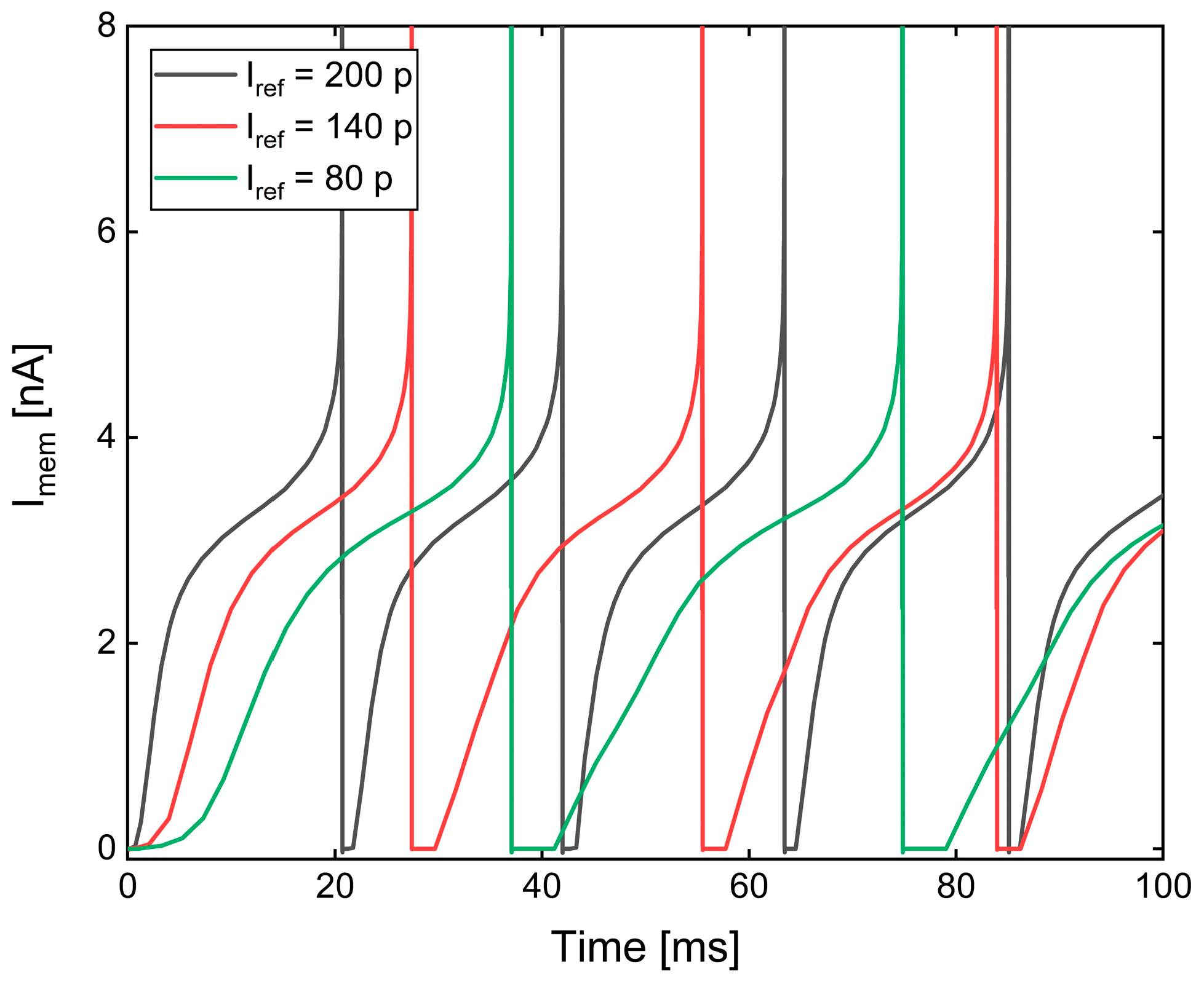
3.1. Neuron Circuit Post-Layout Simulation

Figure 8 shows LIF neural post-layout simulation results, exemplifying biologically plausible behaviors. It highlights distinct spiking patterns for a constant dc-current input, in contrast to the neuronal behavior described in [36]. In Figure 8, the input current for (a) to (e) was maintained at a constant value of 400 pA while, for (f), it varied linearly from 0 to 400 pA. The voltage values used to obtain spiking patterns are given in the figure description.
For a regular spiking (RS) pattern, the AHP module is currently closed and does not generate any leakage current for Cmem. The frequency adaptation (FA) spiking pattern allows Cadp to charge, causing the voltage Vahp to settle at a fixed value after a few spikes, resulting in slow-rate tonic spiking. The fast spiking (FS) pattern found in cortical layers is characterized by high-frequency periodic trains of spikes without adaptation, achieved by not allowing the membrane potential to reset all the way to the ground. Modulating the control voltage of K+ and AHP modules can manipulate tonic spiking (TS) and chattering (CH) spiking patterns. A tonic bursting neuron generates a burst of spikes at the beginning of a constant input current, followed by tonic spiking. A chattering neuron generates repetitive bursts of high-rate spikes in response to a constant input current. The neocortical RS excitatory neurons exhibit tonic spiking frequency that is proportional to the intensity of the input, ranging from 2 Hz to 200 Hz, or even higher. The property of firing low-frequency spikes at weak inputs is termed as Class 1 excitability [37]. These neurons can effectively represent the input strength through their firing rate, as depicted in Figure 8f.
The neuron biologically plausible behavior can be further verified. Figure 9 illustrates the behavior of neuronal refractory periods. The membrane current, Imem, was recorded at various Iref values by adjusting Vref in the K+ block of Figure 6. As Iref increases, the refractory period of the neuron is shorter and, hence, results in an increase in its maximum firing rate. This enables frequency modulation over a wide range in the neuron and exhibits significant potential for larger SNN systems [14,15,16,17]. The firing rate of neurons is the number of action potentials, or spikes, emitted over a defined time period, quantified in units of hertz (Hz) or spikes per second.
As previously stated, regulating the refractory period can shift the firing of neurons between high and low frequency modes. Due to the adjustable gate voltage feature of FDSOI devices, it is able to independently adjust the bias of the transistor MK2′s front-gate Vref and back-gate Vrefb. Figure 10 illustrates the FI curve of the neuron at varying bias levels of Vref and Vrefb. Specifically, Figure 10a,b show the FI curves in low-frequency and high-frequency modes,. When the back gate voltage, Vrefb, is set to ground, the resulting lower current, Iref, results in a longer refractory period and low frequency operation with the input current, until it reaches saturation at a level determined by the refractory period setting. Moreover, as Vref increases, the refractory period shortens, thereby increasing the neuron’s maximum firing rate. In addition, maintaining a proper fixed value for Vref and increasing the back-gate voltage Vrefb can lead to a shorter refractory period. As depicted in Figure 10b, as Vrefb increases, the firing rate of neurons also increases, operating at kilohertz levels. The maximum spiking firing rate is directly proportional to the input current and saturates only for extremely high input current values. When Vrefb reaches 300 mV, the refractory period is brief (a few hundred μs), and the maximum spike firing rate does not saturate, even for high input currents. This enables neurons to operate at higher frequencies as input current increases.
Figure 11 illustrates the spike frequency adaptation behavior. This was obtained by applying an input current step with an amplitude of 300 pA and a gain current (Igain) of 80 pA, with Vthrb = 0 V, Vleak = 60 mV, Vrep = 100 mV, Vref = 80 mV, Vpfb = −200 mV, Vadp = 25 mV, and Vadpb = 0 V. As each spike is generated, the adaptive after-hyperpolarization potential (Vahp) rises, leading to a corresponding increase in the adaptive current (Iahp) by MA2, which reduces the charging current of the membrane capacitance (Cmem). Once Vahp reaches a stable state, the spiking firing of the neuron remains constant, albeit at a lower rate compared to the initial firing. This process reduces the firing rate to lower energy consumption as a form of frequency adaptation.
In a large-scale spiking neural network, neurons are required to process information from multiple network layers. It is crucial for neurons to adapt the spiking information of varying frequencies at different network layers. Recent studies on mixed-signal neuromorphic systems [18,38] have suggested the use of wide-band adaptive neurons with time constants that are well-suited for signal processing. This neuron can also effectively achieve adaptive behavior at different frequencies, as illustrated in Figure 12. Adaptive frequencies can vary by adjusting the proportion between currents Ipf and Iadp. As can be seen, as the ratio of Ipf to Iadp increases, the adaptive spiking frequency also rises. Hence, the neuron is adept at implementing complex neuromorphic systems.

3.2. Energy Per Spike

It has been demonstrated that the proposed neural circuit exhibits sophisticated biologically resembling behavior. In order to evaluate its energy efficiency, energy consumption per spike is a significant figure of merit (FoM), and the FoM has been utilized in several studies to effectively assess the energy efficiency of neuron circuits [39,40,41,42]. Energy per spike can be calculated by dividing the average power consumption Pave by the maximum spiking frequency Freq. Averaged power is given by Equation (9):
P a v e = F r e q N 0 T s i m I d d t V d d d t
where Tsim is the simulation time, Idd (t) represents the total (static and dynamic) current flowing through the supply voltage Vdd, and N indicates the number of spikes in the simulation time Tsim. The energy per spike, denoted by ES, is extracted from Equation (9) and expressed as follows:
E S = P a v e F r e q = 1 N 0 T s i m I d d t V d d d t
Figure 13 demonstrates the energy per spike versus firing rate curve of the neuron. It is apparent that the low-frequency mode consumes more energy than the high-frequency mode. Energy consumption for lower frequencies is around tens of pJ, decreasing to hundreds of fJ for higher frequencies. This is because, at lower frequencies, the inverters operate in high-gain regions where both transistors conduct for longer periods, and this occurs due to slower charging of Vmem compared to higher frequencies. Furthermore, static power consumption when operating at 30 Hz represents about 11% of total power consumption, while, at higher frequencies (i.e., at 1 kHz), this percentage drops to 5%. Table 2 presents a comparison of the energy per spike of our circuit with previously published state-of-the-art neuron circuits. The simulation results of our neuron circuit are compared with both simulation data [41,42] and experimental data [32].
Compared to a similar 28 nm CMOS circuit [32], our design exhibits superior energy efficiency with energy consumption per spike at approximately 326 fJ at 1 kHz, which is three orders of magnitude lower than the firing rate of 1 kHz observed in the reference neuron. The neuron developed in this study consumes less energy per spike than a comparable circuit [41] using similar technology (28 nm FDSOI) at a biologically plausible spiking rate (30 Hz), and the circuits utilized in [41] and our study share comparable Cmem, which we can regard as the dominant capacitance impacting power consumption. Thus, based on the scaling factor, the circuit in [41] is expected to have comparable energy per spike when scaled down to the 22 nm process. Our circuit has a larger area than the circuit in [41], as the circuit includes an adaptive capacitor (Cadp) for enabling complex neural behaviors and a wide range of adjustable frequencies. Additionally, the capacitance density of 22 nm FDSOI devices exceeds that of 28 nm FDSOI devices with equivalent value, leading to a high capacitance utilization in the circuit area. Furthermore, the circuits proposed in both [42] and our study used the same technology (22 nm FDSOI). It can be noted that our circuit design offers greater efficiency in terms of area and energy consumption.

3.3. Monte Carlo Analysis

The proposed circuit is adaptable and can be flexibly controlled through parameter adjustments in various situations. However, process variability and mismatch cause device conducting currents that deviate from the intended values. If the mismatch is excessive, the output of neurons in a spiking neural network will exhibit significant variability from one neuron to another. To minimize transistor mismatch effects, we selected those that operate with small currents and assigned them longer length values (e.g., LPMOS = 28 nm, LNMOS = 32 nm). Key transistors relevant to mismatch, such as MA1 and MK2, were designated even larger sizes, up to 36 nm/4 μm. To evaluate the neuron’s performance in relation to mismatches, we conducted a series of Monte Carlo simulations. The neuron circuit performed analysis with 500 runs, with a dc-current being injected into the DIP block depicted in Figure 6, while the bias currents were adjusted to obtain a firing rate of approximately 67.1 Hz.
As depicted in Figure 14, the Monte Carlo distribution results demonstrate that the average firing rate of neurons is around the expected value (≈67.1 Hz), with a standard deviation of 2.026. Consequently, the variability in the neuron circuit amounts to 3.02% (Std Dev/Mean). Our analysis revealed that the variability is modulated by Na+ inhibition, specifically, MN2 and MN5. The circuits in the DIP and K+ blocks (as shown in Figure 6) are also sensitive to mismatches, especially with respect to ML1 and ML2 for the DIP block, and MK2 for the K+ block.

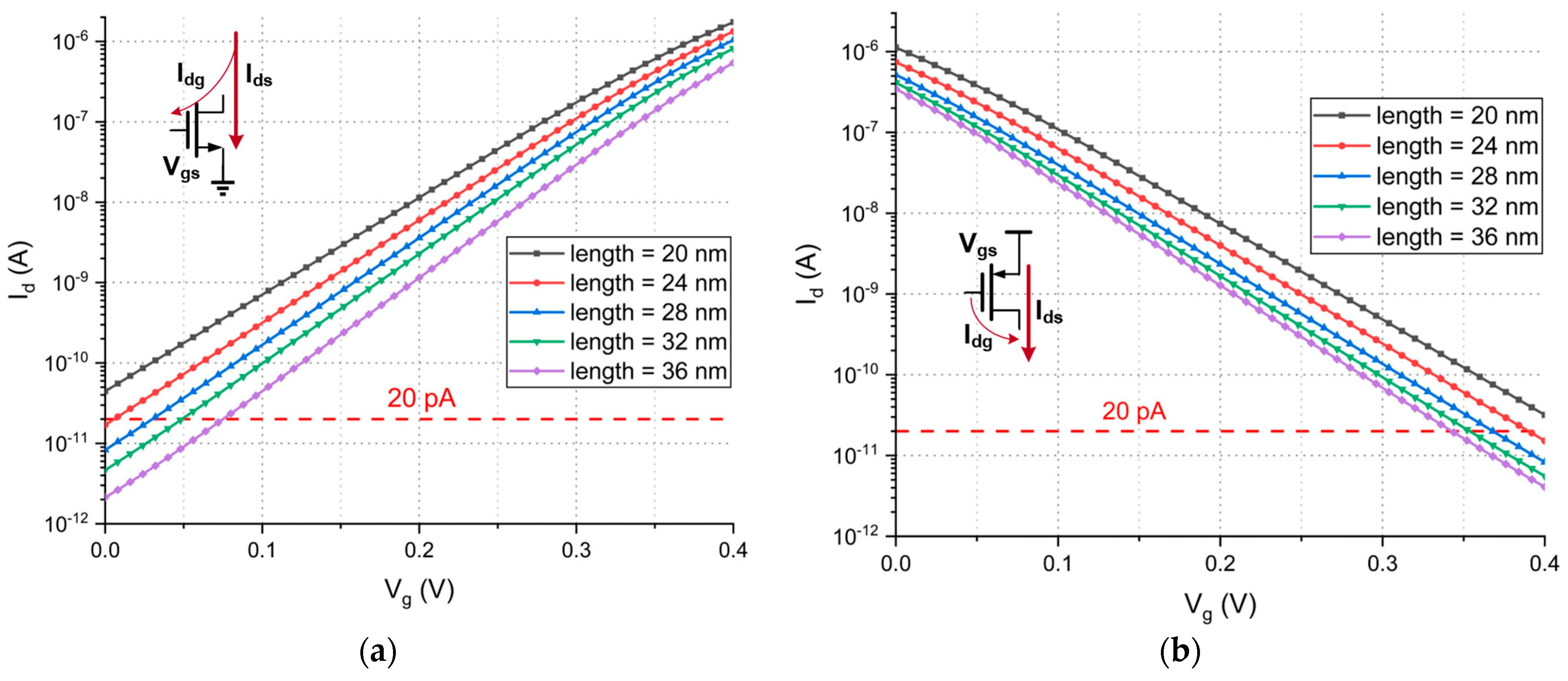
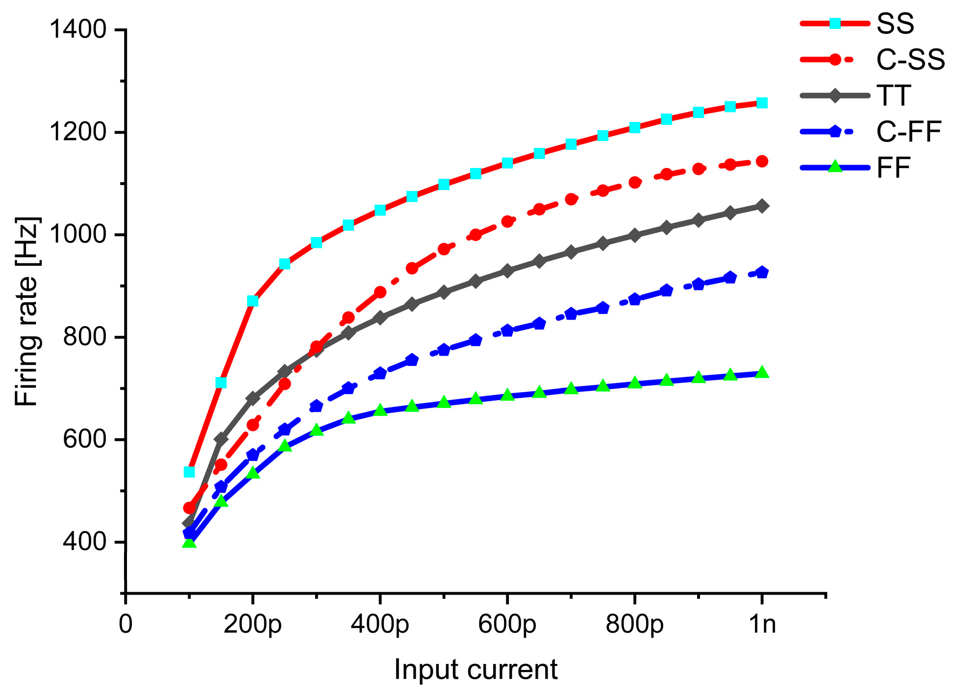
3.4. Process Robustness

Subthreshold neural circuits are highly sensitive to fluctuations in processing. In this FDSOI circuit design, we leveraged the advantages of back-gate voltage to regulate critical current paths and ensure robust process variation tolerance at extreme process corners, such as FF and SS.
Figure 15 illustrates the process variation for SS, TT, and FF. Specifically, the C–SS and C–FF curves were obtained by adjusting the transconductance between MN5, MK2, and MA1 at the corresponding process corners for SS and FF. It is evident that optimizing the back-gate voltage of key transistors improves the circuit’s robustness, and we can conclude that C–SS exhibits a 75.6% reduction in frequency deviation compared to TT, while C–FF experiences an 80.3% reduction relative to FF. As a result, the distinctions between C–SS and TT, as well as C–FF and TT, become negligible, suggesting that the proposed neural circuit can mitigate process variances.

4. Conclusions

We proposed a new efficient analog LIF neuron circuit, operating in the subthreshold regime, with ultra-low-power consumption and wide dynamics. It was implemented using an advanced 22 nm FDSOI process that had been scaled for optimal performance. A differential pair integrator circuit generated exponential subthreshold dynamics to accurately simulate the realistic time constant of neurons and synapses. The back-gate bias of FDSOI technology enables the generation of varied neuron dynamics over a wide frequency range, including low- and high-frequency modes, as well as adaptive frequencies. Moreover, this neuron is capable of displaying complex firing behaviors, such as adaptation, chattering, and bursting. These features render the suggested circuits well-suited for neuromorphic hardware systems. Compared to similar circuits, the proposed design exhibits lower energy consumption per spike, achieving 8.3 pJ at a 30 Hz firing rate. Monte Carlo simulations were performed to analyze the sensitivity of the neuron circuit to mismatches. Results indicate that the firing rate relative error is only 3.02% (Std Dev/Mean), highlighting the Na+ block, DPI block, and K+ block as the more sensitive sub-parts of the silicon neuron circuit. Finally, due to the significant transistor’s back-gate bias, this neuron exhibits higher process robustness across varying process corners.

Author Contributions

Conceptualization, study design, data analysis, data interpretation, and writing, J.Q.; Literature search and processing of graphics, J.Q. and Z.L.; resources, J.L.; writing—review and editing, B.L. and J.L. All authors have read and agreed to the published version of the manuscript.

Funding

This research received no external funding.

Data Availability Statement

Data used in this article will be made available on request to the corresponding author.

Conflicts of Interest

The authors declare no conflict of interest.

References

  1. Merolla, P.A.; Arthur, J.V.; Alvarez-Icaza, R.; Cassidy, A.S.; Sawada, J.; Akopyan, F.; Jackson, B.L.; Imam, N.; Guo, C.; Nakamura, Y.; et al. A million spiking-neuron integrated circuit with a scalable communication network and interface. Science 2014, 345, 668–673. [Google Scholar] [CrossRef]
  2. Sebastian, A.; Le Gallo, M.; Eleftheriou, E. Computational phase-change memory: Beyond von Neumann computing. J. Phys. D Appl. Phys. 2019, 52, 443002. [Google Scholar] [CrossRef]
  3. Grollier, J.; Querlioz, D.; Camsari, K.Y.; Everschor-Sitte, K.; Fukami, S.; Stiles, M.D. Neuromorphic spintronics. Nat. Electron. 2020, 3, 360–370. [Google Scholar] [CrossRef] [PubMed]
  4. Diehl, P.U.; Cook, M. Unsupervised learning of digit recognition using spike-timing-dependent plasticity. Front. Comput. Neurosci. 2015, 9, 99. [Google Scholar] [CrossRef] [Green Version]
  5. Lee, C.; Srinivasan, G.; Panda, P.; Roy, K. Deep spiking convolutional neural network trained with unsupervised spike-timing-dependent plasticity. IEEE Trans. Cogn. Dev. Syst. 2018, 11, 384–394. [Google Scholar] [CrossRef]
  6. Zhao, C.; Hamedani, K.; Li, J.; Yi, Y. Analog spike-timing- dependent resistive crossbar design for brain inspired computing. IEEE J. Emerg. Sel. Top. Circuits Syst. 2017, 8, 38–50. [Google Scholar] [CrossRef]
  7. Thakur, C.S.; Molin, J.L.; Cauwenberghs, G.; Indiveri, G.; Kumar, K.; Qiao, N.; Schemmel, J.; Wang, R.; Chicca, E.; Hasler, J.O.; et al. Large-scale neuromorphic spiking array processors: A quest to mimic the brain. Front. Neurosci. 2018, 12, 891. [Google Scholar] [CrossRef]
  8. Wu, X.; Saxena, V.; Zhu, K. Homogeneous spiking neuromorphic system for real-world pattern recognition. IEEE J. Emerg. Sel. Top. Circuits Syst. 2015, 5, 254–266. [Google Scholar] [CrossRef] [Green Version]
  9. Indiveri, G.; Corradi, F.; Qiao, N. Neuromorphic architectures for spiking deep neural networks. In Proceedings of the Electron Devices Meeting (IEDM), 2015 IEEE International. IEEE, Washington, DC, USA, 7–9 December 2015; pp. 4.2.1–4.2.14. [Google Scholar] [CrossRef]
  10. Wijekoon, J.H.B.; Dudek, P. Spiking and bursting firing patterns of a compact VLSI cortical neuron circuit. In Proceedings of the 2007 International Joint Conference on Neural Networks, Orlando, FL, USA, 12–17 August 2007; pp. 1332–1337. [Google Scholar] [CrossRef]
  11. Papadimitriou, K.I.; Eliu, S.-C.; Eindiveri, G.; Drakakis, E.M. Neuromorphic log-domain silicon synapse circuits obey Bernoulli dynamics: A unifying tutorial analysis. Front. Neurosci. 2015, 8, 428. [Google Scholar] [CrossRef] [Green Version]
  12. Frenkel, C.; Legat, J.-D.; Bol, D. A compact phenomenological digital neuron implementing the 20 Izhikevich behaviors. In Proceedings of the 2017 IEEE Biomedical Circuits and Systems Conference, Turin, Italy, 19–21 October 2017; pp. 1–4. [Google Scholar] [CrossRef]
  13. Indiveri, G.; Stefanini, F.; Chicca, E. Spike-based learning with a generalized integrate and fire silicon neuron. In Proceedings of the 2010 IEEE International Symposium on Circuits and Systems, Paris, France, 30 May–2 June 2010; pp. 1951–1954. [Google Scholar] [CrossRef] [Green Version]
  14. Qiao, N.; Mostafa, H.; Corradi, F.; Osswald, M.; Stefanini, F.; Sumislawska, D.; Indiveri, G. A reconfigurable on-line learning spiking neuromorphic processor comprising 256 neurons and 128K synapses. Front. Neurosci. 2015, 9, 141. [Google Scholar] [CrossRef] [Green Version]
  15. Furber, S.B.; Galluppi, F.; Temple, S.; Plana, L.A. The SpiNNaker Project. Proc. IEEE 2014, 102, 652–665. [Google Scholar] [CrossRef]
  16. Akopyan, F.; Sawada, J.; Cassidy, A.; Alvarez-Icaza, R.; Arthur, J.; Merolla, P.; Imam, N.; Nakamura, Y.; Datta, P.; Nam, G.-J.; et al. TrueNorth: Design and Tool Flow of a 65 mW 1 Million Neuron Programmable Neurosynaptic Chip. IEEE Trans. Comput. Aided Des. Integr. Circuits Syst. 2015, 34, 1537–1557. [Google Scholar] [CrossRef]
  17. Wu, X.; Saxena, V.; Zhu, K.; Balagopal, S. A CMOS spiking neuron for brain-inspired neural networks with resistive synapses and in situ learning. IEEE Trans. Circuits Syst. II Exp. Briefs 2015, 62, 1088–1092. [Google Scholar] [CrossRef] [Green Version]
  18. Kuang, Y.; Cui, X.; Zhong, Y.; Liu, K.; Zou, C.; Dai, Z.; Wang, Y.; Yu, D.; Huang, R. A 64K-neuron 64M-1b-synapse 2.64pJ/SOP neuromorphic chip with all memory on chip for spike-based models in 65nm CMOS. IEEE Trans. Circuits Syst. II Express Briefs 2021, 68, 2655–2659. [Google Scholar] [CrossRef]
  19. Cruz-Albrecht, J.M.; Yung, M.W.; Srinivasa, N. Energy-efcient neuron, synapse and STDP integrated circuits. IEEE Trans. Biomed. Circuits Syst. 2012, 6, 246–256. [Google Scholar] [CrossRef]
  20. Nakada, K.; Asai, T.; Amemiya, Y. Analog CMOS implementation of a bursting oscillator with depressing synapse. In Proceedings of the 2004 Intelligent Sensors, Sensor Networks and Information Processing Conference, Melbourne, Australia, 14–17 December 2004; pp. 503–506. [Google Scholar] [CrossRef]
  21. Lee, Y.J.; Lee, J.; Kim, Y.; Ayers, J.; Volkovskii, A.; Selverston, A.; Abarbanel, H.; Rabinovich, M. Low power real time electronic neuron VLSI design using subthreshold technique. In Proceedings of the 2004 IEEE International Symposium on Circuits and Systems, Vancouver, BC, Canada, 23–26 May 2004; Volume 4, pp. 744–747. [Google Scholar] [CrossRef]
  22. Folowosele, F.; Etienne-Cummings, R.; Hamilton, T.J. A CMOS switched capacitor implementation of the Mihalas-Niebur neuron. In Proceedings of the 2009 IEEE Biomedical Circuits and Systems Conference, Beijing, China, 26–28 November 2009; pp. 105–108. [Google Scholar] [CrossRef]
  23. Izhikevich, E.M. Simple model of spiking neurons. IEEE Trans. Neural Netw. 2003, 14, 1569–1572. [Google Scholar] [CrossRef] [Green Version]
  24. Chicca, E.; Stefanini, F.; Bartolozzi, C.; Indiveri, G. Neuromorphic electronic circuits for building autonomous cognitive systems. Proc. IEEE 2014, 102, 1367–1388. [Google Scholar] [CrossRef] [Green Version]
  25. Livi, P.; Indiveri, G. A current-mode conductance-based silicon neuron for address-event neuromorphic systems. In Proceedings of the 2009 IEEE International Symposium on Circuits and Systems, Taipei, Taiwan, 24–27 May 2009; pp. 2898–2901. [Google Scholar] [CrossRef] [Green Version]
  26. van Schaik, A.; Jin, C.; McEwan, A.; Hamilton, T.J. A log- domain implementation of the Izhikevich neuron model. In Proceedings of the 2010 IEEE International Symposium on Circuits and Systems, Paris, France, 30 May–2 June 2010; pp. 4253–4256. [Google Scholar] [CrossRef]
  27. Bartolozzi, C.; Mitra, S.; Indiveri, G. An ultra-low power current- mode filter for neuromorphic systems and biomedical signal processing. In Proceedings of the 2006 IEEE Biomedical Circuits and Systems Conference, London, UK, 29 November–1 December 2006; pp. 130–133. [Google Scholar] [CrossRef]
  28. Bee, X.E.; Fauzi, M.M.B.M.; Tan, P.B.Y. Modeling of MOSFET subthreshold swing mismatch with BSIM4 Model. In Proceedings of the IEEE International Conference on Semiconductor Electronics (ICSE), Kuala Lumpur, Malaysia, 17–19 August 2016; Volume 6, pp. 86–88. [Google Scholar] [CrossRef]
  29. Rajasekharan, D.; Kushwaha, P.; Chauhan, S.S.; Chauhan, Y.S. Non-boolean associative processing using FDSOI MOSFET-based inverter. IEEE Trans. Nanotechnol. 2018, 17, 1235–1243. [Google Scholar] [CrossRef]
  30. Carbon, A.; Philippe, J.-M.; Bichler, O.; Schmit, R.; Tain, B.; Briand, D.; Ventroux, N.; Paindavoine, M.; Brousse, O. PNeuro: A scalable energy-efficient programmable hardware accelerator for neural networks. In Proceedings of the 2018 Design, Automation & Test in Europe Conference & Exhibition, Dresden, Germany, 19–23 March 2018; pp. 1039–1044. [Google Scholar] [CrossRef]
  31. Schemmel, J.; Kriener, L.; Muller, P.; Meier, K. An accelerated analog neuromorphic hardware system emulating NMDA- and calcium-based non-linear dendrites. In Proceedings of the 2017 International Joint Conference on Neural Networks (IJCNN), Anchorage, AK, USA, 14–19 May 2017; pp. 2217–2226. [Google Scholar] [CrossRef] [Green Version]
  32. Mayr, C.; Partzsch, J.; Noack, M.; Hanzsche, S.; Scholze, S.; Hoppner, S.; Ellguth, G.; Schuffny, R. A biological-realtime neuromorphic system in 28 nm CMOS using low-leakage switched capacitor circuits. IEEE Trans. Biomed. Circuits Syst. 2016, 10, 243–254. [Google Scholar] [CrossRef] [PubMed] [Green Version]
  33. Folowosele, F.; Harrison, A.; Cassidy, A.; Andreou, A.G.; Etienne-Cummings, R.; Mihalas, S.; Niebur, E.; Hamilton, T.J. A switched capacitor implementation of the generalized linear integrate-and-fire neuron. In Proceedings of the 2009 IEEE International Symposium on Circuits and Systems, Taipei, Taiwan, 24–27 May 2009; pp. 2149–2152. [Google Scholar] [CrossRef]
  34. Bellec, G.; Salaj, D.; Subramoney, A.; Legenstein, R.; Maass, W. Long short-term memory and learning-to-learn in networks of spiking neurons. Adv. Neural Inf. Process. Syst. 2018, 31, 787–797. [Google Scholar]
  35. Le Guevel, L.; Billiot, G.; Paz, B.C.; Tagliaferri, M.L.V.; De Franceschi, S.; Maurand, R.; Cassé, M.; Zurita, M.; Sanquer, M.; Vinet, M.; et al. Low-power transimpedance amplifier for cryogenic integration with quantum devices. Appl. Phys. Rev. 2020, 7, 041407. [Google Scholar] [CrossRef]
  36. Izhikevich, E.M. Which model to use for cortical spiking neurons? IEEE Trans. Neural Netw. 2004, 15, 1063–1070. [Google Scholar] [CrossRef]
  37. Chicca, E.; Indiveri, G. A recipe for creating ideal hybrid memristive-CMOS neuromorphic processing systems. Appl. Phys. Lett. 2020, 116, 120501. [Google Scholar] [CrossRef]
  38. Frenkel, C.; Lefebvre, M.; Legat, J.-D.; Bol, D. A 0.086-mm2 12.7-pJ/sop 64k-synapse 256-neuron online-learning digital spiking neuromorphic processor in 28-nm CMOS. IEEE Trans. Biomed. Circuits Syst. 2019, 13, 145–158. [Google Scholar] [CrossRef] [PubMed] [Green Version]
  39. Bédécarrats, T.; Fenouillet-Béranger, C.; Cristoloveanu, S.; Galy, P. A BIMOS-based 2T1C analogue spiking neuron circuit integrated in 28 nm FD-SOI technology for neuromorphic application. Solid-State Electron. 2020, 168, 107717. [Google Scholar] [CrossRef]
  40. Cincon, V.; Vatajelu, E.I.; Anghel, L.; Galy, P. From 1.8V to 0.19V voltage bias on analog spiking neuron in 28nm UTBB FDSOI technology. In Proceedings of the 2020 Joint International EUROSOI Workshop and International Conference on Ultimate Integration on Silicon, Caen, France, 1–30 September 2020; pp. 1–4. [Google Scholar] [CrossRef]
  41. Qiao, N.; Indiveri, G. Scaling mixed-signal neuromorphic processors to 28 nm FD-SOI technologies. In Proceedings of the 2016 IEEE Biomedical Circuits and Systems Conference, Shanghai, China, 17–19 October 2016; pp. 55–555. [Google Scholar] [CrossRef] [Green Version]
  42. Rubino, A.; Livanelioglu, C.; Qiao, N.; Payvand, M.; Indiveri, G. Ultra-low-power FDSOI neural circuits for extreme-edge neuromorphic intelligence. IEEE Trans. Circuits Syst. I Regul. Pap. 2021, 68, 45–56. [Google Scholar] [CrossRef]
Figure 1. FDSOI device structure.
Electronics 12 02648 g001
Figure 2. Simulated subthreshold IdVg characteristics are shown for LVT NMOS (a) and PMOS (b) transistors with different channel lengths, under the condition of |Vds| = 400 mV and W = 1 µm.
Electronics 12 02648 g002
Figure 3. IdVg characteristics of two LVT NMOS and PMOS devices, with the same channel width W = 400 nm, as functions of their back-gate bias.
Electronics 12 02648 g003
Figure 4. Example of LIF neuron model.
Electronics 12 02648 g004
Figure 5. Proposed method.
Electronics 12 02648 g005
Figure 6. Proposed subthreshold neuron circuit schematic.
Electronics 12 02648 g006
Figure 7. Layout of the proposed neuron circuit.
Electronics 12 02648 g007
Figure 8. Different spiking patterns from the LIF neuron. For all cases Vdd = 400 mV, Vthrb = − 400 mV, Vleak = 90 mV, Vadpb = 0 V. (a) RS: Vrep = 120 mV, Vref = 80 mV, Vpfb = 400 mV, Vadp = 5 mV; (b) FA: Vrep = 80 mV, Vref = 80 mV, Vpfb = −200 mV, Vadp = 25 mV; (c) FS: Vrep = 90 mV, Vref = 120 mV, Vpfb = 400 mV, Vadp = 5 mV; (d) TS: Vrep = 80 mV, Vref = 80 mV, Vpfb = 150 mV, Vadp = 5 mV; (e) CH: Vrep = 150 mV, Vref = 100 mV, Vpfb = 100 mV, Vadp = 35 mV; (f) Class 1 excitable: Vrep = 150 mV, Vref = 100 mV, Vpfb = 80 mV, Vadp = 25 mV.
Electronics 12 02648 g008
Figure 9. Membrane current Imem for different values of Iref.
Electronics 12 02648 g009
Figure 10. Firing rate vs. input current (FI) curve (a) for low-frequency mode with longer refractory period, (b) for high-frequency mode with shorter refractory period.
Electronics 12 02648 g010
Figure 11. Frequency adaptation: membrane and after-hyperpolarization voltage trace over time.
Electronics 12 02648 g011
Figure 12. Neuron adaptive behavior at different frequencies.
Electronics 12 02648 g012
Figure 13. Energy per spike estimation: energy per spike vs. firing rate in (a) low-frequency mode, (b) high-frequency mode.
Electronics 12 02648 g013
Figure 14. Monte Carlo analysis result distribution.
Electronics 12 02648 g014
Figure 15. Firing rate vs. input current (FI) curve in different process corners.
Electronics 12 02648 g015
Table 1. Capacitance values and sizes used in the neuron design.
CmemCrefCadp
Value383 fF227 fF639 fF
Width9 µm9 µm15.5 µm
Length12 µm7 µm18 µm
Table 2. The proposed circuit in comparison with other works.
Work[32][41][42]This Work
Techn.28 nm CMOS28 nm FDSOI22 nm FDSOI22 nm FDSOI
Vdd0.7–1 V1 V0.8 V0.4 V
Area-20 μm2900 μm2484 μm2
ResultsExpSimSimSim
En./spike2.3nJ@1kHz50pJ@30Hz14pJ@30Hz326fJ@1kHz
8.3pJ@30Hz
Disclaimer/Publisher’s Note: The statements, opinions and data contained in all publications are solely those of the individual author(s) and contributor(s) and not of MDPI and/or the editor(s). MDPI and/or the editor(s) disclaim responsibility for any injury to people or property resulting from any ideas, methods, instructions or products referred to in the content.

