Abstract
A deep neural network (DNN)-based method is proposed for the fast synthesis of a high-dimensional electromagnetic bandgap structure (HD-EBG) suppressing the power/ground noise in high-speed packages and printed circuit boards (PCBs). In recent EBG structures, a highly flexible design with high dimensionality is required, which is challenging to rapidly achieve an optimal solution. The proposed synthesis method is developed to solve this issue efficiently. The DNN hyperparameter optimization (HPO) associated with the HD-EBG structure is devised using the orthogonal array of the Taguchi method. By using this approach, the search space for HPO is reduced. For the efficient synthesis of the HD-EBG structure, an inverse modeling approach based on a DNN forward model and genetic algorithm optimization is proposed. The proposed DNN inverse modeling (DIM) is applied to two design examples where the HD-EBG structures with a constant fractional bandwidth and stopband bandwidth extension are synthesized. In the demonstration cases, the proposed DIM achieves the fast and accurate synthesis of the HD-EBG structures compared to the conventional method. With the proposed method, the synthesis time is maximally reduced up to 99.8% compared to conventional synthesis based on the forward model of full-wave simulation.
1. Introduction
Power/ground noise in microwave and high-speed digital circuits has received substantial attention in recent years. The suppression of high-frequency power/ground noise in high-speed packages and printed circuit boards (PCBs) is necessary to achieve high performance and reliability in high-speed digital and microwave systems. An electromagnetic bandgap structure (EBG) has been introduced as an effective way to mitigate high-frequency power/ground noise in high-speed packages and PCBs.
The overall performances and benefits of EBG structures are comprehensively summarized in [1]. The mushroom-type and coplanar EBG structures are revisited, and their noise suppression characteristics and dispersion analysis are explained, providing insight into the EBG structure for a better understanding. In [2], the initial study of the mushroom-type EBG structure was presented to suppress parallel-plate noise in power/ground planes. To improve the mushroom-type EBG structure, high-dielectric constant material was employed in [3]. Embedded capacitance material is placed between the power and ground planes of the EBG structure. The effective capacitance increases without enlarging the size of the EBG structure. This results in a wideband stopband with miniaturization. However, the use of high-dielectric constant materials in the EBG structure poses challenges such as high manufacturing costs and reduced reliability. To overcome this problem, a technique based on a defected ground structure (DGS) was presented in [4,5,6]. The implementation of the DGS is simple and cost-effective, as it involves etching copper in a metal layer during the manufacturing process. Various-shaped DGS patterns were applied to the metal plane connecting with an EBG patch to improve the stopband of the EBG structure. The rectangular-shaped DGS in [4] substantially broadens the stopband bandwidth by increasing the high cutoff frequency. The circular-shaped DGS is presented in [5] to improve a stopband with a reduced DGS area. Although rectangular- and circular-shaped DGSs improve the stopband of the EBG structure, they mainly increase the high cutoff frequency of the stopband rather than reduce the low cutoff frequency. In [6], a spiral-shaped pattern is devised for decreasing the low cutoff frequency of a stopband, leading to the miniaturization of the EBG structure. The compact EBG structure is beneficial for the implementation of noise suppression filters in integrated circuit packages. In [2,3,4,5,6], EBG structures require a significant amount of space to form a periodic structure. To reduce the occupied area, researchers have proposed a technique that partially employs the EBG structure [7]. This approach provides a trade-off solution between the stopband characteristics and the areas of the EBG structure on the board.
The coplanar EBG structure is another prominent type of EBG structure. It has been utilized to suppress the power/ground noise in high-speed circuits, as demonstrated in [8]. The structure comprises a stepped impedance resonator with both high and low characteristic impedances, which can be achieved by etching copper on the power or ground plane. The EBG structure described in [8] achieves a stopband in a simple manner; however, its ability to suppress power/ground noise over the wideband frequency range is limited. Therefore, an embedded thin film with a high-dielectric constant material is adopted, as demonstrated in [9,10]. The use of a high-dielectric constant material increases the capacitance of each EBG unit cell, resulting in efficiently broadening a stopband. However, due to the difficulty in handling the embedded thin film sheet and its low reliability, implementing this technique in manufacturing remains a significant challenge. To address this issue, the use of a rod-shaped structure made of a high-dielectric constant material is presented in [11], which not only improves the stopband of the EBG structure but also ensures high reliability in the manufacturing process. As described in previous studies, EBG structures exhibit the advantages of wideband suppression, substrate integration, high rejection level, and various analysis methods.
Bandgap characteristics are among the critical factors of the performance of an EBG structure for power/ground noise suppression, namely, a stopband consisting of low and high cutoff frequencies (fL and fH). In the design of EBG applications, the primary objective is to form a stopband covering a target frequency range where the power/ground noise should be mitigated. Considering the various target frequencies of recent and emerging applications of EBG structures, the synthesis of an EBG structure covering a target frequency range is quite a challenging problem. To achieve this objective, the fL and fH of a stopband must be adjusted with a high degree of flexibility. Consequently, a high-dimensional EBG structure (HD-EBG) should be considered that includes more design parameters than conventional EBG structures. Thus, it implements a massive design space.
A large design space ensures the existence of proper values of the design parameters that form a stopband, satisfying a target frequency band. However, this increase challenges the search for an optimized value in a limited timeframe. Extracting a one-to-one mapping function between the geometric variables and cutoff frequencies is more challenging in an HD-EBG structure because of the high dimensionality induced by many variables. It is hindered in obtaining an analytical solution and constructing an inverse model for the fast synthesis of HD-EBG structures.
Numerical approaches have been introduced to overcome the challenges of inverse modeling [12,13,14]. In [12], a stepped impedance EBG structure was synthesized using the fL and fH equations based on cavity mode resonances. Since the fundamentals governing the EBG structure in [12] are simple, a closed-form expression for physical dimensions can be obtained. However, this approach is limited to an EBG structure with low dimensionality, and it is difficult to extend this to an HD-EBG structure.
In [13], a highly flexible approach was presented. This study combines an optimization technique based on a genetic algorithm (GA) and forward model constructed using electromagnetic simulation, such as the finite difference method (FDM). An arbitrary-shaped perforation was formed in a patch with low characteristic impedance. Therefore, high dimensionality was implemented for EBG synthesis. However, the coupling effect within the perforation pattern cannot be captured by FDM, resulting in an inaccurate prediction of fL and fH. Moreover, GA optimization based on FDM requires an extremely long computation time.
In [14], a full-wave simulation of the finite element method (FEM) was employed for the forward modeling of the HD-EBG structure. The FEM simulation sufficiently increased the flexibility of the structural design and the accuracy of the simulation results. To obtain the HD-EBG structure satisfying the target frequency band, an FEM simulation was repeated numerous times in the GA optimization. This iterative process requires a long time for EBG synthesis because each full-wave simulation requires a significant computation time. Although combining an optimization technique with a full-wave simulation is effective for inverse modeling, the synthesis time should be substantially reduced.
To minimize the synthesis time and overcome the challenges in inverse modeling of an HD-EBG structure, a synthesis method based on a deep neural network (DNN) is proposed in this study. A DNN is defined as an artificial neural network consisting of many hidden layers. Recently, numerous studies on applying a DNN model to microwave and high-speed digital applications, such as microwave filters and high-speed interconnect systems, have been introduced. In [15,16,17], initial studies on the modeling of microwave circuits using artificial neural networks (ANNs) have been introduced. In the early stages of the study, researchers primarily focused on the computer-aided design of microwave circuits using the shallow neural network consisting of one or two hidden layers. ANN-based modeling achieves fast and accurate prediction of circuit performances and reduces the effort required for developing costly model libraries. To tackle the limitations imposed by a small number of hidden layers, the utilization of DNN is considered and the modeling method based on neural networks is extended to include more complex types of microwave circuits. In [18], the dynamic non-linearity of a wideband power amplifier is predicted using ANNs. The feedforward DNN is applied to microwave passive components such as a three-pole H-plane filter and a fifth-order waveguide bandpass filter in [19]. The mode recognition of dielectric resonator antenna is performed using a DNN technique to improve the antenna’s performance in [20]. The DNN-based approach has proven to be highly effective in modeling microwave circuits, and the researchers are additionally exploring the application of the DNN-based approach in a high-speed interconnect design in [21,22,23]. The design of the high-speed channel, including the analysis of eye diagrams, is effectively demonstrated with high accuracy and efficient computation. Moreover, the DNN-based approach in [24] finds application in the domain of power integrity design, specifically for utilizing the EBG structure to mitigate the power/ground noise in high-speed packages and PCBs. Clearly, the DNN-based method demonstrates notable features in modeling various microwave applications. However, the introduction of more input parameters and complicated network structures gives rise to the challenge of high dimensionality. This problem is extensively tackled in [25,26,27], where comprehensive solutions are provided.
In previous studies, DNN-based approaches have shown the ability to efficiently solve the inverse modeling problems of circuits with high dimensionality. However, relevant studies reporting the synthesis of HD-EBG structures using a DNN-based approach for power/ground noise suppression in high-speed packages and PCBs are challenging to find. Moreover, the hyperparameter optimization (HPO) of a DNN model dedicated to an HD-EBG structure is not observed, which is significant for achieving the fast and accurate synthesis of an HD-EBG structure.
The primary contribution of this study is the development and analysis of a dedicated DNN-based synthesis method for high-dimensional EBG structures, aiming to mitigate the power/ground noise in high-speed packages and PCBs. To ensure efficient synthesis, an effective approach for reducing the design space is devised using the Taguchi method. Additionally, an optimization method for the ANN structure is developed. The proposed method exhibits its remarkable capabilities compared to the conventional method, as demonstrated via full-wave simulations. In this study, a DNN-based synthesis method is proposed for the fast design of an HD-EBG structure that suppresses power/ground noise in high-speed packages and PCBs. A hybrid model of DNN and GA optimization for inverse modeling and an HPO method for reducing dimensionality are performed. Various HD-EBG structures were considered to verify and demonstrate the proposed synthesis method.
2. Proposed EBG Synthesis Method
2.1. Hybrid Model for Inverse Modeling
The proposed EBG synthesis method mainly consists of two parts: the Taguchi-method-based HPO (TM-HPO) and DNN-based inverse modeling (DIM), as shown in Figure 1. In both steps, the hybrid model containing the DNN forward model and GA optimization is adopted. The proposed hybrid model efficiently achieves an indirect inverse model for the HD-EBG structure. A DNN forward model is constructed, as shown in Figure 2. The input of the DNN model is the binary array s of the design parameters for an HD-EBG structure. The output is the array f of the low and high cutoff frequencies (fL and fH) expressed in decimals. The DNN model in the proposed EBG synthesis method contains fully connected layers comprising an input layer with Nb neurons, M hidden layers with NL(i) neurons, and an output layer with two neurons. The input array s is used as the binary-coded chromosome in the GA, and its size is denoted as Nb. k represents the kth run of the orthogonal array (OA) of Lj(Si) obtained via the Taguchi method, which is used in the TM-HPO. The Taguchi method is proposed for the robust design of engineering problems. By using the Taguchi method, experiment sets are given, which consist of a variety of design parameters that require investigation by changing them from one value to another. The results obtained from completing Taguchi experiments provide insight into the effects of various design parameters. This leads to the efficient design of complex problems suffering from extensive design space. Taguchi experiments are designed using an orthogonal array. The number of design variables and their levels determine the size of the orthogonal array. In this study, we employ the Taguchi method to efficiently reduce the design space. ELU is employed as an activation function. It enables one to avoid a vanishing gradient problem and improve learning characteristics [28].
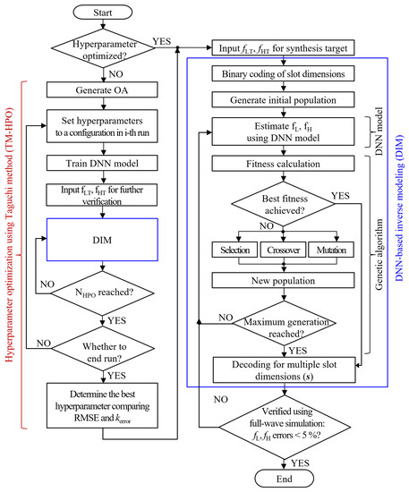
Figure 1.
Procedure of proposed method consisting of TM-HPO and DIM for fast synthesis of an EBG structure with high dimensionality.
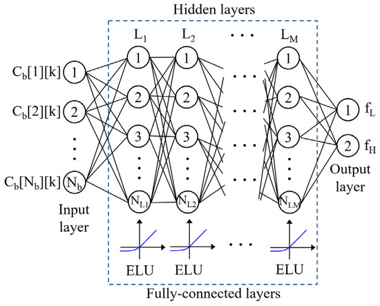
Figure 2.
DNN model and hyperparameters optimized using Taguchi orthogonal array in TM-HPO.
In addition to the DNN model, the GA was adopted in the proposed DIM. To explain this, a multi-slot patch EBG structure was employed as an example of an HD-EBG structure, as shown in Figure 3. The unit cell of the multi-slot EBG structure consisted of a power plane, ground plane, and perforated patch, where six different slots were etched. In the design of the HD-EBG structure, the values of the unit cell size dc, via radius rv and length hv, and the distance hc between the patch and the ground plane were employed. These variables are typically preferred not to change because they are constrained by the stack-up and layout of high-speed packages and boards. Consequently, the slot dimensions were determined as the primary design variables because they rarely affect stack-up and layout. The slot dimensions were width wsi and length Lsi of the ith slot. They were adjusted to obtain the EBG design satisfying the targets fL and fH, which are represented as fLT and fHT. The dimensions of the slots were encoded as a binary array, as shown in Figure 3, since the values of the input layer in the DNN model were updated using the optimization method based on the binary GA. The length of the input binary array was 54 bits. It consisted of six subarrays, where three and six bits were used to denote the width and length of each slot, respectively.
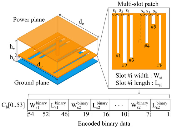
Figure 3.
Unit cell of an HD-EBG structure with main design variables of multiple slots and a binary chromosome for DNN input.
A binary array of slot dimensions for the DNN input layer was randomly generated and used as the initial population of the GA. The population consisted of 1000 chromosomes. To generate offspring, 30% of chromosomes from parents with lower error values were selected in the selection step. In a crossover step, the cross points were 1, 4, 10, 13, 19, 22, 28, 31, 37, 40, 48, and 54 bits. A bit flip with 50% probability was employed in the mutation step. The GA was repeated until the iteration reached the maximum number of 1000.
The GA objective is to minimize the fitness of the error between fLD and fHD, estimated via the DNN model, and target fLT and fHT, as follows:
At the end of the GA, the optimal estimation for slot dimensions s* was acquired.
2.2. TM-HPO and DIM
The TM-HPO was performed to obtain the best configuration of the DNN model and increase the accuracy of the hybrid model. In the proposed method, the Taguchi method was adopted to optimize the architecture of a neural network by reducing the search space for the HPO. In general, acquiring an optimized set of hyperparameters depends considerably on the researcher’s experience. Moreover, this is a time-consuming process due to the huge search space. The Taguchi method lowers the technological threshold of initializing the HPO and reduces the effort of searching for the hyperparameters to achieve maximum accuracy. The search space is determined based on the OA of the Taguchi method. Consider that the HPO variables consist of i factors with S levels, and Si cases should be considered in a full factorial approach. The Taguchi method yields only j cases to be considered, based on the OA of Lj(Si), which substantially reduces the number of cases to be considered. Although OA cases do not ensure a global optimum in certain cases, they provide a reasonable solution and enable a systematic approach.
In the proposed synthesis method, four hyperparameters of (1) a neural network structure, (2) the number of neurons in a hidden layer, (3) the number of hidden layers, and (4) the learning rate (LR) were selected as variables for HPO since they significantly affect the DNN model accuracy and computation time. Regarding the first hyperparameter, a neural network structure employs three alternatives which comprise the different neuron numbers in the hidden layers. The first configuration, C1, is a neural network with a constant number of neurons in each hidden layer. The other DNN network structures exhibit a linear decrease C2 and stepped decrease C3. The DNN configuration is represented as follows:
The second hyperparameter to be considered was the number of neurons in the first hidden layer NL1. Three values of 54, 64, and 74 were employed for NL1 in TM-HPO. Third, the hidden layer numbers M were selected as 4, 8, and 16. The last hyperparameter to be considered was LRs, which are closely associated with model training. Their values were 0.001, 0.005, and 0.01. The factors and corresponding levels for the TM-HPO are summarized in Table 1. The factors and levels yielded an OA of L9(34), as shown in Table 2. The OA consisted of nine runs. The search space for HPO was substantially reduced compared to the full factorial design. For every run in OA, DNN model training and validation were, respectively, performed under the corresponding hyperparameter configurations.

Table 1.
Design variables and their levels for TM-HPO.
Table 2.
Orthogonal array for TM-HPO.
Afterward, we completed the training and validation of the DNN model under the condition of each run in the OA. Furthermore, verification was performed to reduce the error in the DNN model. The target fLT,HPO and fHT,HPO were selected for additional verification of the DNN model. The trained DNN model constructed an aforementioned hybrid model that provided the optimal slot dimensions for the synthesis of the EBG structure with fLT,HPO and fHT,HPO. i represents the ith run of OA. Dispersion analysis of the HD-EBG structure according to was conducted using a full-wave simulation in the further verification step. The cutoff frequencies of the HD-EBG structure with slot dimensions were obtained, and they are denoted as and . For comprehensive analysis, the EBG synthesis under the conditions of the same fLT,HPO and fHT,HPO was repeated NHPO times. Afterward, the number of obtained values of and was NHPO. For the ith run of the OA, the accuracy was judged by the values of the root mean square error (RMSE), as follows:
Finally, the best hyperparameters were determined by comparing the error values of all runs, as shown in (4). The optimal hyperparameters were employed in the hybrid model of DIM, which was primarily used for EBG synthesis. With these best hyperparameters, the HD-EBG structures were synthesized in the DIM part, as shown in Figure 1. DIM mainly contains two steps: the DNN-GA hybrid model and further verification based on the dispersion analysis with full-wave simulation. The DNN-GA hybrid model yielded the optimal values of the slot dimensions for the given objectives of fLT and fHT. In the further verification step of DIM, fLE and fHE were acquired by conducting dispersion analysis with the full-wave simulation of the HD-EBG structure corresponding to . Although the optimal hyperparameters were extracted in TM-HPO, errors between the target values (i.e., fLT and fHT) and the synthesis results (i.e., fLE and fHE) can exist due to the uncertainty of the DNN model. This problem was solved by employing a further verification step using a full-wave simulation. This led to an increase in the synthesis time. However, the time increase was quite small compared to a conventional method, which fully adopts full-wave simulation as a forward model. In the further verification step, the DIM step was repeated NDIM times until the errors of both fLE and fHE reached <5%. Afterward, the final solution of the slot dimensions for the HD-EBG structure was obtained.
3. Results of HD-EBG Synthesis
3.1. DNN Model and TM-HPO
To verify and demonstrate the proposed synthesis method, two design cases, a constant fractional bandwidth (FBW) and stopband extension, were considered in DIM. Prior to performing the design cases implemented by DIM, the TM-HPO should be completed for both design cases. In this subsection, DNN model training, validation, and TM-HPO are explained, and design cases are described in the following subsections.
The specific dimensions of the HD-EBG structure were considered, as listed in Table 3, and were used in the design cases. The unit cell length dc and patch length dp were 5.2 mm and 5.0 mm, respectively. Both radius rv and length hv were 0.2 mm. The distance hc between the patch and ground plane was 0.1 mm. The slot widths for the six slots varied from 0.1 to 0.5 mm, while the slot lengths changed from 0.1 to 4.8 mm. As described in Section 2, the width and length of each slot were encoded into 3- and 6-bit binary values in a binary slot dimension array . The step values for the width and lengths were 0.4/7 and 4.7/63 mm (i.e., approximately 0.057 and 0.075 mm), respectively. These variations in the slots were applied to both dataset generation for a DNN model used in TM-HPO and DIM.
Table 3.
Design parameters and dimensions of HD-EBG structure in Figure 3.
Regarding the datasets for the training and validation of a DNN model, the datasets were obtained using 1D dispersion analysis and a full-wave simulation of various slot dimensions. Furthermore, 4212 and 1052 simulation results were acquired for the training and validation of the DNN model, respectively. The relationship between fL and fH for the datasets is shown in Figure 4. As shown in the datasets, the design space of the HD-EBG structure is not a simple linear curve. It exhibits multiple solutions that reflect its ability to tune cutoff frequencies and its non-unique characteristics.
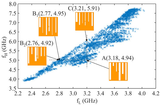
Figure 4.
Design space of cutoff frequencies (fL and fH) with various slot dimensions for training and validation dataset of a DNN model.
For tunability, an independent adjustment between fL and fH can be achieved by selecting alternative dimensions. For example, suppose that the HD-EBG structure (i.e., test vehicle (TV) A) is initially designed to have an fL of 3.18 GHz and fH of 4.94 GHz, and its fL needs to be lowered to 2.8 GHz whilst maintaining fH. Subsequently, the slot dimensions must be redesigned. Selecting the slot dimensions corresponding to TV B1 in Table 4 enables us to obtain the HD-EBG structure with an fL of 2.77 GHz and fH of 4.95 GHz, which shows the fL reduction with a similar fH. Moreover, a solution exists for this issue. Additionally, selecting the slot dimensions corresponding to TV B2 in Table 4 can yield a similar result. It is shown that multiple solutions exist in the design of the HD-EBG structure due to the non-unique characteristics of the HD-EBG design.
Table 4.
Design parameters and dimensions of HD-EBG structure in Figure 4.
Considering the other scenario, we assume that the fH of TV A should be increased without changing fL. The initial design of TV A can be replaced by the design of TV C. As shown in Figure 4, fH is extended from 4.94 (TV A) to 5.91 GHz (TV C), while the fL values of TV A and C are approximately the same. Therefore, the design of the fH extension without changing fL is achieved. We observed from the two scenarios that an EBG structure with high dimensionality has the advantage of enabling a flexible design that is challenging to achieve in a low-dimensional EBG structure. However, high dimensionality and non-uniqueness lead to conflicts between flexible design and inverse modeling. This contradictory issue is solved using the proposed synthesis method as described in Section 2.
Now, the TM-HPO was applied and the results were obtained. The OA values are presented in Table 2. For further verification, the values of fLT,HPO and fHT,HPO were set to 3.2 and 5.4 GHz, respectively, which are commonly required to suppress power/ground noise in the high-speed package and PCB applications. In each run of the OA, 15 fLE and fHE values were acquired (i.e., N = 15) for the same fLT,HPO and fHT,HPO. The results of 15 fLE and fHE values for all runs are summarized using box plots in Figure 5. The box plots indicate that the different configurations of the hyperparameter significantly affect the estimated results of fLE and fHE. Observing the results of run 1, the minimum Q1, median Q3, and maximum of fLE are 3.14, 3.17, 3.24, 3.33, and 3.57 GHz, respectively, while those of fHE are 5.13, 5.32, 5.62, 5.95, and 6.67 GHz. The results of the other runs exhibit similarly distributed values. It is observed that the interquartile ranges of fLE in runs 3, 6, and 8 are relatively narrow, while that of fHE in run 6 is narrower than that in all runs. This characteristic was further examined using RMSE as shown in Figure 6.
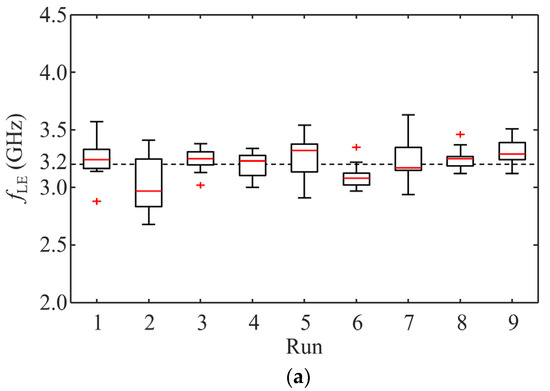
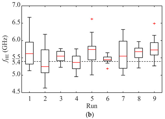
Figure 5.
Distributions of (a) fLE and (b) fHE obtained from the proposed synthesis method for hyperparameter optimization in TM-HPO.
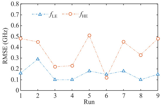
Figure 6.
RMSE comparison between each run in TM-HPO to determine the best hyperparameters adopted in DIM.
To quantitatively determine the best hyperparameters, the RMSE values of Equation (3) were calculated for all runs. The RMSE values of fLE for all runs were 0.16, 0.29, 0.1, 0.1, 0.18, 0.15, 0.18, 0.10, and 0.15 GHz, and those of fHE were 0.48, 0.45, 0.22, 0.23, 0.51, 0.12, 0.45, 0.33, and 0.48 GHz. The error values in (4) for each run were 6.94, 8.70, 3.60, 3.69, 7.53, 3.45, 6.98, 4.65, and 6.79%, as summarized in Table 5. Since the sixth run showed the lowest value, the hyperparameters of the sixth run of the OA were chosen as the best hyperparameters for DIM. The configuration of the sixth run is the constant neuron structure, including NL1 of 64, M of 16, and LR of 0.005.
Table 5.
Summary of RMSE and error values for TM-HPO.
3.2. Synthesis Case 1: HD-EBG Structure with Constant FBW
With the best hyperparameter determined for TM-HPO, the first demonstration of the HD-EBG synthesis method was performed. The design case considered here was the synthesis of HD-EBG structures comprising different stopbands with a constant FBW. For the constant FBW case, the FBW of the HD-EBG structure was assumed to be 0.53, which is typically required in high-speed packages and PCBs. Three TVs with fLT and fHT values of (2.50 GHz, 4.30 GHz), (3.10 GHz, 5.33 GHz), and (3.50 GHz, 6.02 GHz) were considered, which are represented as TVs 1, 2, and 3. HD-EBG structures for TVs 1, 2, and 3 were synthesized using the proposed DIM. The slotted patches and slot dimensions are presented in Figure 7 and Table 6, respectively. One must note that TM-HPO was not repeated because the best hyperparameters had already been acquired. The fL error values (|fLE(N_DIM) − fLT|/fLT × 100) of TVs 1, 2, and 3 were 0.4, 1.0, and 0.9%, while the fH error values (|fHE(N_DIM) − fHT|/fHT × 100) were 0.7, 1.1, and 0.7%, respectively. All errors were less than 5%. The FBW of the synthesized TVs 1, 2, and 3 was 0.539, 0.528, and 0.528, respectively. Therefore, DIM achieved the synthesis of HD-EBG structures for a constant FBW objective.
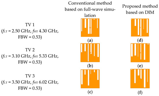
Figure 7.
HD-EBG patches synthesized using the conventional method with a forward model of full-wave simulation and the proposed method with a DNN forward model for different stopbands, maintaining the same FBW. (a–c) are the synthesis results of TV 1, 2, and 3, respectively, using the conventional method based on full-wave simulation and (d–f) are the synthesis results of TV 1, 2, and 3, respectively, using the proposed method based on DIM.
Table 6.
Summary of synthesis results in Figure 7 (units: mm).
Additionally, HD-EBG synthesis using a conventional method was performed for comparison with the DIM results. The conventional method comprises a forward model based on full-wave simulation and GA optimization, as described in [14]. Unlike the proposed method, fL and fH were iteratively estimated using only the FEM solver. The chromosome and population sizes are the same as those used in the proposed method. In the conventional method, GA optimization is repeated 1000 times, and it does not require a verification step. The best solution is chosen as the one with the lowest fL and fH errors among the GA results in the conventional method.
The results of the conventional method are presented in Figure 7 and Table 6. The fL and fH errors of the conventional method were <5.0%. The FBW values of the conventional method for TVs 1, 2, and 3 were 0.550, 0.537, and 0.538, respectively, whereas those of the proposed method were 0.539, 0.528, and 0.528, respectively. The results verified that the proposed DIM synthesizes the HD-EBG structures with different stopbands, while they are constant for FBW. Interestingly, due to the non-uniqueness of the HD-EBG structure, the conventional and proposed methods synthesize different HD-EBG structures, as shown in Figure 7. However, they have the same cutoff frequencies. This was confirmed by comparing the dispersion results, as shown in Figure 8. The dispersion characteristics of TVs 1, 2, and 3 were extracted from the HD-EBG structures obtained using conventional and proposed methods. The stopband characteristics of the proposed method were similar to those of the conventional method, even though they exhibited different slot dimensions, which shows multiple solutions for HD-EBG synthesis.
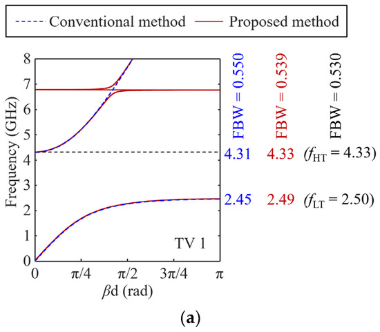
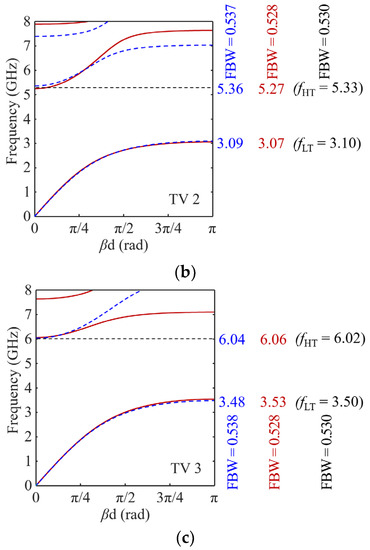
Figure 8.
Dispersion analysis of HD-EBG structures with constant FBW of (a) TVs 1, (b) 2, (c) and 3 synthesized using the conventional and proposed methods.
3.3. Synthesis Case 2: HD-EBG Structure with fH Extension
The other design case for the DIM demonstration is to extend the stopband bandwidth by increasing fH with a constant fL. The design change in this scenario is challenging in the practical design of EBG structures. Consider that the HD-EBG structure with an fLT of 3.2 GHz and fHT of 5.0 GHz (i.e., TV 4) was initially designed, and fH should have been changed to 5.4 (i.e., TV 5) and 5.8 GHz (i.e., TV 6). First, the initial design of the HD-EBG structure (TV 4) was synthesized using the proposed DIM. The synthesized slot dimensions (Ls1, ws1, Ls2, ws2, Ls3, ws3, Ls4, ws4, Ls5, ws5, Ls6, and ws6) are 2.56, 0.50, 0.10, 0.27, 0.10, 0.10, 4.65, 0.44, 4.80, 0.27, 2.33, and 0.15 mm. The fLE and fHE of TV 4 are 3.17 and 4.94 GHz, respectively. The errors are only 0.9 and 1.2%.
To extend a stopband bandwidth from the initial design, DIM synthesizes the HD-EBG structures with fH values of 5.4 (TV 5) and 5.8 GHz (TV 6), respectively. Their slot dimensions are summarized in Table 7. It is shown in the synthesized results that the fLE and fHE of TV 5 are 3.21 and 5.39 GHz, respectively. The errors regarding fLT and fHT are 0.3 and 0.2%, respectively. For TV 6, the fLE and fHE are 3.14 and 5.80 GHz. The errors are 1.9 and 0%. All of the errors in the synthesized results are <5.0%.
Table 7.
Summary of synthesis results in Figure 9 (units: mm).
Examining the synthesis results of the conventional method, the fL and fH errors for TVs 4, 5, and 6 are 2.2, 1.4, 0.6, 0.6, 0.6, and 0.2%, respectively. Compared to the maximum error in the conventional method, it is concluded that the proposed DIM achieves accurate results. In this design challenge, it is interesting that the solutions of the DIM and conventional methods are different, as shown in Figure 9, although their dispersion characteristics are quite similar, as shown in Figure 10. As shown here, it is demonstrated that the proposed DIM solves the design challenge of extending the stopband bandwidth while maintaining fL.
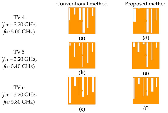
Figure 9.
Synthesized EBG patches of the conventional and proposed methods for TVs 4, 5, and 6 by broadening a stopband bandwidth with a constant fL. (a–c) are the synthesis results of TV 4, 5, and 6, respectively, using the conventional method based on full-wave simulation, and (d–f) are the synthesis results of TV 4, 5, and 6, respectively, using the proposed method based on DIM.
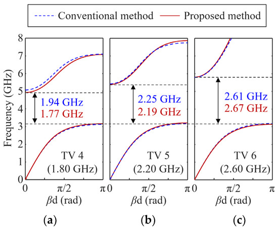
Figure 10.
Dispersion analysis of HD-EBG structures extending a stopband bandwidth with a constant fL of TVs (a) 4, (b) 5, and (c) 6, synthesized via the conventional and proposed methods.
A crucial advantage of the proposed method is the substantial reduction in synthesis time, as shown in Figure 11. In the scenario of constant FBW, the synthesis times of TVs 1, 2, and 3 using the conventional method are 50,946, 55,111, and 45,909 s, respectively, while those of the DIM are 767, 520, and 706 s, respectively. The proposed DIM remarkably achieves a reduction in the synthesis time of 98.5, 99.1, and 98.5%, compared to the conventional method. In the second scenario of fH extension, the conventional method took 25,206 s for TV 4, 43,494 s for TV 5, and 46,750 s for TV 6. However, using the proposed DIM, the synthesis times for TVs 4, 5, and 6 were 400, 80, and 239 s, respectively. The DIM achieves 98.4, 99.8, and 99.5% reductions in computation time for synthesizing TVs 4, 5, and 6, respectively. The proposed DIM shows excellent performance in terms of the computation time for synthesizing the HD-EBG structure. The proposed DIM successfully demonstrates its ability to rapidly synthesize HD-EBG structures and solve the challenging problem of complex design.
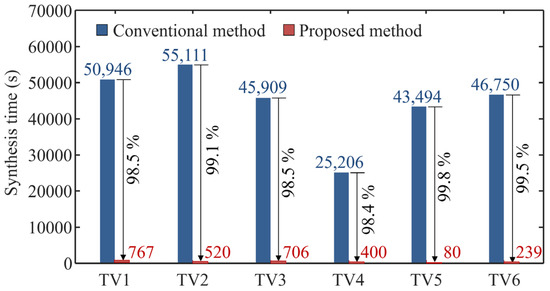
Figure 11.
Comparison of synthesis time between the conventional and proposed methods, which shows the substantial reduction in synthesis time with the proposed method.
4. Conclusions
We presented a DNN-based approach for the rapid synthesis of the HD-EBG structure, which suppresses power/ground noise in high-speed packages and PCBs. The optimal architecture of the neural network for the HD-EBG structure with multiple slots was determined using the OA of the Taguchi method. The neural network structure, learning rate, number of neurons, and hidden layers were considered as factors for hyperparameter optimization. Inverse modeling to solve the synthesis problem was developed by combining a forward model based on DNN and GA optimization. To demonstrate and verify the proposed synthesis method, complicated design problems were considered, namely, the objectives of synthesizing HD-EBG structures with constant FBW and fH extension. The proposed method shows the outstanding characteristics in terms of reducing the synthesis time while solving the problems compared to the conventional method. Using the proposed method, the maximum synthesis time was reduced by 99.8%. The proposed method achieves a fast and accurate synthesis of the HD-EBG structure. The proposed method efficiently overcomes complex design challenges requiring flexible design capabilities. We can extend the proposed method to other EBG structures by considering more datasets including other design variables such as unit cell length, patch size, and position. The proposed method also reduces the threshold of the design of EBG structures and enables engineers in other fields to adopt it for noise problems in high-speed packages and PCBs. Further research can explore the optimization of ANN configurations to reduce the amount of training data while maintaining synthesis result accuracy. Additionally, the proposed method can be experimentally demonstrated for EBG arrays in high-speed packages and PCBs.
Author Contributions
Conceptualization, S.S. and M.K.; methodology, M.K.; software, S.S.; validation, S.S. and M.K.; formal analysis, S.S. and M.K.; writing—original draft preparation, S.S. and M.K.; visualization, S.S. and M.K.; supervision, M.K.; project administration, M.K.; funding acquisition, M.K. All authors have read and agreed to the published version of the manuscript.
Funding
This work was supported by the National Research Foundation of Korea (NRF) grant, funded by the Korean government (Ministry of Science and ICT) (NRF-2019R1C1C1005777).
Data Availability Statement
The data that support the findings of this study are available on request from the corresponding author. The data are not publicly available due to privacy or ethical restrictions.
Conflicts of Interest
The authors declare no conflict of interest.
References
- Wu, T.-L.; Chuang, H.-H.; Wang, T.-K. Overview of Power Integrity Solutions on Package and PCB: Decoupling and EBG Isolation. IEEE Trans. Electromagn. Compat. 2010, 52, 346–356. [Google Scholar] [CrossRef]
- Abhari, R.; Eleftheriades, G. Metallo-dielectric electromagnetic bandgap structures for suppression and isolation of the parallel-plate noise in high-speed circuits. IEEE Trans. Microw. Theory Tech. 2003, 51, 1629–1639. [Google Scholar] [CrossRef]
- Lee, J.; Kim, H.; Kim, J. High dielectric constant thin film EBG power/ground network for broad-band suppression of SSN and radiated emissions. IEEE Microw. Wirel. Compon. Lett. 2005, 15, 505–507. [Google Scholar] [CrossRef]
- Kim, M.; Koo, K.; Hwang, C.; Shim, Y.; Kim, J.; Kim, J. A Compact and Wideband Electromagnetic Bandgap Structure Using a Defected Ground Structure for Power/Ground Noise Suppression in Multilayer Packages and PCBs. IEEE Trans. Electromagn. Compat. 2012, 54, 689–695. [Google Scholar] [CrossRef]
- Kim, M.; Kam, D.G. A Wideband and Compact EBG Structure With a Circular Defected Ground Structure. IEEE Trans. Components, Packag. Manuf. Technol. 2013, 4, 496–503. [Google Scholar] [CrossRef]
- Wei, P.-S.; Tsai, M.-H.; Hsu, S.-K.; Shen, C.-K.; Wu, T.-L. An Electromagnetic Bandgap Structure Integrated With RF LNA Using Integrated Fan-Out Wafer-Level Package for Gigahertz Noise Suppression. IEEE Trans. Microw. Theory Tech. 2018, 66, 5482–5490. [Google Scholar] [CrossRef]
- Lin, D.-B.; Wang, T.-H.; Chiang, J.-W. Suppression of Wideband Simultaneous Switching Noise Through Application of a Partial Electromagnetic Band-Gap Structure in Multilayer Printed Circuit Boards. IEEE Trans. Electromagn. Compat. 2020, 62, 1247–1255. [Google Scholar] [CrossRef]
- Choi, J.; Govind, V.; Swaminathan, M.; Bharath, K. Noise Isolation in Mixed-Signal Systems Using Alternating Impedance Electromagnetic Bandgap (AI-EBG) Structure-Based Power Distribution Network (PDN). IEEE Trans. Adv. Packag. 2009, 33, 2–12. [Google Scholar] [CrossRef]
- Toyota, Y.; Engin, A.E.; Kim, T.H.; Swaminathan, M. Stopband Analysis Using Dispersion Diagram for Two-Dimensional Electromagnetic Bandgap Structures in Printed Circuit Boards. IEEE Microw. Wirel. Components Lett. 2006, 16, 645–647. [Google Scholar] [CrossRef]
- Mohajer-Iravani, B.; Ramahi, O.M. Suppression of EMI and Electromagnetic Noise in Packages Using Embedded Capacitance and Miniaturized Electromagnetic Bandgap Structures With High-k Dielectrics. IEEE Trans. Adv. Packag. 2007, 30, 776–788. [Google Scholar] [CrossRef]
- Wang, T.-K.; Han, T.-W.; Wu, T.-L. A Novel Power/Ground Layer Using Artificial Substrate EBG for Simultaneously Switching Noise Suppression. IEEE Trans. Microw. Theory Tech. 2008, 56, 1164–1171. [Google Scholar] [CrossRef]
- Raimondo, L.; De Paulis, F.; Orlandi, A. A Simple and Efficient Design Procedure for Planar Electromagnetic Bandgap Structures on Printed Circuit Boards. IEEE Trans. Electromagn. Compat. 2010, 53, 482–490. [Google Scholar] [CrossRef]
- Kim, T.H.; Swaminathan, M.; Engin, A.E.; Yang, B.J. Electromagnetic Band Gap Synthesis Using Genetic Algorithms for Mixed Signal Applications. IEEE Trans. Adv. Packag. 2009, 32, 13–25. [Google Scholar] [CrossRef]
- Zhu, H.-R.; Wang, J.-B.; Sun, Y.-F.; Wu, X.-L.; Mao, J.-F. A Novel Automatically Designed EBG Structure by Improved GA for Ultrawideband SSN Mitigation of System in Package. IEEE Trans. Adv. Packag. Manuf. Technol. 2020, 10, 123–133. [Google Scholar] [CrossRef]
- Creech, G.; Paul, B.; Lesniak, C.; Jenkins, T.; Calcatera, M. Artificial neural networks for fast and accurate EM-CAD of microwave circuits. IEEE Trans. Microw. Theory Tech. 1997, 45, 794–802. [Google Scholar] [CrossRef]
- Zhang, Q.-J.; Gupta, K.C.; Devabhaktuni, V.K. Artificial neural networks for RF and microwave design—From theory to practice. IEEE Trans. Microw. Theory Tech. 2003, 51, 1339–1350. [Google Scholar] [CrossRef]
- Rayas-Sanchez, J. EM-Based Optimization of Microwave Circuits Using Artificial Neural Networks: The State-of-the-Art. IEEE Trans. Microw. Theory Tech. 2004, 52, 420–435. [Google Scholar] [CrossRef]
- Mkadem, F.; Boumaiza, S. Physically Inspired Neural Network Model for RF Power Amplifier Behavioral Modeling and Digital Predistortion. IEEE Trans. Microw. Theory Tech. 2011, 59, 913–923. [Google Scholar] [CrossRef]
- Jin, J.; Feng, F.; Zhang, J.; Yan, S.; Na, W.; Zhang, Q. A Novel Deep Neural Network Topology for Parametric Modeling of Passive Microwave Components. IEEE Access 2020, 8, 82273–82285. [Google Scholar] [CrossRef]
- Xiao, Y.; Leung, K.W.; Lu, K.; Leung, C.-S. Mode Recognition of Rectangular Dielectric Resonator Antenna Using Artificial Neural Network. IEEE Trans. Antennas Propag. 2022, 70, 5209–5216. [Google Scholar] [CrossRef]
- Beyene, W.T. Application of Artificial Neural Networks to Statistical Analysis and Nonlinear Modeling of High-Speed Interconnect Systems. IEEE Trans. Comput. Des. Integr. Circuits Syst. 2006, 26, 166–176. [Google Scholar] [CrossRef]
- Kim, H.; Sui, C.; Cai, K.; Sen, B.; Fan, J. Fast and Precise High-Speed Channel Modeling and Optimization Technique Based on Machine Learning. IEEE Trans. Electromagn. Compat. 2017, 60, 2049–2052. [Google Scholar] [CrossRef]
- Zhang, H.H.; Xue, Z.S.; Liu, X.Y.; Li, P.; Jiang, L.; Shi, G.M. Optimization of High-Speed Channel for Signal Integrity With Deep Genetic Algorithm. IEEE Trans. Electromagn. Compat. 2022, 64, 1270–1274. [Google Scholar] [CrossRef]
- Sim, S.; Kim, M. Convolutional Neural Network-based Design of EBG Structures in High-Speed Packages and PCBs. In Proceedings of the 2021 IEEE International Joint EMC/SI/PI and EMC Europe Symposium, Raleigh, NC, USA, 26 July–13 August 2021; p. 422. [Google Scholar] [CrossRef]
- Jin, J.; Zhang, C.; Feng, F.; Na, W.; Ma, J.; Zhang, Q.-J. Deep Neural Network Technique for High-Dimensional Microwave Modeling and Applications to Parameter Extraction of Microwave Filters. IEEE Trans. Microw. Theory Tech. 2019, 67, 4140–4155. [Google Scholar] [CrossRef]
- Jin, J.; Feng, F.; Zhang, W.; Zhang, J.; Zhao, Z.; Zhang, Q.-J. Recent Advances in Deep Neural Network Technique for High-Dimensional Microwave Modeling. In Proceedings of the 2020 IEEE MTT-S International Conference on Numerical Electromagnetic and Multiphysics Modeling and Optimization (NEMO), Hangzhou, China, 7–9 December 2020; pp. 1–3. [Google Scholar]
- Wu, Y.; Pan, G.; Lu, D.; Yu, M. Artificial Neural Network for Dimensionality Reduction and Its Application to Microwave Filters Inverse Modeling. IEEE Trans. Microw. Theory Tech. 2022, 70, 4683–4693. [Google Scholar] [CrossRef]
- Clevert, D.-A.; Unterthiner, T.; Hochreiter, S. Fast and accurate deep network learning by exponential linear units (elus). arXiv 2015, arXiv:1511.07289. [Google Scholar]
Disclaimer/Publisher’s Note: The statements, opinions and data contained in all publications are solely those of the individual author(s) and contributor(s) and not of MDPI and/or the editor(s). MDPI and/or the editor(s) disclaim responsibility for any injury to people or property resulting from any ideas, methods, instructions or products referred to in the content. |
© 2023 by the authors. Licensee MDPI, Basel, Switzerland. This article is an open access article distributed under the terms and conditions of the Creative Commons Attribution (CC BY) license (https://creativecommons.org/licenses/by/4.0/).