1. Introduction
High bandwidth memory 2 (HBM2) is built by stacking up to eight dynamic random-access memory (DRAM) dies over a base logic die. Each stacked die is connected to others via through-silicon vias (TSVs), which deliver power and signals. HBM2 is typically composed of four or eight stacks of core dynamic random-access memory (DRAM) dies.
The vertically stacked structure of HBM2 provides a small form factor, but its power density is three times higher than that of the graphics double data rate 5 (GDDR5) [
1]. The relatively small size of HBM2 creates more challenges in handling the heat issues inside HBM2. The HBM2 stacks are 720 µm high in one implementation, including the base logic die [
2]. Each core DRAM die is 50 µm thick, and a 19 µm underfill is added between the dies [
3].
In this vertically stacked structure, the heat generated from the base logic die spreads to the core DRAM dies and package surfaces. Consequently, each stacked die can experience different temperatures, and a thermal gradient can occur in the paths from the base die to the package surface [
4,
5].
Because HBM2 is composed of multiple DRAM dies, it inherits the thermal characteristics of DRAM and the diagnostic limitations owing to the stacked structure [
6,
7]. The retention issue in DRAM is caused by the leakage current from the storage capacitors inside the memory bit cells, which is generally the most sensitive to temperature [
8,
9,
10,
11,
12].
Many previous studies have proposed different methods for reducing retention errors. Three main categories used to mitigate DRAM retention errors are the bit repair methods [
13,
14,
15,
16], error correction code-based (ECC-based) mitigation techniques [
17,
18], and temperature-aware refresh (TAR) [
19,
20]. TAR is a method of changing the refresh interval chosen for each stack die or DRAM bank depending on the temperature during DRAM operations. The TAR provides system adaptability to temperature variations, which is the key technique for handling retention errors.
If the heat does not properly dissipate through the stacked structure in the HBM, retaining the bit cells may be problematic. The manufacturer generally embeds temperature sensors inside an HBM to implement TAR-based techniques. The HBM controller can access the sensors using the IEEE1500 protocol and uses temperature information to adjust the DRAM refresh intervals [
2]. It is a good method if the HBM is accessed directly with DA test ports in the wafer-level testing. However, this method is not useful for users with already integrated HBM. The DA test port is not accessible after assembly, and the test system in this study also does not provide access to the DA test port.
In this study, the temperature sensitivity of DRAM was used as the key idea to analyze the temperature variations in stacked dies experimentally. If the temperature sensitivity can be determined for the core DRAM die inside the HBM2, then the temperature differences of the dies can be estimated indirectly.
Dynamic retention errors were used in this study to determine the temperature sensitivity of DRAM cells. In the previous studies, retention errors were studied in a single DRAM cell [
8,
21] or a single DRAM device [
22,
23,
24,
25,
26]. Because the retention errors in this study were measured using HBM2, the error information should contain the temperature information imposed by the HBM2 structure. The errors were reversely used to study temperature variations in the stack dies.
The rest of this paper is organized as follows:
Section 2 explains the hardware platform organization used for dynamic retention testing.
Section 3 discusses the dynamic retention test environment using custom design blocks.
Section 4 discusses temperature control, sensing the environment, and the relationship between the sensed temperatures. In
Section 5, the relationship between the error count, refresh time, and temperature is discussed based on the results and statistics for a single channel.
Section 6 discusses the temperature difference across the channels using the Z-values over various refresh times at a fixed temperature.
Section 7 estimates the temperature difference across all the channels by comparing the Z-difference between all the channels and two temperatures. Finally,
Section 8 concludes this paper.
2. FPGA Chip Organization
The experiments in this study were performed using an Intel Stratix 10 MX development kit, which comprises an FPGA chip, power supply, and peripherals. The FPGA chip internally integrates two HBM2 devices, and its organization is shown in
Figure 1, where only one HBM2 device is shown. The two HBM2s are referred to as the top HBM2, and bottom HBM, based on their positions relative to an FPGA die.
The FPGA die implements two major design blocks: the test logic and the interface block. The test logic controls the dynamic retention tests, the design structure of which will be discussed in the next section. The interface block contains the HBM2 memory controller, PHY, and I/O ports to connect to the HBM2 stack. The bridge is an interface that connects the FPGA fabric and devices inside the FPGA chip [
27]. The HBM2 device was connected to its controller through an interface block inside the FPGA fabric and a bridge interface outside the FPGA fabric.
Each HBM2 has eight channels, and two channels are assigned to each stack die. Each HBM2 channel can be further organized using two pseudo-channels. Each channel is accessed independently of the other channels. The two pseudo-channels operate semi-independently; they share the row and column command bus as well as the clock (CK) and clock enable (CKE).
A single channel has an independent advanced extensible interface (AXI) assigned to two pseudo-channels and has one advanced peripheral bus (APB) interface shared by both pseudo-channels [
27]. The AXI interface follows the AXI bus protocol, which uses the handshake method. The AXI interface supports 256 bits of write-data width and 256 bits of read-data width. All the HBM2 spaces are accessible by the AXI interface. All measurements in this paper cover the full area of the channels.
The APB interface is used to access the configuration and status register of HBM2 and control the refresh interval. The refresh interval of all the channels is independently controlled, and in this paper, a separate refresh interval controller is adopted for each channel. The retention test was performed at the pseudo-channel level, and the pseudo-channels were sequenced.
3. Dynamic Retention Test Environment
3.1. Test Logic Design Blocks
Figure 2 is the redrawing of
Figure 1, with four major sub-blocks in the test logic blocks: the NIOS II processor, peripheral interconnect, programmable memory built-in self-test (PMBIST), and PMBIST–HBM interface. The HBM2 memory operation speed was 800 MHz, and the FPGA internal clock was 200 MHz.
The NIOS II processor is an internal processor that controls the test logic. The peripheral interconnect block connects the NIOS II processor and the other design blocks, as indicated by the arrows in
Figure 2. It transmits the control signals for the test operations from the NIOS II processor to the PMBIST. Additionally, the interconnects block includes the bus for controlling the refresh interval of the HBM2 controller and the bus receiving the base die temperature from an HBM2 [
28].
PMBIST is responsible for issuing memory operation commands, addresses, and data to HBM2 in coordination with NIOS II. The PMBIST–HBM interface is a module that connects the PMBIST and HBM2 controllers.
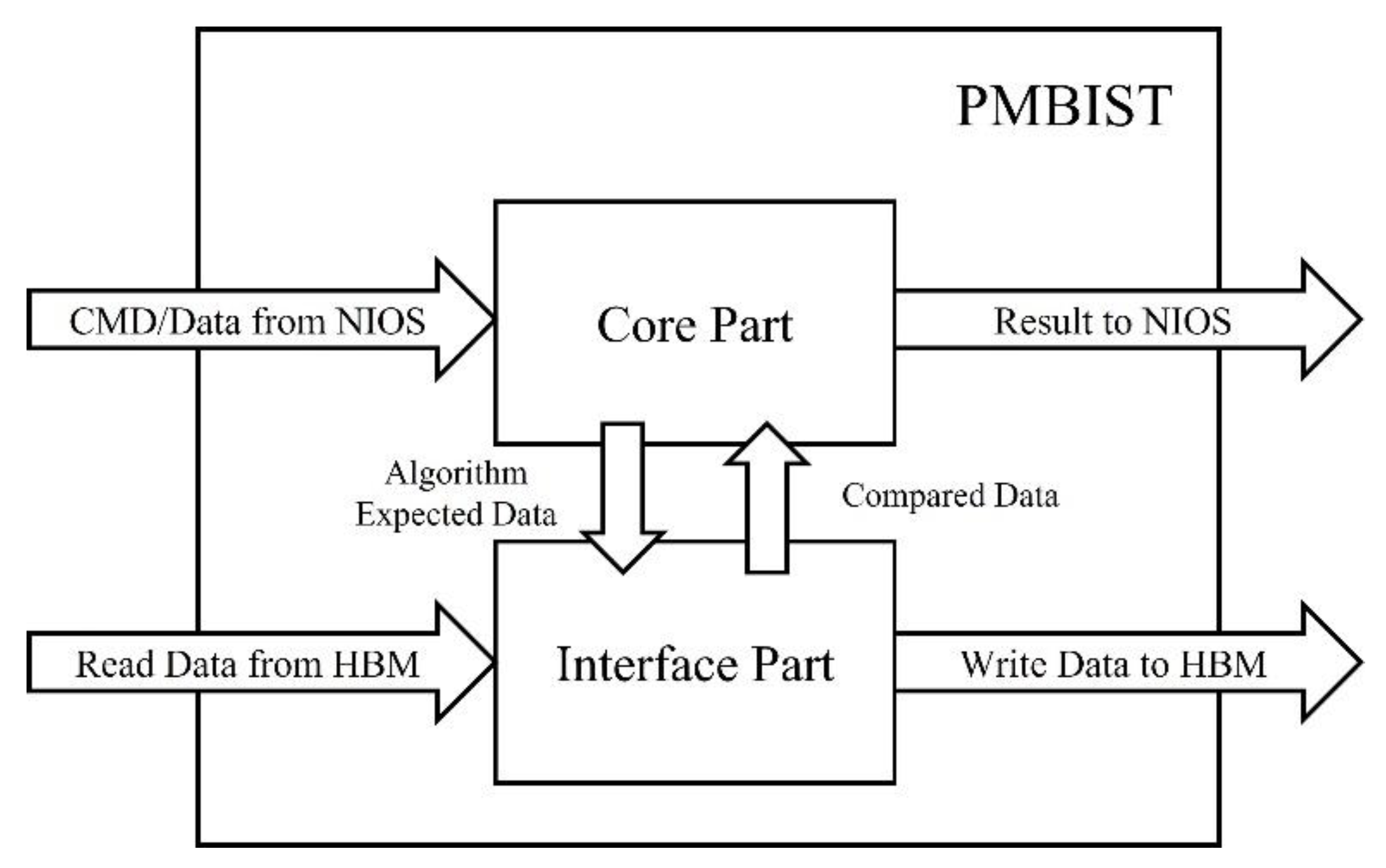
3.2. PMBIST Design Blocks
The PMBIST block issues write/read commands and address the sequences programmed by the user. PMBIST is primarily divided into hardware and software parts. The hardware part is further divided into core and interface parts, as shown in
Figure 3. The core part controls the entire BIST algorithm and generates the addresses and commands. In addition, it receives commands from the NIOS II processor and returns the results from the issued memory commands.
The interface part generates the data bit patterns and compares the read data from HBM2 with the expected data. In addition, it includes several sub-modules to connect the PMBIST and memory controller.
The software part of PMBIST is the firmware of the NIOS II processor and performs three primary functions. The first function is to transmit the test algorithm and data pattern specified by a user to the hardware part and specify the test target address range and other settings, such as PMBIST configurations. The second function adjusts the refresh interval by accessing the APB interface of the HBM2 controller directly.
Finally, the third function retrieves the temperature value from the FPGA module that accesses the base die temperature in HBM2.
3.3. Dynamic Retention Test
Our test design is connected to either an APB or AXI interface based on the accessed and controlled information type. The APB interface controls the refresh interval. The refresh interval is orthogonally controlled regardless of the operation of an HBM2 [
27], which makes it possible to implement a dynamic retention test.
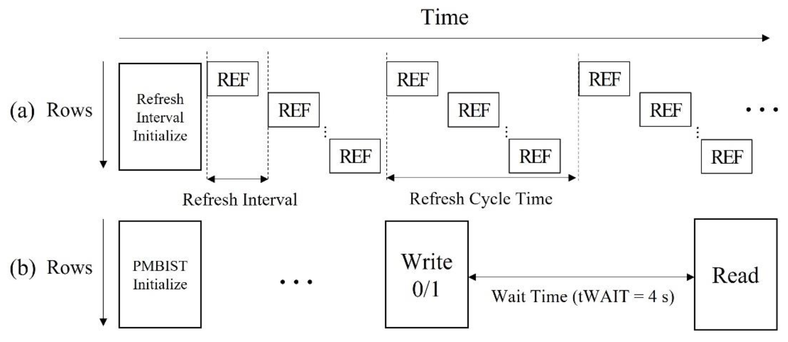
A typical retention test measures the time elapsed from stopping a refresh until a cell’s value flips. A retention test was performed in this study by varying the refresh intervals. The refresh operations were performed continuously during the retention test.
Figure 4 shows the test sequences used in this study.
Figure 4a demonstrates that refreshes are sequentially performed for all the rows in a bank. The refresh interval is the time interval between two consecutive refreshes. The refresh cycle time (RCT) is the time required to refresh all the rows in a bank. The maximum refresh interval configurable in the test logic was 249 µs, which could provide sufficient error distributions for this study. The maximum RCT was 2.048 s (249 µs × 8192). A bank in HBM2 requires 8192 refreshes based on the JEDEC HBM2 specification [
2]. The NIOS II processor in the FPGA initializes the refresh interval by using the refresh counter value in the test logic.
Figure 4b shows the retention test performed using the PMBIST when configured with algorithmically ordered write/read commands and address sequences based on the user’s choices. The retention test starts with the PMBIST initialization of the HBM2 memory. Once the target memory space is initialized, PMBIST waits for a predetermined wait time without any memory operations before checking all the cells concerning the initialized values. The wait time can be any value greater than that of the RCT. We used 4 s (tWAIT) in most experiments. The wait time in a unit measurement time is fixed at 4 s, which should be sufficiently large enough to cover marginal retention errors. In the experiments, the refresh cycle can be configured between 64 ms and 2048 ms; the entire test area is refreshed at least two times within the 4 s wait time. It was observed that increasing the wait time above 4 s did not change the results. The precision of the temperature estimation was not expected to increase. On the other hand, if the wait time is reduced to 2 s or less, sufficient retention errors may not occur depending on the refresh cycle time, and the temperature resolution can be negatively affected.
A similar argument can be applicable to the number of repetitions. In this experiment, the number of repetitions was 20 times, which is sufficiently large, and more repetitions would not affect the temperature analysis. The number of repetitions was set to cover sufficient temperature variations. The temperature variation during the measurement time is described in detail with figures in
Section 4.
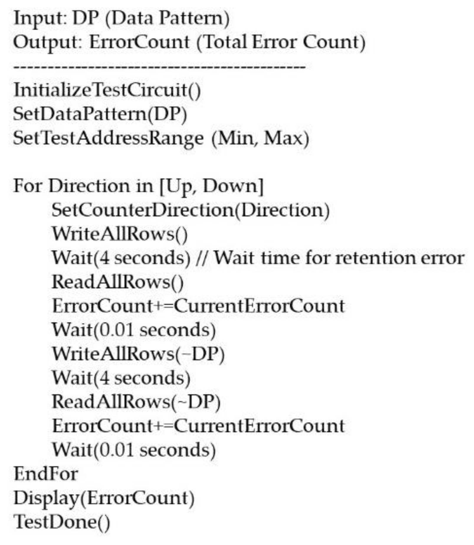
Figure 5 shows the pseudo-code for a retention test. InitializeTestCircuit() includes the refresh interval initialize and PMBIST initialize. SetCounterDirection(Direction) sets the address direction, and SetDataPattern(DP) and parameter DP are set to the data pattern. The test combined the address direction, ‘up’ or ‘down,’ and the ‘0’ or ‘1’ data pattern. The four combinations, ‘up-0’, ‘up-1’, ‘down-0’, and ‘down-1’, are executed in the order shown in
Figure 5. The error count results in this paper added up the numbers of four sequences because it was hard to know the ratio of true-cell and anti-cell.
A 4 s wait time was sufficient for the maximum RCT. Depending on the refresh interval, the same cell can be refreshed multiple times during the wait time. To differentiate a typical retention test without refreshes, as mentioned earlier, the retention test in this study is referred to as the dynamic retention test. This is because the initialization and read validation steps use the same refresh intervals during the wait time, and the retention test can be affected by the two steps.
4. Temperature Controlling and Sensing Environment in FPGA Development Kit
During retention testing, the temperatures at various locations are monitored.
Figure 6 shows the development kit with external temperature sensors around the FPGA chip.
In this study, five sensors were added to the kit to measure the temperature. Two of the three temperature sensors are located outside the FPGA chip, and the third sensor (not shown) is located inside the HBM2 [
28].
The ambient temperature (T
A) is the temperature inside the temperature chamber (
Figure 7) and is located at the grille of the development kit. The heat sink temperature (T
S) is the temperature at the top of the FPGA chip heat sink. The three temperatures were monitored constantly to ensure reasonable temperature conditions.
Unlike the two external temperatures, the logic-die temperature (T
L) is the temperature in the HBM2 and can be accessed through an Intel temperature sensor module [
28], as shown in
Figure 2. T
L is the key temperature that affects the retention time of the embedded DRAM memory. Currently, the temperature is limited to 80 °C, and the kit stops working with warning signs. Therefore, all the experiments were performed with such limitations.
Figure 7 displays the temperature control environment that uses a temperature chamber and a fan control subsystem using a microcontroller as well as a computer. The temperature chamber maintained the ambient temperature close to the desired temperature. The temperature chamber is the forced convection oven. It has a 150 L internal capacity, a 1/4 horsepower convection motor, and a 200 °C temperature limitation. The test board is installed on a non-conductive rubber pad with a center shelf at the center of the chamber. We continuously performed the test for 24 h under an ambient temperature of 50 °C. The chamber was maintained T
A at 50 °C for all the experiments unless mentioned otherwise.
The microcontroller is an Arduino Uno, which controls the two 40 mm fans near the FPGA chip and monitors the two external temperatures, T
A, and T
S, as shown in
Figure 7. The temperature T
S is controlled by the speed of the two cooling fans, and the speed is controlled through pulse width modulation (PWM) by the microcontroller. The PWM magnitude of the cooling fans is influenced by the temperature difference between the T
S and the desired temperature. Furthermore, the larger the T
S difference, the higher the PWM value is. When the temperature difference decreases due to the cooling fan, the PWM value gradually decreases until cooling is no longer required. To stabilize the temperature during the measurement, the microcontroller monitors the temperature every second and tracks the T
S value to reliably achieve the target T
L. Measurements were initiated only after the T
S was stabilized with ±1 °C variation for at least 1 min.
Figure 8 shows the heatsink temperature during the measurement time. A single measurement time was 59 s, and 20-times repetitions of the measurement time were 1280 s. The highest temperature during the measurement time was 68.8 °C, and the lowest temperature during the measurement time was 67.7 °C. The heatsink temperature was stable during the measurement time.
Figure 9 shows the three temperatures, T
A, T
S, and T
L, with three different T
S target temperatures. In all three cases, T
A was maintained at 50 °C. T
S gradually increased owing to self-heating by the operating power of the kit. When the heat sink temperature exceeded the target temperature, the fans were immediately activated to reduce it. For all three cases, it was observed that the temperature differences between the heatsink and the desired temperatures were 1–2 °C.
It was observed that the logic-die temperature was always higher than the heatsink temperature. The temperature difference between TS and TL increased with the increase in the target temperature. For example, a 3.4 °C temperature gap was observed when TL was 80 °C.
Figure 10 shows a cross-sectional view of the main thermal flow in the development kit. The dissipated power in the FPGA was assumed to pass through the heatsink to the ambient environment. Suppose that the ambient temperature and dissipated power were maintained constant, and T
L continued to increase. In this case, the temperature gap between T
S and T
L would be expected to increase, as shown in
Figure 9. The thermal conductivity from the logic dies in HBM2, through the stacked DRAM dies, to the package seems to decrease as T
L increases.
5. Single Channel Experimental Results and Statistics
Figure 11 shows the retention test results in the Pseudo-channel 0 of Channel 0 with T
L maintained at 70 °C. The
x-axis is the RCT (refresh interval × 8 k), which gradually increases to see the relation to the error counts. The
y-axis represents the number of retention error bits.
The RCT started from 0.064 s, which is twice the minimum retention time in HBM2, according to JEDEC [
2]. No errors were observed until the RCT increased to 0.5 s, as shown by the fifth dot from the left in
Figure 11; the error count was four. The RCT then increased to 2.048 s, which provided a sufficient error count when studying the retention time. The error count increased to 37,837 with a 2.048 s RCT.
As the RCT gradually increased, the error count increased exponentially, which is a common characteristic of component DRAMs. The same trend was observed in all the channels and is further discussed in the next section.
We assumed that the retention error counts followed a normal distribution, which was observed in previous observations in DRAMs [
8].
Figure 12 displays the lognormal distribution plot in terms of the Z-values of the same data in
Figure 11. The
x-axis represents the RCT, expressed on a log scale, and the
y-axis represents the Z-value.
The Z-value is the logarithmic standard deviation multiplied by the distribution mean. All the data appear below –4.4, which indicates that the error bits in
Figure 12 belong to a tail distribution of less than 0.003% of all the memory cells.
Two slopes were observed at the boundary of 0.767 on the
x-axis. The left side of the boundary is referred to as Region 1, and the right side is referred to as Region 2. It was observed that the sloped boundary changed with other parameters, such as the temperature and different channels. Because the slope is typically related to a dominant failure mechanism, it can be assumed that there were failure mechanism changes at the slope boundaries. As the failure mechanism is beyond the scope of this study, we simplified the trend analysis using the trend line, as shown in
Figure 12. In the case of Channel 0, the blue trend line for all the regions shows a slope of 1.07, and the y-intercept is –19.96. The green curve for Region 1 shows a slope of 2.04, and the y-intercept is –32.88. The orange plot for Region 2 shows a slope of 0.85, and the y-intercept is −16.82. Region 1 was not used to compare the slopes because the number of retention errors was insufficient for this study. The slope has been compared to other channel slopes later.
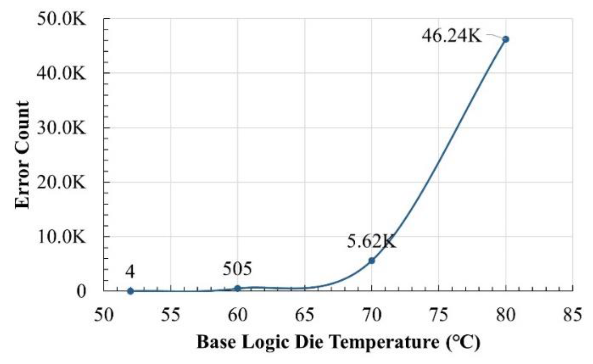
Figure 13 shows the error counts with varying T
L in the same pseudo channel in
Figure 11 when the RCT was 1.28 s. The tests were performed with T
L at 52 °C, 60 °C, 70 °C, and 80 °C. The retention error count exponentially increased with an increase in T
L, which is a typical characteristic of DRAM components. This trend was observed to be similar for all the channels.
Figure 14 shows the retention errors with a varying RCT at T
L of 60 °C, 70 °C, and 80 °C. Additionally, the experiment showed a similar trend for various RCTs, as shown in
Figure 11; however, this is at different scales. Because exponential growth was observed with RCTs above 1.28 s, RCTs were used in most experiments with varying temperatures.
The lognormal Z-value plot in
Figure 15 illustrates the results of the error count separately. As T
L increases, the trend line moves to the left, indicating that a smaller RCT (smaller refresh interval) is required to obtain the same error count. For example, the RCT was 1.022 s at 70 °C and 0.64 s at 80 °C when the Z-value was –5. Additionally, it was observed that the trend line increased with an increase in temperature. For example, when the refresh cycle was 1.406 s, the Z value increased from –4.76 to –4.32 when the T
L increased from 70 °C to 80 °C. The difference in the Z-values over the two temperatures in a refresh cycle is 0.44, which is referred to as the Z-gap.
In
Figure 15, the Z-gap was the largest at an RCT of 0.895 s when the two temperatures were 70 °C and 80 °C in Region 2. It gradually reduced with an increase in RCT; the error bits kept increasing with an increase in RCT, reducing the temperature sensitivity. To determine the temperature sensitivities in stacked DRAM dies, it is recommended to choose a value of RCT that brings the Z-gap near its maximum, called the temperature-sensitive RCT. For analysis, the temperature-sensitive RCT was selected from Region 2, with a larger number of retention error bits. We selected 1.406 s as the temperature-sensitive RCT for discussion.
6. Multiple Channel Experimental Results and Statistics
Figure 16 shows the error counts with a varying RCT with T
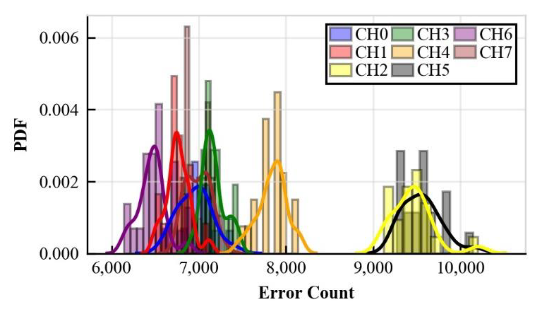
L fixed at 70 °C in all the channels. The channels exhibit a trend similar to Channel 0, discussed in the previous section. The error counts of Channels 2 and 5 were distinctively larger than the other channels. We assume that the process variation is similar for all channels. We can then explain why the retention error of channels 2 and 5 occurs more than the other channels. The two channels are closer to the logic die (the main heat source) compared to the other channels.
In the multi-channel discussions in this section, an important objective is to explore the experimental evidence that certain channels were placed at relatively higher temperatures than other channels owing to the stacked-die structure in HBM2. The error counts owing to the temperature difference were larger than the typical process variation.
Figure 17 displays the Z-value plots for all the channels using the same data as
Figure 16. The section near the RCT at 1.406 s is enlarged to show the changes in the Z-value. The Z-gaps across the channels at the same temperature appear smaller than the Z-gaps among the different temperatures in
Figure 15, which indicates that the temperature difference causes more change in the error counts than the process variation in the eight channels. For example, the Z-gap between the two temperatures, 70 °C, and 80 °C, was 0.44, whereas the maximum Z-gap across the channels was 0.091, which is approximately 4.82 times the difference.
Additionally, in
Figure 17, it can be observed that there are four groups of channels, considering the relative Z-gap magnitudes of all the eight channels: Group 1 includes Channels 2 and 5; Group 2 includes only Channel 4; Group 3 includes Channels 0, 1, 3, and 7; and Group 4 includes only Channel 6.
To demonstrate that the Z-gaps in
Figure 17 are not attributed to the measurement errors, we collected the error counts by repeating the dynamic retention test with T
L at 70 °C and RCT at 1.406 s.
Figure 17 shows the results of the repeated dynamic retention tests for all the channels. Four distinct peaks can be observed in
Figure 18. From left to right, the first peak is formed by Channel 6 only; the second peak is formed by Channels 0, 1, 3, and 7; the third peak is formed by Channel 4, and the fourth peak is formed by Channels 2 and 5. The channels in the peak are the same as those in the four groups, as shown in
Figure 17.
The variation in the error counts in
Figure 18 is translated to the Z-domain in
Figure 16 to show the error ranges that measurements can potentially provide. Because the Z-gap in
Figure 17 is significantly larger than the error bars for each channel, the Z-gap exists primarily owing to the temperature differences.
7. Temperature and Error-Count Relation of HBM2 Channels with Finely Controlling Base Die Temperature
Figure 19 presents the retention error counts in all channels of HBM2 while varying the base logic die temperature from 66 °C to 76 °C in steps of 2 °C. The RCT was fixed at 2.04 s in this experiment. Again, two groups of channels were observed at all temperatures, as shown in
Figure 16.
The dots in
Figure 20 show the Z-values in all the channels with a T
L of 70 °C and a varying RCT. All the dashed lines are based on the error count data from Pseudo-channel 0 in Channel 0. The blue dashed line represents the T
L of 60 °C. The green dashed line represents the T
L of 80 °C.
The red dashed lines show the boundaries of all the channels concerning Channel-0 error counts at a T
L of 70 °C. The lower red dashed line represents the trend of error counts at 70 °C. The upper red dashed line specifies the upper boundary to enclose all the channels’ Z-values; the boundary is located at the two-tenth point between 70 °C and 80 °C. Note that all the Z-value dots in the channels are located between the two dashed red lines. The error count results in all the channels were acquired when the Channel-0 temperature was between 70 °C and 72 °C. In
Figure 9 in
Section 4, when T
S was 68 °C, T
L was 70 °C, which is a 2 °C difference. The 2 °C difference between T
S and T
L in
Figure 9 partly explains the 2 °C boundaries in
Figure 20.
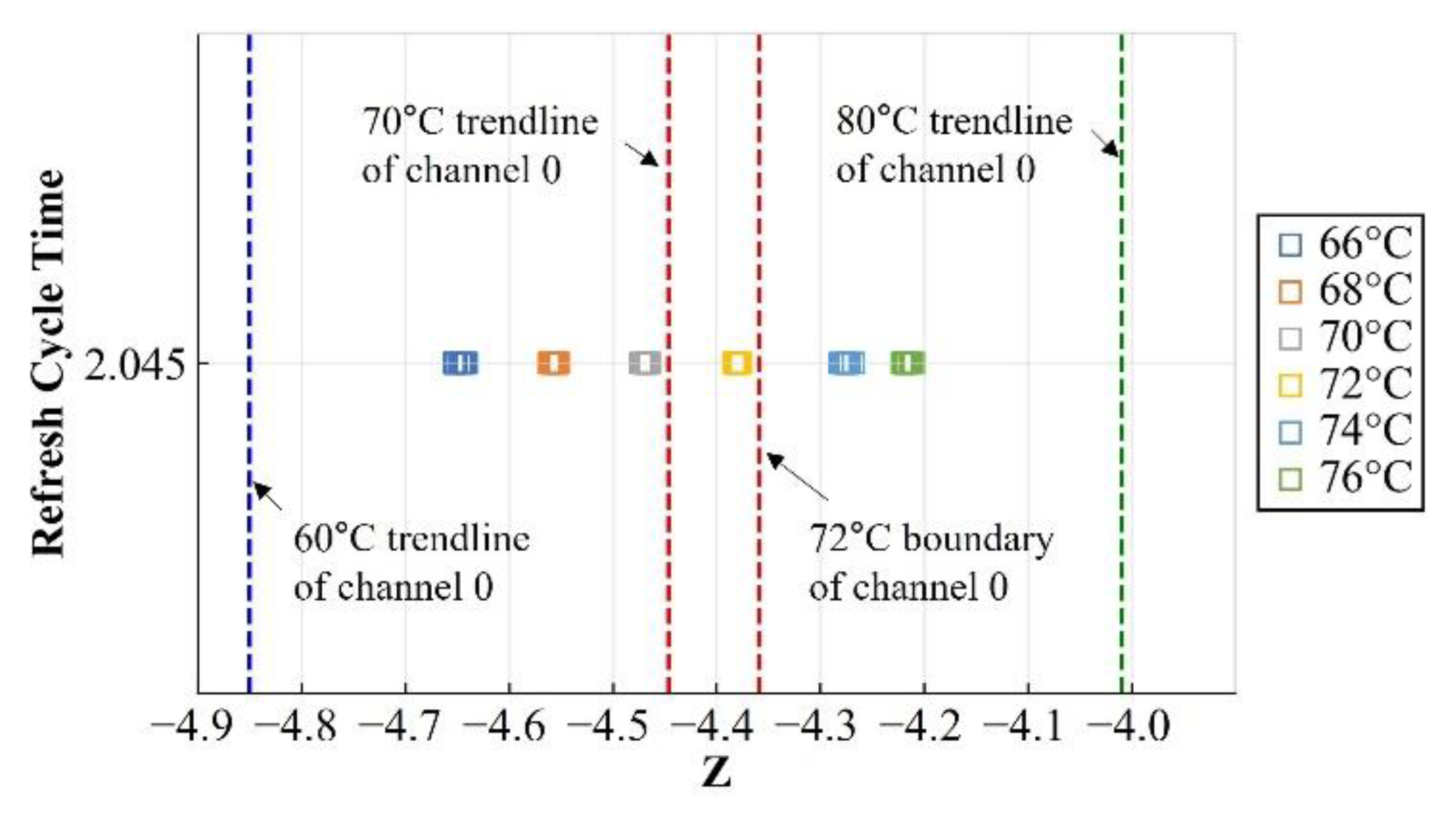
Additionally, dynamic retention tests were performed for Channel 0 with finer temperature control. The dots in
Figure 21 demonstrated the Z-values when T
L varied from 66 °C to 76 °C in 2 °C increments.
The Z-values in the dashed vertical lines are from
Figure 20 when RCT is 2.045 s. The Z-values are expressed as lines instead of dots to emphasize the boundaries. The Z-gap between 70 °C and 72 °C in
Figure 21 is approximately the same as the maximum Z-gap across all the channels at 70 °C. This observation shows that the temperature difference across all the channels can be estimated by observing one-channel error count data with a finer control of T
L.
8. Conclusions
Using the retention error count, we studied the temperature estimation of stacked dies in HBM2. The error count in a single channel is sensitive to temperature and RCT.
The retention error count is exponentially related to the RCT in all the channels, and a lognormal distribution is used to describe the number of cells with different RCT values.
The difference in the Z-values between the different temperatures is referred to as the Z-gap. The Z-value plots for all the channels with a varying RCT and a fixed TL of 70 °C showed Z-gaps across the channels. The maximum Z-gap across the channels was 0.91, which was 4.82 times smaller than the Z-gap between TL of 70 °C and 80 °C in the temperature-sensitive RCT. If eight channels have the same characteristics, it is evident that the error counts affected by the temperature variation are greater than the process variation in the eight channels.
The Z-plot trendlines in Channel 0 at TL of 70 °C and 80 °C calculated the Z-value boundaries for all the channels, which displayed the maximum temperature difference across all the channels as 2 °C at a fixed TL of 70 °C.
The Z-gap with a finely controlled TL in 2 °C increments was approximately the same as the Z-value boundaries across all the channels at a fixed TL of 70 °C. The error counts of a single channel with a finely controlled temperature can be used to estimate the temperature distribution across all the channels.
The temperature estimation method in this paper can be applied to other platforms with a processor, HBM2, and programmable memory operation using BIST. Our BIST engine can perform a programmable refresh interval, which means that the test channel can be selected in a round-robin manner. If it is used in a real system, BIST tests do not have to be performed continuously or can be performed during a maintenance period.
The only impediment that we can think about in applying the proposed method to other HBM2 platforms will be the BIST engine developed in this paper. Since our BIST was implemented in FPGA, which are typically CPU or GPU chips in other platforms, if the BIST feature is replaced by CPU or GPU, the speed of memory access will be slower than the BIST-based access. In our system, BIST also controls the issuing of refresh commands. There is also a possibility that the relatively smaller refresh interval may not be implementable due to the access speed. If the temperature distribution inside the HBM is estimated through the statistical analysis of the retention error using the measurement method, including the BIST proposed in this paper, it will be possible to identify the thermal problem of the HBM and secure its reliability.
Author Contributions
Conceptualization, J.K. and S.B.; methodology, J.K. and S.B.; software, J.K.; validation, J.K.; formal analysis, J.K.; investigation, J.K.; resources, J.K.; data curation, J.K.; writing—original draft preparation, J.K.; writing—review and editing, J.K., S.-J.W., R.F. and S.B.; visualization, J.K.; supervision, S.-J.W., R.F. and S.B.; project administration, S.B.; funding acquisition, S.B. All authors have read and agreed to the published version of the manuscript.
Funding
This work was supported by Cisco Systems Inc. U.S.A. and the Basic Science Research Program through the National Research Foundation of Korea (NRF) funded by the Ministry of Science, ICT & Future Planning (NRF-2020R1H1A2103043).
Data Availability Statement
Not applicable.
Acknowledgments
The EDA tool was supported by the IC Design Education Center (IDEC), Korea.
Conflicts of Interest
The authors declare no conflict of interest.
References
- Sohn, K.; Yun, W.-J.; Oh, R.; Oh, C.-S.; Seo, S.-Y.; Park, M.-S.; Shin, D.-H.; Jung, W.-C.; Shin, S.-H.; Ryu, J.-M.; et al. A 1.2 V 20 Nm 307 GB/s HBM DRAM With At-Speed Wafer-Level IO Test Scheme and Adaptive Refresh Considering Temperature Distribution. IEEE J. Solid-State Circuits 2017, 52, 250–260. [Google Scholar] [CrossRef]
- JEDEC Solid State Technology Association, High Bandwidth Memory (HBM) DRAM, JESD235C. Available online: https://www.jedec.org/standards-documents/docs/jesd235a (accessed on 3 January 2021).
- Agrawal, A.; Huang, S.; Gao, G.; Wang, L.; DeLaCruz, J.; Mirkarimi, L. Thermal and Electrical Performance of Direct Bond Interconnect Technology for 2.5D and 3D Integrated Circuits. In Proceedings of the 2017 IEEE 67th Electronic Components and Technology Conference (ECTC), Orlando, FL, USA, 30 May–2 June 2017; pp. 989–998. [Google Scholar]
- Ramalingam, S. HBM Package Integration: Technology Trends, Challenges and Applications. In Proceedings of the 2016 IEEE Hot Chips 28 Symposium (HCS), Cupertino, CA, USA, 17–19 August 2016; pp. 1–17. [Google Scholar]
- Son, H.-Y.; Oh, T.; Hong, J.-W.; Lee, B.-D.; Shin, J.-H.; Kim, S.-H.; Kim, N.-S. Mechanical and Thermal Characterization of TSV Multi-Chip Stacked Packages for Reliable 3D IC Applications. In Proceedings of the 2016 IEEE 66th Electronic Components and Technology Conference (ECTC), Las Vegas, NV, USA, 31 May–3 June 2016; pp. 356–360. [Google Scholar]
- Farmahini-Farahani, A.; Gurumurthi, S.; Loh, G.; Ignatowski, M. Challenges of High-Capacity DRAM Stacks and Potential Directions. In Proceedings of the Proceedings of the Workshop on Memory Centric High Performance Computing, Dallas, TX, USA, 11 November 2018; ACM: Dallas, TX, USA, 2018; pp. 4–13. [Google Scholar]
- Jun, H.; Cho, J.; Lee, K.; Son, H.-Y.; Kim, K.; Jin, H.; Kim, K. HBM (High Bandwidth Memory) DRAM Technology and Architecture. In Proceedings of the 2017 IEEE International Memory Workshop (IMW), Monterey, CA, USA, 14–17 May 2017; pp. 1–4. [Google Scholar]
- Hamamoto, T.; Sugiura, S.; Sawada, S. On the Retention Time Distribution of Dynamic Random Access Memory (DRAM). IEEE Trans. Electron Devices 1998, 45, 1300–1309. [Google Scholar] [CrossRef]
- Cho, M.H.; Kim, Y.I.; Woo, D.S.; Kim, S.W.; Shim, M.S.; Park, Y.J.; Lee, W.S.; Ryu, B.I. Analysis of Thermal Variation of DRAM Retention Time. In Proceedings of the 2006 IEEE International Reliability Physics Symposium Proceedings, San Jose, CA, USA, 26–30 March 2006; pp. 433–436. [Google Scholar]
- Saino, K.; Horiba, S.; Uchiyama, S.; Takaishi, Y.; Takenaka, M.; Uchida, T.; Takada, Y.; Koyama, K.; Miyake, H.; Hu, C. Impact of Gate-Induced Drain Leakage Current on the Tail Distribution of DRAM Data Retention Time. In Proceedings of the International Electron Devices Meeting 2000. Technical Digest. IEDM (Cat. No.00CH37138), San Francisco, CA, USA, 10–13 December 2000; pp. 837–840. [Google Scholar]
- Roy, K.; Mukhopadhyay, S.; Mahmoodi-Meimand, H. Leakage Current Mechanisms and Leakage Reduction Techniques in Deep-Submicrometer CMOS Circuits. Proc. IEEE 2003, 91, 305–327. [Google Scholar] [CrossRef]
- Yu, J.; Aflatooni, K. Leakage Current in DRAM Memory Cell. In Proceedings of the 2006 16th Biennial University/Government/Industry Microelectronics Symposium, San Jose, CA, USA, 25–28 June 2006; pp. 191–194. [Google Scholar]
- Nair, P.J.; Kim, D.-H.; Qureshi, M.K. ArchShield: Architectural Framework for Assisting DRAM Scaling by Tolerating High Error Rates. SIGARCH Comput. Archit. News 2013, 41, 72–83. [Google Scholar] [CrossRef]
- Liu, J.; Jaiyen, B.; Veras, R.; Mutlu, O. RAIDR: Retention-Aware Intelligent DRAM Refresh. SIGARCH Comput. Archit. News 2012, 40, 1–12. [Google Scholar] [CrossRef]
- Venkatesan, R.K.; Herr, S.; Rotenberg, E. Retention-Aware Placement in DRAM (RAPID): Software Methods for Quasi-Non-Volatile DRAM. In Proceedings of the Twelfth International Symposium on High-Performance Computer Architecture, Austin, TX, USA, 11–15 February 2006; pp. 155–165. [Google Scholar]
- Lin, C.; Shen, D.; Chen, Y.; Yang, C.; Wang, M. SECRET: Selective Error Correction for Refresh Energy Reduction in DRAMs. In Proceedings of the 2012 IEEE 30th International Conference on Computer Design (ICCD), Montreal, QC, Canada, 30 September–3 October 2012; pp. 67–74. [Google Scholar]
- Alameldeen, A.R.; Wagner, I.; Chishti, Z.; Wu, W.; Wilkerson, C.; Lu, S.-L. Energy-Efficient Cache Design Using Variable-Strength Error-Correcting Codes. SIGARCH Comput. Archit. News 2011, 39, 461–472. [Google Scholar] [CrossRef]
- Choi, K.H.; Jun, J.; Kim, M.; Kim, S.W. Reducing DRAM Refresh Rate Using Retention Time Aware Universal Hashing Redundancy Repair. ACM Trans. Des. Autom. Electron. Syst. 2019, 24, 53:1–53:31. [Google Scholar] [CrossRef]
- Guan, M.; Wang, L. Temperature Aware Refresh for DRAM Performance Improvement in 3D ICs. In Proceedings of the Sixteenth International Symposium on Quality Electronic Design, Santa Clara, CA, USA, 2–4 March 2015; pp. 207–211. [Google Scholar]
- Zhou, M.; Prodromou, A.; Wang, R.; Yang, H.; Qian, D.; Tullsen, D. Temperature-Aware DRAM Cache Management-Relaxing Thermal Constraints in 3D Systems. IEEE Trans. Comput.-Aided Des. Integr. Circuits Syst. 2020, 39, 1973–1986. [Google Scholar] [CrossRef]
- Kinam Kim; Jooyoung Lee A New Investigation of Data Retention Time in Truly Nanoscaled DRAMs. IEEE Electron Device Lett. 2009, 30, 846–848. [CrossRef]
- Liu, J.; Jaiyen, B.; Kim, Y.; Wilkerson, C.; Mutlu, O. An Experimental Study of Data Retention Behavior in Modern DRAM Devices: Implications for Retention Time Profiling Mechanisms. SIGARCH Comput. Archit. News 2013, 41, 60–71. [Google Scholar] [CrossRef]
- Lim, C.; Park, K.; Baeg, S. Active Precharge Hammering to Monitor Displacement Damage Using High-Energy Protons in 3x-Nm SDRAM. IEEE Trans. Nucl. Sci. 2017, 64, 859–866. [Google Scholar] [CrossRef]
- Yun, D.; Park, M.; Bak, G.; Baeg, S.; Wen, S.-J. Exploitations of Multiple Rows Hammering and Retention Time Interactions in DRAM Using X-Ray Radiation. IEEE Access 2021, 9, 137514–137523. [Google Scholar] [CrossRef]
- Matana Luza, L.; Söderström, D.; Puchner, H.; Alía, R.G.; Letiche, M.; Cazzaniga, C.; Bosio, A.; Dilillo, L. Neutron-Induced Effects on a Self-Refresh DRAM. Microelectron. Reliab. 2022, 128, 114406. [Google Scholar] [CrossRef]
- Versen, M.; Ernst, W.; Singh, G.; Gulati, P. Test Setup for Reliability Studies of DDR2 SDRAM. Microelectron. Reliab. 2015, 55, 1395–1399. [Google Scholar] [CrossRef]
- Intel Corporation, High Bandwidth Memory (HBM2) Interface Intel® FPGA IP User Guide. Available online: https://cdrdv2.intel.com/v1/dl/getContent/705204?fileName=ug-20031-18-1-1-683189-705204.pdf (accessed on 23 August 2019).
- Intel Corporation, Intel® FPGA Temperature Sensor IP Core User Guide. Available online: https://cdrdv2.intel.com/v1/dl/getContent/666882?fileName=ug_alttemp_sense-683585-666882.pdf (accessed on 28 September 2021).
Figure 1.
FPGA and two HBM2 dies integrated as a single package (only one HBM2 is shown; the HBM2 controller is embedded inside the FPGA and connected to HBM2).
Figure 1.
FPGA and two HBM2 dies integrated as a single package (only one HBM2 is shown; the HBM2 controller is embedded inside the FPGA and connected to HBM2).
Figure 2.
Four major test logic sub-blocks in FPGA; NIOS II processor, peripheral interconnect, PMBIST, and PMBIST–HBM interface.
Figure 2.
Four major test logic sub-blocks in FPGA; NIOS II processor, peripheral interconnect, PMBIST, and PMBIST–HBM interface.
Figure 3.
Two major sub-blocks in the PMBIST engine and their data and command flows.
Figure 3.
Two major sub-blocks in the PMBIST engine and their data and command flows.
Figure 4.
(a) Refresh sequences and (b) PMBIST operations during the retention test.
Figure 4.
(a) Refresh sequences and (b) PMBIST operations during the retention test.
Figure 5.
Retention test pseudo-code.
Figure 5.
Retention test pseudo-code.
Figure 6.
FPGA development kit added with the temperature sensors (airflow and its intensity are controlled using the fan).
Figure 6.
FPGA development kit added with the temperature sensors (airflow and its intensity are controlled using the fan).
Figure 7.
Temperature control environment with a temperature chamber, a microcontroller, and a computer (development kit is inside the chamber).
Figure 7.
Temperature control environment with a temperature chamber, a microcontroller, and a computer (development kit is inside the chamber).
Figure 8.
Heatsink temperature during measurement time.
Figure 8.
Heatsink temperature during measurement time.
Figure 9.
Base logic-die temperature (TL) is controlled by the heatsink temperature (Ts), which is controlled with PWM values by the microcontroller.
Figure 9.
Base logic-die temperature (TL) is controlled by the heatsink temperature (Ts), which is controlled with PWM values by the microcontroller.
Figure 10.
Base cross-sectional view of the simplified thermal flow (FPGA chip comprises FPGA fabric and HBM2).
Figure 10.
Base cross-sectional view of the simplified thermal flow (FPGA chip comprises FPGA fabric and HBM2).
Figure 11.
Retention error counts in Pseudo channel 0 of Channel 0 with varying RCT, and TL maintained at 70 °C.
Figure 11.
Retention error counts in Pseudo channel 0 of Channel 0 with varying RCT, and TL maintained at 70 °C.
Figure 12.
Z-value plot of retention errors with varying RCT in Pseudo channel 0 of Channel 0 at TL of 70 °C.
Figure 12.
Z-value plot of retention errors with varying RCT in Pseudo channel 0 of Channel 0 at TL of 70 °C.
Figure 13.
Retention error counts with varying TL for Pseudo channel 0 of Channel 0 at a fixed RCT of 1.28 s.
Figure 13.
Retention error counts with varying TL for Pseudo channel 0 of Channel 0 at a fixed RCT of 1.28 s.
Figure 14.
Retention error counts with varying RCT at TL of 60 °C, 70 °C, and 80 °C in Pseudo channel 0 of Channel 0.
Figure 14.
Retention error counts with varying RCT at TL of 60 °C, 70 °C, and 80 °C in Pseudo channel 0 of Channel 0.
Figure 15.
Z-value plot of retention errors with varying RCT at TL of 60 °C, 70 °C, and 80 °C in Pseudo channel 0 of Channel 0.
Figure 15.
Z-value plot of retention errors with varying RCT at TL of 60 °C, 70 °C, and 80 °C in Pseudo channel 0 of Channel 0.
Figure 16.
Retention error counts with varying RCT with TL fixed at 70 °C in Pseudo channel 0 of all the channels.
Figure 16.
Retention error counts with varying RCT with TL fixed at 70 °C in Pseudo channel 0 of all the channels.
Figure 17.
Z-value plot of retention errors with varying RCT under fixed TL of 70 °C in Pseudo channel 0 of all the channels.
Figure 17.
Z-value plot of retention errors with varying RCT under fixed TL of 70 °C in Pseudo channel 0 of all the channels.
Figure 18.
Histograms for error count in Pseudo channel 0 of all the channels at TL of 70 °C.
Figure 18.
Histograms for error count in Pseudo channel 0 of all the channels at TL of 70 °C.
Figure 19.
Retention errors in Pseudo channel 0 of all the channels with finer controlling temperatures varying from 66 °C to 76 °C at a fixed RCT of 2.045 s.
Figure 19.
Retention errors in Pseudo channel 0 of all the channels with finer controlling temperatures varying from 66 °C to 76 °C at a fixed RCT of 2.045 s.
Figure 20.
Z-value plots with varying RCT in all the channels with TL fixed at 70 °C, boundaries (red dashed lines), and Channel-0 trendlines at TL of 60 °C and 80 °C (green and blue dashed lines).
Figure 20.
Z-value plots with varying RCT in all the channels with TL fixed at 70 °C, boundaries (red dashed lines), and Channel-0 trendlines at TL of 60 °C and 80 °C (green and blue dashed lines).
Figure 21.
Z-values with T
L varying from 66 °C to 76 °C and trendlines and boundaries of Channel-0 at a fixed RCT of 2.045 s, as shown in
Figure 19.
Figure 21.
Z-values with T
L varying from 66 °C to 76 °C and trendlines and boundaries of Channel-0 at a fixed RCT of 2.045 s, as shown in
Figure 19.
| Disclaimer/Publisher’s Note: The statements, opinions and data contained in all publications are solely those of the individual author(s) and contributor(s) and not of MDPI and/or the editor(s). MDPI and/or the editor(s) disclaim responsibility for any injury to people or property resulting from any ideas, methods, instructions or products referred to in the content. |
© 2022 by the authors. Licensee MDPI, Basel, Switzerland. This article is an open access article distributed under the terms and conditions of the Creative Commons Attribution (CC BY) license (https://creativecommons.org/licenses/by/4.0/).


