

Parasitic-Aware Simulation-Based Optimization Design Tool for Current Steering VGAs

Abstract
1. Introduction
2. N-Bits Digitally Controlled Current Steering Variable Gain Amplifier (VGA)
3. Proposed Automated Web-Based Design Tool
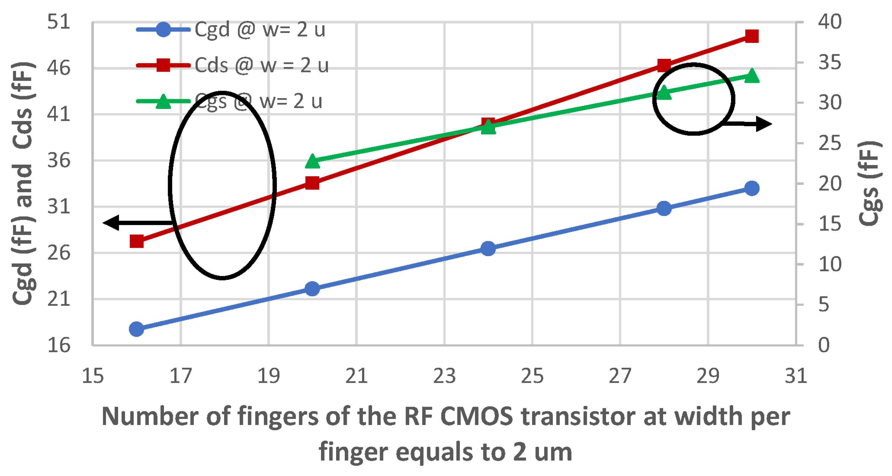
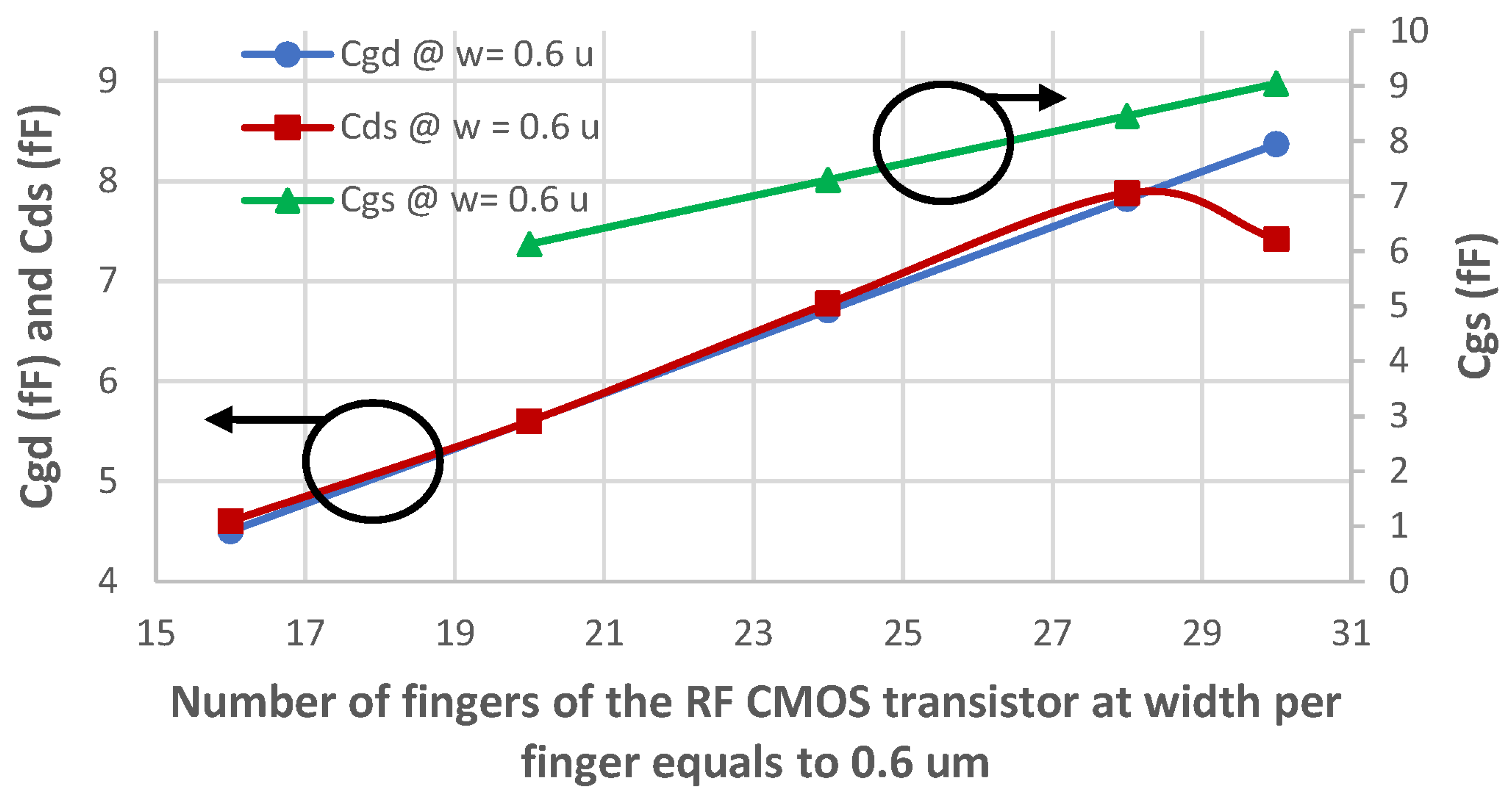
3.1. Parasitic Device Model Generator
3.2. Knowledge-Aware Simulation-Based Optimizer
3.2.1. Design Specifications Trade-Offs
3.2.2. Knowledge-Aware Simulation-Based Optimization Flow
- The user enters the required specifications with their weighting factors through the web GUI, while initial design parameters are available within the tool.
- The spice simulator generates the schematic inclusive netlist from virtuoso and the parasitic device model generator.
- The optimizer starts its optimization algorithm (BFGS) guided by the weighting factors entered by the user to know which design specification to meet first.
- Firstly, it checks on the transistors’ regions making sure that transistors are in their correct region. If this check fails, the optimizer will sweep on the transistor’s sizes and the dc current source till it passes. Every optimization loop will be on a more confined range for the concerned design parameters.
- The optimizer then simulates all the specifications giving a message indicating which specification passes and which fails.
- Depending on the weighting factor optimization methodology, the optimizer chooses which specification to meet first. Following table II, shown below, the optimizer will enter the right step stage and thereby sweeps on the parameters in favor of the specified specification.
- Repeat steps 4 to 6 till all the targeted specifications are achieved.
- Finally, the tool displays the optimized parameters, the achieved specifications, the circuit schematic, and the template of the layout with the GDSII file for further modification.
4. Verification and Simulation Results
Simulation Results
5. Conclusions
Author Contributions
Funding
Data Availability Statement
Acknowledgments
Conflicts of Interest
References
- Tsai, J.-H.; Lin, C.-L. A 40-GHz 4-Bit Digitally Controlled VGA with Low Phase Variation Using 65-nm CMOS Process. IEEE Microw. Wirel. Compon. Lett. 2019, 29, 729–732. [Google Scholar] [CrossRef]
- Jangkrajarng, N.; Zhang, L.; Bhattacharya, S.; Kohagen, N.; Shi, C.R. Template-Based Parasitic-Aware Optimization and Retargeting of Analog and RF Integrated Circuit Layouts. In Proceedings of the 2006 IEEE/ACM International Conference on Computer Aided Design, San Jose, AC, USA, 5–9 November 2006; pp. 342–348. [Google Scholar] [CrossRef]
- Carley, R.; Gielen, G.; Rutenbar, R.; Sansen, W. Synthesis tools for mixed-signal ICs: Progress on frontend and backend strategies. In Proceedings of the 33rd Annual Design Automation Conference, Las Vegas, NM, USA, 3–7 June 1996; pp. 298–303. [Google Scholar]
- Ranjan, M.; Bhaduri, A.; Verhaegen, W.; Mukherjee, B.; Vemuri, R.; Gielen, G.; Pacelli, A. Use of Symbolic Performance Models in Layout-Inclusive RF Low Noise Amplifier Synthesis. In Proceedings of the 2004 IEEE International Behavioral Modeling and Simulation Conference, San Jose, CA, USA, 22 October 2004; pp. 130–134. [Google Scholar]
- Afacan, E.; Dündar, G. A Mixed Domain Sizing Approach for RF Circuit Synthesis. In Proceedings of the 2016 IEEE 19th International Symposium on Design and Diagnostics of Electronic Circuits & Systems (DDECS), Kosice, Slovakia, 20–22 April 2016; pp. 1–4. [Google Scholar]
- Gupta, R.; Allstot, D.J. Parasitic-aware design and optimization of CMOS RF integrated circuits. In Proceedings of the 1998 IEEE Radio Frequency Integrated Circuits (RFIC) Symposium, Digest of Papers (Cat. No.98CH36182), Baltimore, MD, USA, 7–12 June 1998; pp. 325–328. [Google Scholar] [CrossRef]
- Liao, T.; Zhang, L. Parasitic-Aware GP-Based Many-Objective Sizing Methodology for Analog and RF Integrated Circuits. In Proceedings of the 2017 22nd Asia and South Pacific Design Automation Conference (ASP-DAC), Chiba, Japan, 16–19 January 2017; pp. 475–480. [Google Scholar]
- González-Echevarría, R.; Roca, E.; Castro-López, R.; Fernández, F.V.; Sieiro, J.; López-Villegas, J.M.; Vidal, N. An Automated Design Methodology of RF Circuits by Using Pareto-Optimal Fronts of EM-Simulated Inductors. IEEE Trans. Comput.-Aided Des. Integr. Circuits Syst. 2017, 36, 15–26. [Google Scholar] [CrossRef]
- González-Echevarría, R.; Castro-Lopez, R.; Roca, E.; Fernandez, F.V.; Sieiro, J.; Vidal, N.; López-Villegas, J.M. Automated Generation of the Optimal Performance Trade-Offs of Integrated Inductors. IEEE Trans. Comput.-Aided Des. Integr. Circuits Syst. 2014, 33, 1269–1273. [Google Scholar] [CrossRef]
- Martins, R.; Lourenco, N.; Passos, F.; Povoa, R.; Canelas, A.; Roca, E.; Castro-Lopez, R.; Sieiro, J.; Fernandez, F.V.; Horta, N. Two-Step RF IC Block Synthesis with Preoptimized Inductors and Full Layout Generation in-the-Loop. IEEE Trans. Comput.-Aided Des. Integr. Circuits Syst. 2019, 38, 989–1002. [Google Scholar] [CrossRef]
- Liu, B.; Deferm, N.; Zhao, D.; Reynaert, P.; Gielen, G.G. An Efficient High-Frequency Linear RF Amplifier Synthesis Method Based on Evolutionary Computation and Machine Learning Techniques. IEEE Trans. Comput.-Aided Des. Integr. Circuits Syst. 2012, 31, 981–993. [Google Scholar] [CrossRef]
- De Ranter, C.R.; Van der Plas, G.; Steyaert, M.S.; Gielen, G.G.; Sansen, W.M. CYCLONE: Automated Design and Layout of RF LCOscillators. IEEE Trans. Comput.-Aided Des. Integr. Circuits Syst. 2002, 21, 1161–1170. [Google Scholar] [CrossRef]
- Ellinger, F.; Jackel, H. Low-cost BiCMOS variable gain LNA at Kuband with ultra-low power consumption. IEEE Trans. Microw. Theory Technol. 2004, 52, 702–708. [Google Scholar] [CrossRef]
- Lo, P.-H.; Lin, C.-C.; Kuo, H.-C.; Chuang, H.-R. A Ka-band CMOS low-phase-variation variable gain amplifier with good matching capacity. In Proceedings of the 2012 9th European Radar Conference, Amsterdam, The Netherlands, 31 October–2 November 2012; pp. 532–535. [Google Scholar]
- Natarajan, A.; Nicolson, S.; Tsai, M.-D.; Floyd, B. A 60 GHz variable-gain LNA in 65 nm CMOS. In Proceedings of the 2008 IEEE Asian Solid-State Circuits Conference, Fukuoka, Japan, 3–5 November 2008; pp. 117–120. [Google Scholar]
- AnsariK, K.T.; Ross, T.; Repeta, M. An E-band variable-gain Amplifier using a programmable attenuator. In Proceedings of the European Microwave Conference (EuMC), Madrid, Spain, 23–25 September 2018; pp. 321–324. [Google Scholar]
- Ben Yishay, R.; Katz, O.; Sheinman, B.; Elad, D. High Performance E-Band Variable Gain LNA with Image Reject Filter. In Proceedings of the IEEE Asia-Pacific Microwave Conference (APMC), Singapore, 10–13 December 2019; pp. 1375–1377. [Google Scholar]
- Siao, D.S.; Kao, J.-C.; Wang, H. A 60 GHz low phase variation variable gain amplifier in 65 nm CMOS. IEEE Microw. Wirel. Compon. Lett. 2014, 24, 457–459. [Google Scholar] [CrossRef]
- Min, B.; Rebeiz, G.M. Ka-band SiGe HBT low phase imbalance differential 3-bit variable gain LNA. IEEE Microw. Wirel. Compon. Lett. 2008, 18, 272–274. [Google Scholar] [CrossRef]
- Kang, D.-W.; Kim, J.-G.; Min, B.-W.; Rebeiz, G.M. Single and four-element Ka-band transmit/receive phased-array silicon RFICs with 5-bit amplitude and phase control. IEEE Trans. Microw. Theory Tech. 2009, 57, 3534–3543. [Google Scholar] [CrossRef]
- Yi, Y.; Zhao, D.; You, X. A Ka-band CMOS digital controlled phase-invariant variable gain amplifier with 4-bit tuning range and 0.5-dB resolution. In Proceedings of the 2018 IEEE Radio Frequency Integrated Circuits Symposium (RFIC), Philadelphia, PA, USA, 10–12 June 2018; pp. 152–155. [Google Scholar]
- Shin, G.; Kim, K.; Lee, K.; Jeong, H.-H.; Song, H.-J. An E-Band 21-dB Variable-Gain Amplifier with 0.5-V Supply in 40-nm CMOS. Electronics 2021, 10, 804. [Google Scholar] [CrossRef]
- Nikandish, G.; Yousefi, A.; Medi, A. Stability analysis of broadband cascode amplifiers in the presence of inductive parasitic components. IET Circuits Devices Syst. 2014, 8, 469–477. [Google Scholar] [CrossRef]
- Brownlee, J. A Gentle Introduction to the BFGS Optimization Algorithm. Tutorial on Optimization. Available online: https://machinelearningmastery.com/bfgs-optimization-in-python/ (accessed on 19 May 2021).


| Controlling Parameters | Specifications | |||
|---|---|---|---|---|
| Gain Step | Phase Variation | Stability | Linearity | |
| Controlling transistors sizes (Wcontrolling) | ✓ | |||
| Output matching network (Co, Lct, Lo1, and Lop) | ✓ | ✓ | ✓ | |
| Interstage inductor (Lint) | ✓ | |||
| Transistor sizing (Wm and Wc) | ✓ | ✓ | ||
| RC—feedback network (CF and RF) | ✓ | |||
| Source degenerated inductor (Ls) | ✓ | ✓ | ||
| DC source (Idc) | ✓ | ✓ | ||
| Steps | Targeted Specification | Parameters to Be Optimized |
|---|---|---|
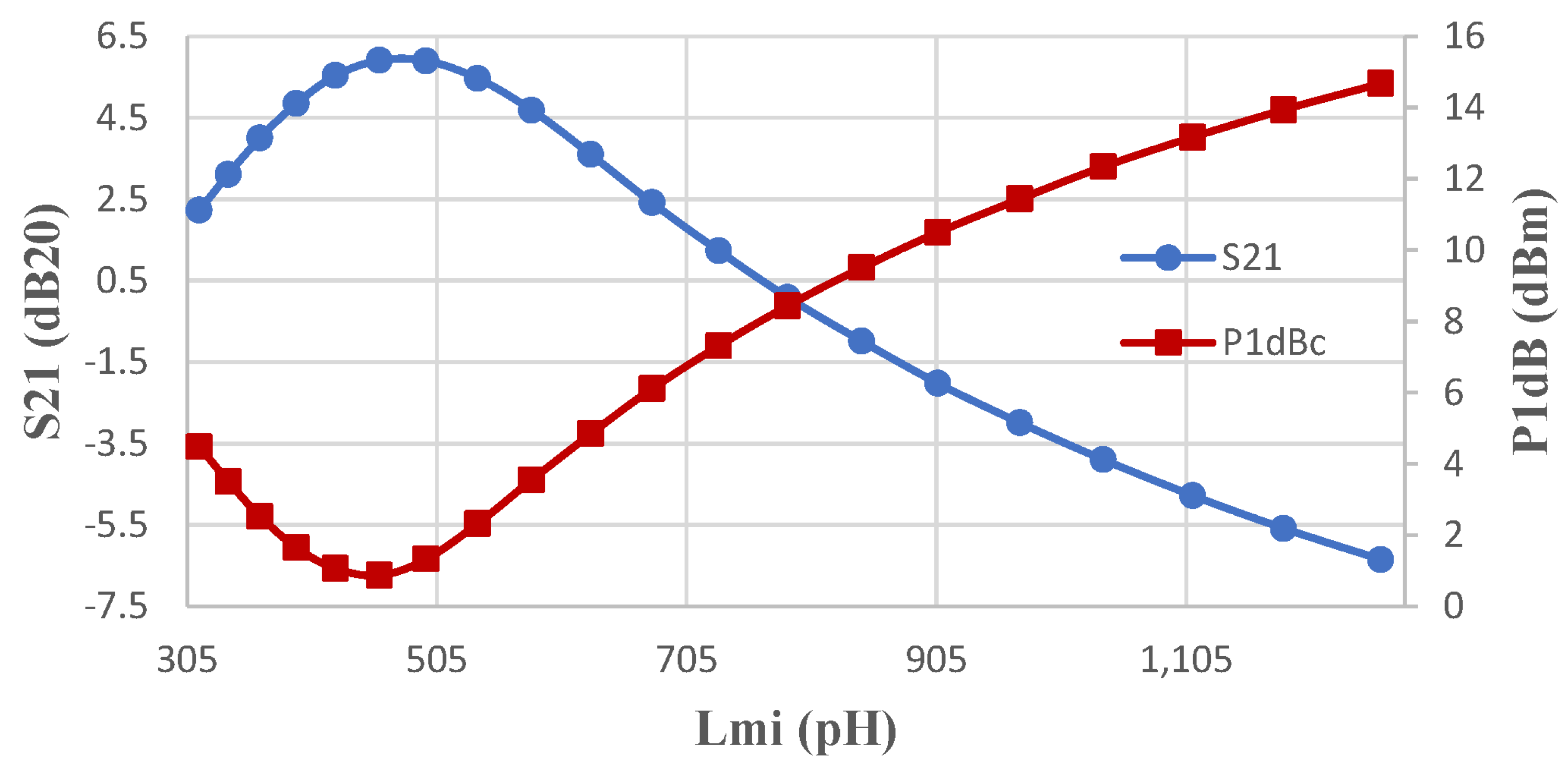
| 1 | S11 | I/P matching network elements (Lmi, Cin, Cms, and Cml) |
| 2 | S21 | I/P matching network elements (Lmi, Cin, Cms, and Cml) and O/P matching network elements (Lo, Lo1, Lop, Co, and Cop) |
| 3 | Gain Step and RMS gain error | Sizing of the controlling transistors (Wcon) |
| 4 | RMS Phase error | Interstage inductor (Lint) and O/P matching network elements (Lo, Lo1, Lop, Co, and Cop) |
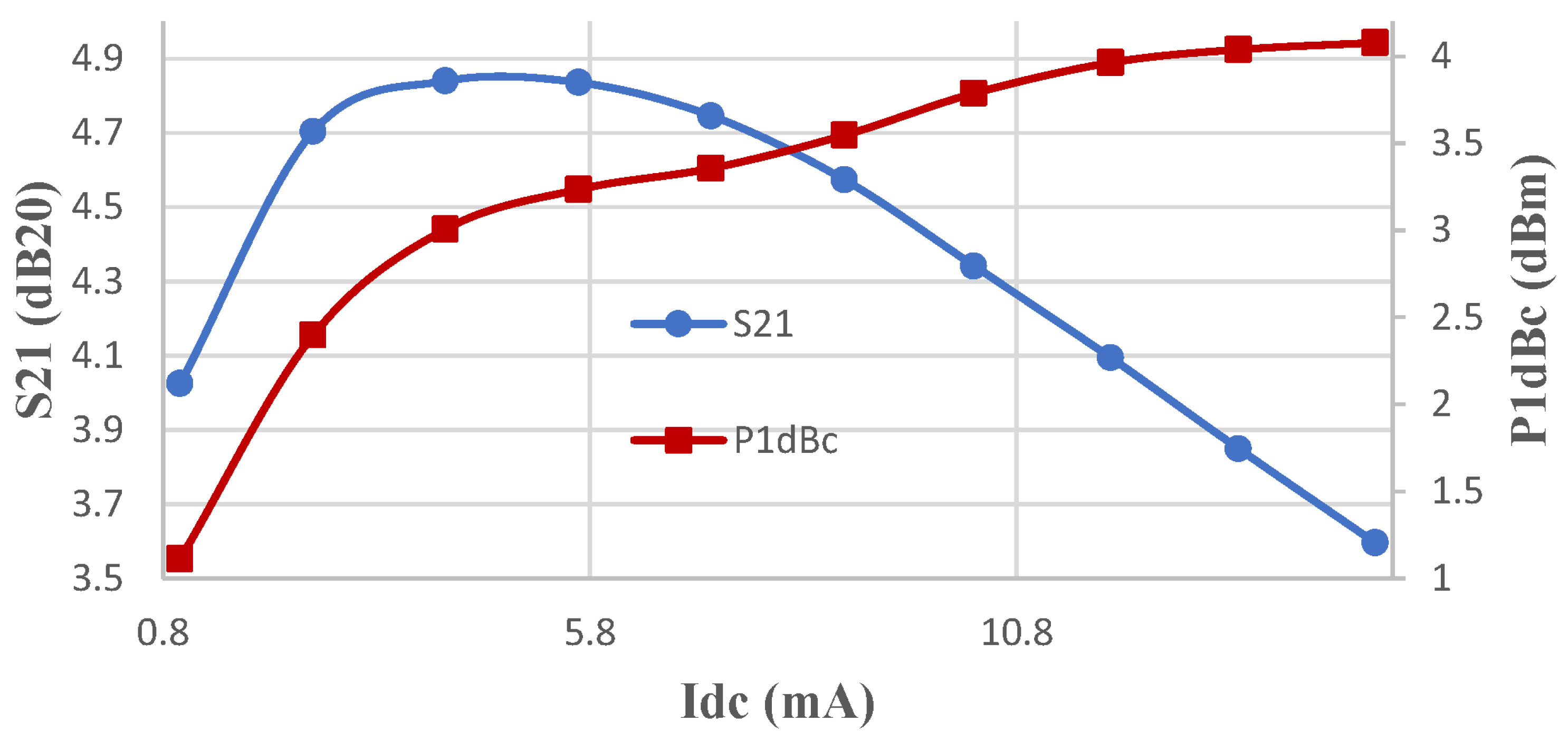
| 5 | Linearity (IP1dBc and IIP3) | Source degenerated inductor (Ls), Transistor sizing (Wm), Idc, and O/P matching network elements (Lo, Lo1, Lop, Co, and Cop) |
| 6 | Stability and Bandwidth realization | F.B. RC network elements (Rcas and Ccas) and the inductor of the output matching network (Lo1) |
| Input Matching Network | Output Matching Network | Intermediate Inductance | |||
|---|---|---|---|---|---|
| Cin (fF) | 850 | Lct (pH) | 600 | Lint (pH) | 700 |
| Cml (fF) | 700 | Lo1 (pH) | 600 | Cascode RC network | |
| Cms (fF) | 700 | Lop (pH) | 600 | Rcas (KΩ) | 10 |
| Lmi (pH) | 400 | Cmo (fF) | 400 | Ccas (fF) | 80 |
| Channel width for RF CMOS transistors | Feedback network | ||||
| Wm = Wc =Wp (um) | 2 | Ncon3 = Np3 | 8 | RF (KΩ) | 1 |
| Wcon (nm) | 600 | Ncon4 = Np4 | 4 | CF (fF) | 80 |
| Nm = Nc | 32 | Mm | 2 | Source degenerated inductance | |
| Ncon1 = Np1 | 32 | Mc | 1 | Ls (pH) | 300 |
| Ncon2 = Np2 | 16 | Mcon | 1 | ||
| Specifications | Required Specifications at 7 GHz | Achieved Specifications at 7 GHz | Required Specifications at 10 GHz | Achieved Specifications at 10 GHz | Required Specifications at 13 GHz | Achieved Specifications at 13 GHz |
|---|---|---|---|---|---|---|
| S11Frf | <−7 dB | −8 dB | <−7 dB | −14.11 dB | <−7 dB | −12.05 dB |
| S21max | >5 dB | 6.64 dB | >5 dB | 7.2 dB | >5 dB | 7.11 dB |
| IP1dBmin | >−3 dBm | 5.2 dBm | >−3 dBm | 0.83 dBm | >−3 dBm | 3.7 dBm |
| Bandwidth-min | 3 GHz | 3 GHz | 1.5 GHz | 1.7 GHz | 3 GHz | 4 GHz |
| Phase Variation | (−5°)–5° | −5° | (−5°)–5° | 4.49° | (−5°)–5° | 3.295° |
| Gain Step | 0.3 dB | 0.2581 dB | 0.5 dB | 0.417 dB | 0.4 dB | 0.3367 dB |
| IIP3 | >3 dB | 12.67 dBm | >3 dB | 8.6 dBm | >3 dB | 11.95 dBm |
| RMS Gain Error | 0.1–0.2 | 0.05 | 0.2–0.3 | 0.085 | 0.1–0.3 | 0.035 |
| RMS Phase Error | 0.2°–0.3° | 0.34° | 0.2°–0.3° | 0.26° | 0.4°–0.6° | 0.6° |
Disclaimer/Publisher’s Note: The statements, opinions and data contained in all publications are solely those of the individual author(s) and contributor(s) and not of MDPI and/or the editor(s). MDPI and/or the editor(s) disclaim responsibility for any injury to people or property resulting from any ideas, methods, instructions or products referred to in the content. |
© 2022 by the authors. Licensee MDPI, Basel, Switzerland. This article is an open access article distributed under the terms and conditions of the Creative Commons Attribution (CC BY) license (https://creativecommons.org/licenses/by/4.0/).
Share and Cite
Mansour, N.; Elnozahi, M.; Ragaai, H. Parasitic-Aware Simulation-Based Optimization Design Tool for Current Steering VGAs. Electronics 2023, 12, 132. https://doi.org/10.3390/electronics12010132
Mansour N, Elnozahi M, Ragaai H. Parasitic-Aware Simulation-Based Optimization Design Tool for Current Steering VGAs. Electronics. 2023; 12(1):132. https://doi.org/10.3390/electronics12010132
Chicago/Turabian StyleMansour, Nehad, Mohamed Elnozahi, and Hani Ragaai. 2023. "Parasitic-Aware Simulation-Based Optimization Design Tool for Current Steering VGAs" Electronics 12, no. 1: 132. https://doi.org/10.3390/electronics12010132
APA StyleMansour, N., Elnozahi, M., & Ragaai, H. (2023). Parasitic-Aware Simulation-Based Optimization Design Tool for Current Steering VGAs. Electronics, 12(1), 132. https://doi.org/10.3390/electronics12010132