Communication

A Figure of Merit for Selection of the Best Family of SiC Power MOSFETs

1
Queensland Micro- and Nanotechnology Centre, Griffith University, Brisbane, QLD 4111, Australia
2
Department of Electronics and Communication Engineering, Graphic Era (Deemed to be University), Dehradun 248002, India
*
Author to whom correspondence should be addressed.
Electronics 2022, 11(9), 1433; https://doi.org/10.3390/electronics11091433
Submission received: 13 April 2022 / Revised: 27 April 2022 / Accepted: 28 April 2022 / Published: 29 April 2022
(This article belongs to the Section Semiconductor Devices)

Abstract

:
This paper proposes a criterion to select the best family of commercial SiC power metal–oxide–semiconductor field-effect transistors (MOSFETs) that provides the highest quality and reliability. Applying a recently published integrated-charge method, a newly proposed figure of merit is correlated to the density of near-interface traps that degrade the quality and reliability of SiC MOSFETs. The applicability of the proposed figure of merit is experimentally demonstrated with the most widely used and commercially available planar and trench MOSFETs from different manufacturers.

1. Introduction

Power semiconductor devices are key components of advanced power conversion systems. The SiC metal–oxide–semiconductor field-effect transistors (MOSFETs) are now available commercially and contribute towards the development of power-conversion systems with a reduced size and reduced power losses. Compared to silicon, SiC permits the use of much higher doping concentrations and thinner drift layers for a given blocking voltage [1,2]. This results in a much smaller on-resistance, R D S ( o n ) [3]. Moreover, continued effort by the industry to improve the performance and reliability results in modified processes and device structures for the case of both planar and trench MOSFETs.
Despite all of the advancements, oxide defects near the SiO 2 /SiC interface continue to degrade the quality and reliability of SiC MOSFETs [4]. These defects act as near-interface traps (NITs) that capture and release electrons, creating both performance and reliability issues [5,6,7]. At sub-threshold voltages, the NITs energetically located below the conduction band capture electrons and appear as fixed charge that increases the threshold voltage. The density of these NITs can increase during device operation, which degrades the reliability of the device [8,9]. However, when the gate voltage is increased above the threshold voltage, the quantum confinement effect sets the Fermi level inside the conduction band. In that case, the NITs with energy levels aligned to the Fermi level inside the conduction band constantly capture and release electrons from the MOSFET channel. This drops the effective mobility of channel carriers from a trap-free level of around 200 cm 2 /Vs down to around 30–40 cm 2 /Vs, because—on average—more than 80% of electrons attracted by the gate voltage can be trapped by NITs at any instant of time [7,10,11]. This reduction in the effective channel-carrier mobility increases the on-resistance of the MOSFET [12,13].
The on-resistance can be reduced by increasing the effective channel width of the MOSFET, but this will increase the output capacitance, which will cause an increase in the dynamic power dissipation, which becomes increasingly important as the switching frequency is increased. However, if a specific technology process or device structure—such as planar or trench MOSFETs—reduces the density of near-interface traps ( N N I T ), the quality and reliability of all MOSFETs in this family will be higher.
Every manufacturer provides several device parameters in their datasheets of the device. Even then, various other device parameters that are not provided in the datasheets have a significant impact on the quality and reliability of MOSFETs. As a result of that, circuit designers are unable to select the best family of MOSFETs and then decide on a specific MOSFET from that family, based on the values of the on-resistance and output capacitance that would minimize the power dissipation in their circuits.
In this paper, we propose a simple criterion to select the best family of MOSFETs. Using our recently published method [7,14] for the measurement of the density of near-interface traps in commercial MOSFETs, we demonstrate in the paper that the simple criterion ensures the selection of the commercially available MOSFET family with the lowest density of NITs and, therefore, the highest quality and reliability.

2. Theory

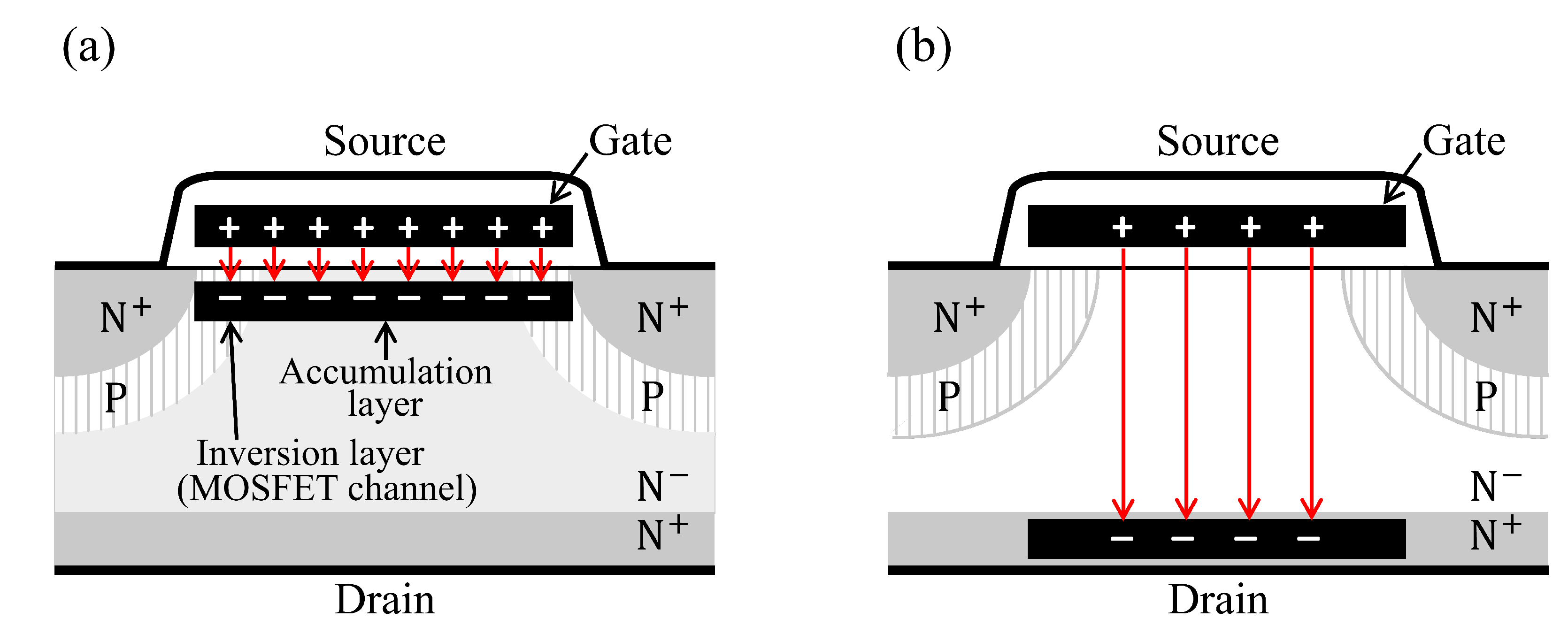
2.1. Dependence of on-Resistance on the Density of near Interface Traps

The constant endeavor of the semiconductor industry is to minimize the power dissipation and increase the current handling capability by reducing R D S ( o n ) through improvements in the manufacturing process [15]. However, there exists a high density of NITs at the SiO 2 /SiC interface of the SiC MOSFETs [13,16]. These NITs trap electrons from the channel and reduce the effective channel-carrier mobility of the device [14]. This reduction in mobility increases the channel resistance ( R C H ) and consequently increases the R D S ( o n ) of the MOSFET [17,18].

2.2. The Figure of Merit for Selection/Comparison of SiC MOSFET Families

The width of the channel (W) is a critical parameter that is not available in the power MOSFET datasheets. It is a well known fact that the R D S ( o n ) of the power MOSFET is inversely proportional to W [16,17,19]. Accordingly, MOSFETs with different R D S ( o n ) values that are in a single family have different W values, whereas all other technological parameters are the same. In power MOSFETs, W is proportional to the gate area and, consequently, the gate-capacitance ( C G ) of the device is directly proportional to W [16,17]. Multiplying R D S ( o n ) and C G results in a quantity that is independent of W:
R D S ( o n ) × C G = κ
Due to the fact that the constant κ groups all of the technical parameters of a particular MOSFET family, it can be considered as a figure of merit for that family of MOSFETs.
The proposed constant κ is different from Baliga’s figure of merit [16], defined as R D S ( o n ) × Q G D , where Q G D is the charge at the gate-to-drain capacitance ( C G D ) at the maximum drain-to-source voltage when the MOSFET is turned off ( V G S = 0 ). In Baliga’s figure of merit, Q G D and C G D relate to the dynamic power dissipation, whereas C G in the proposed figure of merit is measured at V D S = 0 and, therefore, is unrelated to the dynamic power dissipation. The proposed figure of merit relates to the performance and reliability affected by NITs, which is different from optimizing dynamic and static power dissipation.
The R D S ( o n ) is available in the datasheet of every MOSFET and only C G needs to be measured at the operating gate voltage ( V G ) to obtain the value of κ .

3. Experimental Demonstration

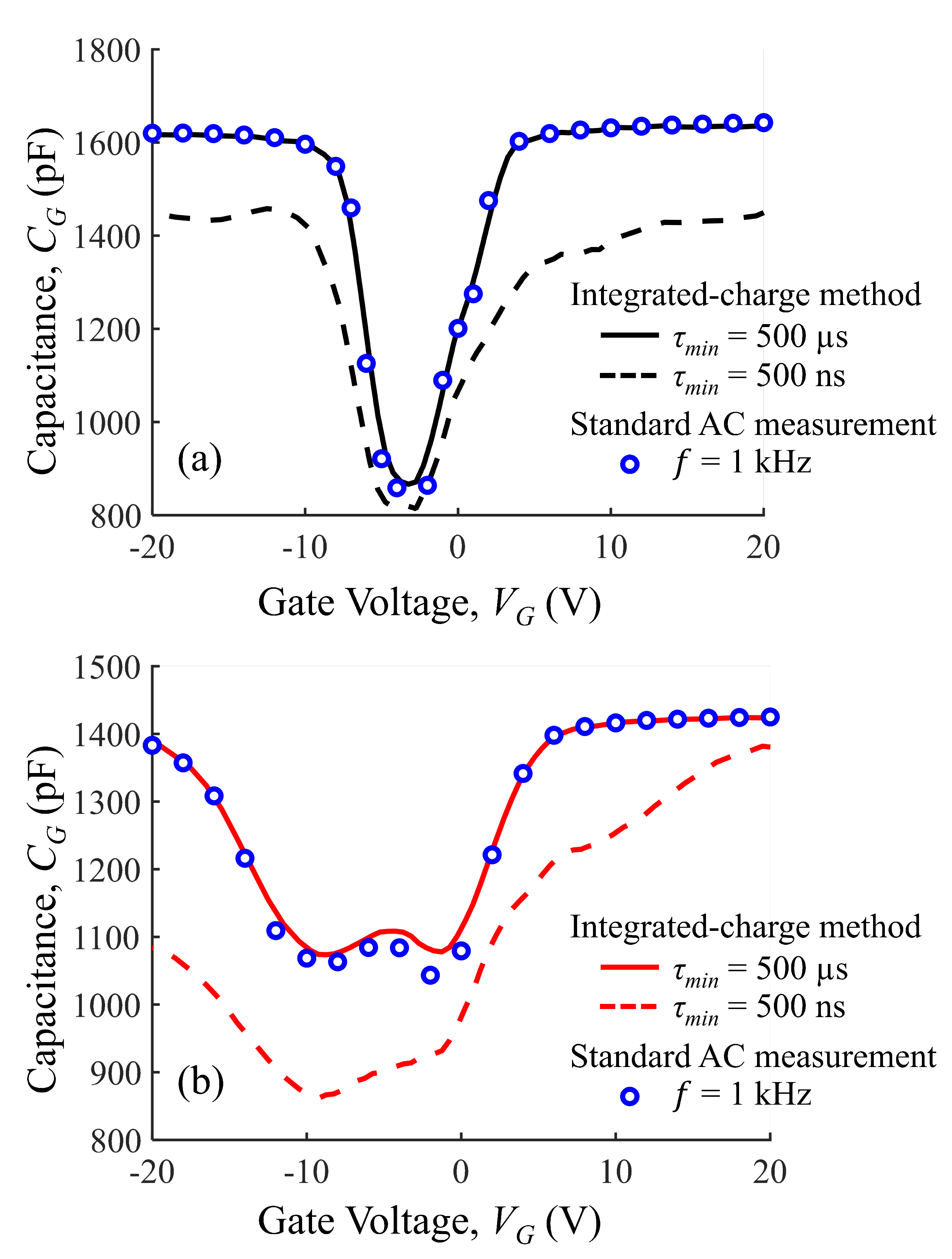
3.1. Measurement of Gate Capacitance and On-Resistance

In this paper, we used 1200 V commercial N-channel SiC power MOSFETs manufactured by different manufacturers, with the parameters listed in Table 1. The R D S ( o n ) was determined using standard I–V measurements provided in the datasheets by the manufacturers.
For C G at the operating V G , the C–V measurements were conducted with the source and drain terminals grounded. The C G can be given by:
C G = C G S + C G D
where C G S is the gate-to-source capacitance and C G D is the gate-to-drain capacitance of the MOSFET at the operating gate voltage. It is important to note that C G is different from the input capacitance ( C i s s ) given in the datasheets. The datasheets provide C i s s at zero gate voltage, rather than the operating V G , and large drain-to-source voltages ( V D S ) that deplete the drift region under the gate. Both C G and C i s s are directly proportional to W, but C G is inversely proportional to the gate-oxide thickness, whereas C i s s is inversely proportional to the depletion layer width, which can be different in different device structures [17].
Figure 1a shows the cross-section of a power MOSFET with a planar gate structure to illustrate that the capacitance C G at the operating gate voltage and V D S = 0. It can be observed that the MOSFET channel of electrons is created by the inversion of the P-type body at the semiconductor surface. Meanwhile, the drift region forms an accumulation layer, which means that the active area of the capacitance is equal to the gate area, A G . The capacitance C i s s at zero gate bias is illustrated in Figure 1b. As a result of small V G and large V D S values, the drift region under the gate is depleted. This creates a much thicker dielectric and, consequently, C i s s is much lower than C G .
Since most of the manufacturers provide R D S ( o n ) at V G = 18 V, C G was measured at V G = 18 V to obtain the values of κ . The circuit designers can measure C G at V G = 18 V with standard AC measurements at 1 kHz, using any commercial instrument, such as Agilent or Keithley. However, it is important to note that the standard AC measurements at high frequencies (≥100 kHz) are not reliable because the high density of fast NITs distort the sinusoidal waveforms [17,20]. The issue with this distortion is that the AC method of capacitance measurements assumes undistorted sinusoidal signals.

3.2. Measurement of the Density of Near-Interface Traps

Trapped channel electrons by NITs do not contribute to the MOSFET current, which results in higher R D S ( o n ) when the density of NITs is higher [17]. Given that the gate capacitance C G is a constant determined by the thickness of the gate oxide and the gate area, the value of κ is also directly proportional to the density of NITs. In this section, we present an experimental demonstration that smaller values of κ correspond to lower densities of NITs. The purpose is to justify the use of κ as a figure of merit in terms of quality and reliability.
Measurement of the density of NITs ( N N I T ) in commercial MOSFETs is possible by applying our recently published integrated-charge method [7,14]. This method can detect NITs with response times between 500 ns and 500 μ s.
To apply the integrated-charge method to a MOSFET, the drain and the source were connected to the ground and an external resistance R E X T was connected to the gate. The series R C circuit was biased with a DC voltage, whose value was changed from +20 V to −20 V. At a set DC voltage, small voltage steps ( Δ V s t e p ) of a variable step interval ( t s t e p ) were superimposed to the DC voltage in the form of a pulse waveform with the frequency f = 1 / 2 t s t e p . A Tektronix DPO 7104 oscilloscope with Tektronix P6139B voltage probes was used to measure the voltage across the R E X T , and, in that way, to determine both the current charging the gate capacitance during t s t e p = 1 / 2 f when Δ V s t e p is applied and the current discharging the capacitor during t s t e p = 1 / 2 f when the pulse is removed. The charging and discharging currents are integrated to obtain the charge q Δ N c a r r i e r s in response to the applied voltage step. This charge corresponds to an apparent or electrically active gate capacitance C G = q Δ N c a r r i e r s Δ V s t e p .
Figure 2 shows the C–V curves obtained using the integrated-charge method and the standard AC measurement for both planar and trench MOSFETs from manufacturer D. All of the experiments were performed at room temperature. The integrated-charge measurements were performed with step intervals of 500 μ s and 500 ns. The standard AC measurements were performed at 1 kHz using an Agilent B1505A Power Device Analyzer. The purpose of showing a standard AC measurement at 1 kHz is to demonstrate that C G at V G = 18 V, needed to determine the value of κ in (1), can be obtained either by commercial instruments or by the integrated-charge method.
It can be observed from Figure 2 that there is a reduction in the apparent capacitance when the measurements were performed with the shorter step interval. This is because the trapped charge with response times longer than τ m i n = t s t e p does not contribute to the charging and discharging current. As a result, the integrated charge q Δ N c a r r i e r s is smaller and so is the apparent capacitance. Therefore, the density of trapped carriers per unit area with response times longer than 500 ns and shorter than 500 μ s is equal to:
Δ N t r a p p e d = Δ N c a r r i e r s ( 500 μ s ) Δ N c a r r i e r s ( 500 ns ) A G
where A G is the gate area.
Given that the typical value of the gate-oxide thickness in commercial MOSFETs is 50 nm [7,21], A G was determined from the measured C G at V G = 18 V. The step interval of 500 μ s was selected as the reference because the trap density with a response time longer than 500 µs was too small to be detected.
The C–V curves in Figure 2 show that there is a trapping of electrons for positive gate voltages and trapping of holes for negative gate voltages. Since the trapping of holes does not impact the channel resistance, the trapping of electrons is considered for the calculation of the relevant N N I T . The total density of trapped electrons at the relevant near-interface traps at a given V G can be calculated as:
N N I T = 0 V G Δ N t r a p p e d

4. Application to Commercial Devices

We measured 1200 V commercial SiC power MOSFETs with both planar and trench structures. The R D S ( o n ) and C G at V G = 18 V for all the MOSFETs are listed in Table 1. The density of NITs at V G = 18 V, measured for each MOSFET, and the corresponding figure of merit, κ , are shown in Figure 3. The planar MOSFETs are represented by the squares, whereas the trench MOSFETs are shown with circles. These results verify the theory that the figure of merit ( κ ) is proportional to the density of near-interface traps ( N N I T ). The difference in N N I T in different families of MOSFETs is six times, which represents a significant difference between different manufacturers. This leads to the difference in the figure of merit of five times, which is due to the dominant impact of near-interface traps on R D S ( o n ) . Different manufacturers apply different processes for the gate dielectric, but the proposed method is applicable to these different dielectrics because N N I T , as the ultimate result of these processes, is the quantity that directly impacts R D S ( o n ) and the figure of merit.
Figure 3 also shows that the trench MOSFETs are better in comparison to the planar MOSFETs. This result may be surprising, but it is consistent with the higher channel-carrier mobility that is commonly observed in trench SiC MOSFETs.
It is important to note that the values of C G obtained by the standard AC measurements at 1 kHz, along with the values of R D S ( o n ) available in the datasheets, are sufficient to determine the values of κ by (1). This enables circuit designers to compare SiC MOSFET families and to select the MOSFET family with the lowest value of κ . This will ensure the lowest density of NITs and, hence, the best quality and reliability.

5. Conclusions

This brief proposes a figure of merit, κ , as a criterion for the selection of the best family of SiC power MOSFETs. The applicability of the proposed figure of merit was experimentally demonstrated for two gate structures—planar and trench—from five manufacturers. The values of κ can easily be calculated using R D S ( o n ) given in the MOSFET datasheets and a standard measurement of gate capacitance. The proposed figure of merit will enable power engineers to select the best MOSFET family in the first instance, and then to select a specific MOSFET from this family with the specific values of R D S ( o n ) and output capacitance that minimize the sum of static and dynamic power dissipation in the designed circuit.

Author Contributions

Conceptualization, M.C. and S.D.; methodology, M.C. and S.D.; experimental investigation, M.C. and S.D.; software, M.C; data curation, M.C.; data analysis and discussion, M.C., S.D., D.H., H.A.M., P.P. and U.J.; writing—original draft, M.C. and S.D.; writing—review and editing, M.C., S.D. and D.H.; supervision, S.D. and H.A.M.; project administration, S.D. and H.A.M. All authors have read and agreed to the published version of the manuscript.

Funding

This work was performed at the Australia National Fabrication Facility (ANFF), Queensland node, QLD, Australia, a company established under the National Collaboration Research Infrastructure Strategy to provide nano- and microfabrication facilities to Australia’s researchers.

Data Availability Statement

Data are contained within the article.

Conflicts of Interest

The authors declare no conflict of interest.

References

  1. Hazra, S.; De, A.; Cheng, L.; Palmour, J.; Schupbach, M.; Hull, B.A.; Allen, S.; Bhattacharya, S. High Switching Performance of 1700-V, 50 A SiC Power MOSFET Over Si IGBT/BiMOSFET for Advanced Power Conversion Applications. IEEE Trans. Power Electron. 2016, 31, 4742–4754. [Google Scholar]
  2. Dimitrijev, S.; Han, J.; Moghadam, H.A.; Aminbeidokhti, A. Power-switching Applications beyond Silicon: Status and Future Prospects of SiC and GaN Devices. MRS Bull. 2015, 40, 399–405. [Google Scholar] [CrossRef]
  3. Li, S.; Lu, S.; Mi, C.C. Revolution of Electric Vehicle Charging Technologies Accelerated by Wide Bandgap Devices. Proc. IEEE 2021, 109, 985–1003. [Google Scholar] [CrossRef]
  4. Kimoto, T.; Watanabe, H. Defect Engineering in SiC Technology for High-Voltage Power Devices. Appl. Phys. Exp. 2020, 13, 399–405. [Google Scholar] [CrossRef]
  5. Fiorenza, P.; Giannazzo, F.; Roccaforte, F. Characterization of SiO2/4H-SiC Interfaces in 4H-SiC MOSFETs: A Review. Energies 2019, 12, 2310. [Google Scholar] [CrossRef] [Green Version]
  6. Pande, P.; Haasmann, D.; Han, J.; Moghadam, H.A.; Tanner, P.; Dimitrijev, S. Electrical Characterization of SiC MOS Capacitors: A Critical Review. Microelectron. Reliab. 2020, 112, 113790. [Google Scholar] [CrossRef]
  7. Chaturvedi, M.; Dimitrijev, S.; Haasmann, D.; Moghadam, H.A.; Pande, P.; Jadli, U. Quantified Density of Performance-Degrading Near-Interface Traps in SiC MOSFETs. Sci. Rep. 2022, 12, 4076. [Google Scholar] [CrossRef] [PubMed]
  8. Lelis, A.J.; Green, R.; Habersat, D.B. SiC MOSFET Threshold-Stability Issues. Mater. Sci. Semicond. Process. 2018, 78, 32–37. [Google Scholar] [CrossRef]
  9. Jiang, H.; Zhong, X.; Qiu, G.; Tang, L.; Qi, X.; Ran, L. Dynamic Gate Stress Induced Threshold Voltage Drift of Silicon Carbide MOSFET. IEEE Electron Device Lett. 2020, 41, 1284–1287. [Google Scholar] [CrossRef]
  10. Urresti, J.; Arith, F.; Olsen, S.; Wright, N.; O’Neill, A. Design and Analysis of High Mobility Enhancement-Mode 4H-SiC MOSFETs using a Thin-SiO2/Al2O3 Gate-Stack. IEEE Trans. Electron Devices 2019, 66, 1710–1716. [Google Scholar] [CrossRef] [Green Version]
  11. Tachiki, K.; Kaneko, M.; Kimoto, T. Mobility Improvement of 4H-SiC (0001) MOSFETs by a Three-Step Process of H2 Etching, SiO2 Deposition, and Interface Nitridation. Appl. Phys. Exp. 2021, 14, 031001. [Google Scholar] [CrossRef]
  12. Moghadam, H.A.; Dimitrijev, S.; Han, J.; Haasmann, D. Active Defects in MOS Devices on 4H-SiC: A Critical Review. Microelectron. Rel. 2016, 60, 1–9. [Google Scholar] [CrossRef]
  13. Pande, P.; Dimitrijev, S.; Haasmann, D.; Moghadam, H.A.; Chaturvedi, M.; Jadli, U. Impact of Nitridation on the Active Near-Interface Traps in Gate Oxides on 4H-SiC. Solid-State. Electron. 2020, 171, 107874. [Google Scholar] [CrossRef]
  14. Chaturvedi, M.; Dimitrijev, S.; Moghadam, H.A.; Haasmann, D.; Pande, P.; Jadli, U. Fast Near-Interface Traps in 4H-SiC MOS Capacitors Measured by an Integrated-Charge Method. IEEE Access 2021, 9, 109745–109753. [Google Scholar] [CrossRef]
  15. Friedrichs, P. High-Performance CoolSiC™ MOSFET Technology with Silicon-Like Reliability. Infineon Technologies. Available online: www.infineon.com (accessed on 3 January 2022).
  16. Baliga, B.J. Power MOSFETs. In Fundamentals of Power Semiconductor Devices, 2nd ed.; Springer: Raleigh, NA, USA, 2019; pp. 413–449. [Google Scholar]
  17. Dimitrijev, S. MOSFET. In Principles of Semiconductor Devices, 2nd ed.; Oxford University Press: New York, NY, USA, 2012; pp. 470–472. [Google Scholar]
  18. Pezzimenti, F.; Bencherif, H.; De Martino, G.; Dehimi, L.; Carotenuto, R.; Merenda, M.; Della Corte, F.G. Study and Assessment of Defect and Trap Effects on the Current Capabilities of a 4H-SiC-Based Power MOSFET. Electronics 2021, 10, 735. [Google Scholar] [CrossRef]
  19. Jadli, U.; Mohd-Yasin, F.; Moghadam, H.A.; Pande, P.; Chaturvedi, M.; Dimitrijev, S. A Method for Selection of Power MOSFETs to Minimize Power Dissipation. Electronics 2021, 10, 2150. [Google Scholar] [CrossRef]
  20. Pande, P.; Dimitrijev, S.; Haasmann, D.; Moghadam, H.A.; Tanner, P.; Han, J. Direct Measurement of Active Near-Interface Traps in the Strong-Accumulation Region of 4H-SiC MOS Capacitors. IEEE J. Electron Devices Soc. 2018, 6, 468–474. [Google Scholar] [CrossRef]
  21. Agarwal, A.; Han, K.; Baliga, B.J. 600 V 4H-SiC MOSFETs Fabricated in Commercial Foundry with Reduced Gate Oxide Thickness of 27 nm to Achieve IGBT-Compatible Gate Drive of 15 V. IEEE Electron Device Lett. 2019, 40, 1792–1795. [Google Scholar] [CrossRef]
Figure 1. Cross-section of a planar power MOSFET illustrating that (a) the gate capacitance ( C G ) at the operating V G and (b) the input capacitance ( C i s s ) at V G = 0 V and V D S > 0 V.
Electronics 11 01433 g001
Figure 2. Capacitance–voltage curves for the MOSFETs from manufacturer D with (a) planar gate structure; (b) trench gate structure.
Electronics 11 01433 g002
Figure 3. Comparison of 1200 V commercial power MOSFETs listed in Table 1 using the density of near-interface traps ( N N I T ) and the corresponding figure of merit ( κ ).
Electronics 11 01433 g003
Table 1. On-resistance and measured gate capacitance at V G = 18 V for 1200 V commercial power MOSFETs.
MOSFET IDManufacturerGate StructureOn-Resistance (m Ω )Gate Capacitance (pF)
A-TATrench90977
350280
B-PBPlanar281530
C2-PCPlanar360583
C3-PCPlanar282592
D-TDTrench1051424
D-PDPlanar2801635
E-PEPlanar1921295
Publisher’s Note: MDPI stays neutral with regard to jurisdictional claims in published maps and institutional affiliations.

