Abstract
This paper presents a new analog design for a radio-frequency identification (RFID) tag antenna with a long-read range oriented to localization applications. The actual work focuses on the analog input characterization of antenna impedance by studying the capacitive effect, created by the gaps, and the effect of the introduced opened circuited L-shaped stubs, on the RFID tag characteristics. Numerical and measured results confirm that proposed tag antenna performances are significantly improved by introducing gaps and stub structures and after optimizing their dimensions, such as length and width. The introduced stubs with optimum dimensions provide good impedance matching, and improved return loss values. Furthermore, two operating frequency bands have been created when the antenna is excited by a 50 Ω port: a low-frequency band around 837 MHz and a higher one around 927 MHz. These results have been validated by measured ones. The proposed RFID antenna is mainly composed of three split rectangular resonators (SRR) where introduced structures concern only the larger SRR. The optimized antenna has an area of 76 × 24.6 mm2 and is printed on the Taconic RF-60A substrate with a dielectric constant of 6.12, a thickness of 1.6 mm, and a loss tangent of 0.025. Simulation results show interesting communication performances, of the proposed tag antenna, with a return loss of −22.3 dB around 916 MHz and a long-read range up to 25 m when it is fed by an industrial Mping M730 chip with a power sensitivity of −24 dB and an output impedance Zchip = 16 − j194 (Ω) at 916 MHz
1. Introduction
Radio-Frequency Identification (RFID) has recently gained a lot of attention in different sectors due to its robust application capabilities. This technology uses electromagnetic fields to automatically identify, and track tags attached to objects or animals. Stockman [1] was one of the first to employ RFID technology in communications. In addition to communication, RFID has huge potential applications in many areas, such as transportation, manufacturing, and supply systems [2,3,4]. RFID is one of the emerging technologies being used as an alternative to overcome some of the problems associated with current identification technologies, such as barcodes and optical systems. In comparison to other techniques of identification, such as barcode, RFID tags provide better accuracy, higher read range, and easy manipulation [5]. However, the production cost is still expensive when compared to the price of the barcode.
RFID has many operating frequencies [6,7], hence, it can be classified into four major categories: low frequency (125–134 and 140–148.5 kHz), high frequency (13.56 MHz), ultra-high frequency (UHF) (865–965 MHz), and microwave RFID systems band for 2.45 GHz or 5.8 GHz [8]. RFID UHF bands include frequencies between 860 MHz and 960 MHz, which may vary depending on the country [9]. An RFID system is composed of two main components, the readers, and the transponder “tags”. This paper can be classified into two types: active tag and passive tag. As the name suggests, an active tag contains an onboard battery as a power supply, whereas a passive RFID tag works by using electromagnetic energy transmitted from an RFID reader. This latter transmits the RF power with an interrogating signal toward the tag-antenna. A fraction of this power is received by the chip, behind the RFID antenna, and reacts by varying its input impedance, which modulates the backscattered signal (Figure 1) [10].
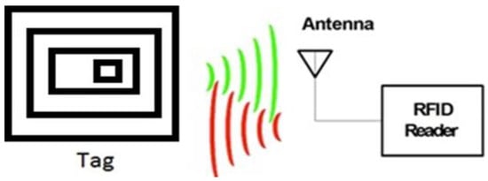
Figure 1.
RFID system: Reader and Tag communication system.
In recent years, several studies were established to enhance the performance of RFID systems. The capacitive effect created by gaps was successfully used in [11], where a novel approach for designing a parasitic Split Ring Resonator antenna was introduced. In addition to the gap method, the performance of the system depends greatly on the chip’s dimensions. In [12], a parametric study on stubs and load sizes was performed to enhance the characteristics of the proposed antenna [13].
The present work proposes a new UHF dual-band antenna design with high capabilities that combines two interesting techniques. The first technique takes advantage of the capacitive effect by creating gaps in the structure. The second technique aims to efficiently adjust antenna impedance by introducing L-shaped opened circuited stubs to enhance the performance of the proposed antenna, thereby optimally matching the chip impedance. This allows the tag to transmit more energy and then, to communicate with a reader over a long distance. One of the considered scenarios of using RFID tags for localization applications is to use the reader’s receiving antenna, attached to a moving vehicle, to detect the returned signal given by RFID tags fixed on the load. Each RFID tag can send its localization coordinates to the reader which allows the calculator to determine, in real-time, the position of the vehicle based on the transmitted RFID signal’s power.
This manuscript is organized as follows: Section 2 presents some general definitions and RFID antennas’ characteristics. Section 3 illustrates the techniques used to achieve better chip impedance matching, such as gaps and stubs, and introduces the proposed antenna structure. To evaluate the effect of each technique, a numerical study is performed in Section 4. The proposed antenna structure performances results are validated through an experimental study in Section 5. Finally, Section 6 gives the conclusions.
2. Materials and Methods
2.1. The RFID Technology
RFID belongs to a group of technologies known as Automatic Identification and Data Capture (AIDC). AIDC methods aim to automatically identify objects or persons and process various information about them with little or no human intervention. The basic form of RFID systems, Figure 1, consists of three components, which are the RFID tag, the RFID reader, and the antenna.
RFID tags are made up of an integrated circuit (IC) and an antenna that transmits information as radio waves to the RFID reader. The reader converts the radio waves into a more suitable form of data. These data are then collected and transferred to a remote system through a communications interface for storage and processing.
2.2. Chip Impedance Matching
The performance of the RFID system can be affected by several parameters and conditions. To reach the optimum operating condition, the antenna impedance should be matched correctly to the chip impedance, which is known to vary depending on the received power of the chip. Moreover, when the chip and the antenna impedance are both complex, the estimation of the power reflection coefficient for tag antenna design is complicated. In general, the chip can be modeled by an equivalent electrical circuit containing a resistance R and a capacitor C. The two components can be either in parallel or in series, as shown in Figure 2. The impedance of the equivalent electrical circuit is expressed as follows:
where . By considering that in ultra-high frequency band, Equation (1) becomes,
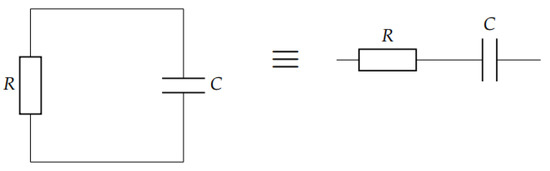
Figure 2.
Chip lumped RC circuit model.
Based on Equation (2), the real part and the imaginary part of the chip impedance depend on the frequency f. Furthermore, as the frequency increases, the real part of the impedance decreases more rapidly than its imaginary part.
2.3. The Read Range
A lower return loss remains one of the most important RFID tag characteristics because it allows for the transmittal of more electromagnetic power and, hence, achieves a longer read range. Based on the principle of the Friis transmission equation, the read range r of an RFID UHF system is expressed as follows [14]:
where Pt, Gt, Gr, and τ are, respectively, transmitted power from the reader, tag antenna gain, reader gain, and power transmission coefficient between antenna and chip. Pth is the minimum RF power required by the chip to turn on. τ can be expressed in terms of chip reflection coefficient Γ when it is playing the role of a receiver; their expressions are as follows
where,
3. Proposed Antenna Structure
3.1. Gaps and the Capacitive Effect
Based on the chip electrical model, the RFID functioning parameters, such as resonance frequency and bandwidth, are defined using resistance R and the capacitance C values. Equation (2) shows that antenna impedance is more influenced by the capacitance C than the resistance R. Thus, RFID functioning parameters depend mainly on the value of the capacity C. In practice, the capacitors require an insulator between two plates, otherwise, the charge could not remain on the plates, it would dissipate through the medium between the two plates. In our proposed structure, the capacitive effect is created by introducing gaps in the structure while air plays the role of insulator.
The gap capacitance, Cgap, which is the coupling capacitance between two metal surfaces separated by a distance L, can be expressed as [15]:
where ε0 and εr are, respectively, the vacuum permittivity and the substrate permittivity, and h is substrate thickness. The used approximation (5) works only when there is no ground plane [8].
Figure 3 presents variations of gap capacitance Cgap which depends on the gap length L and the thickness h following Equation (5). Based on these simulated results, Equation (5) is only valid, i.e., the value of Cgap is real, when the gap length, L, is lower than two times the thickness h: L < 2 h. Moreover, Cgap decreases as the gap length increases and becomes negative as h < L < 2 h. Furthermore, the negative capacitance Cgap may result in unexpected behavior that can affect the functioning parameters.
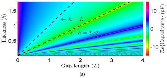
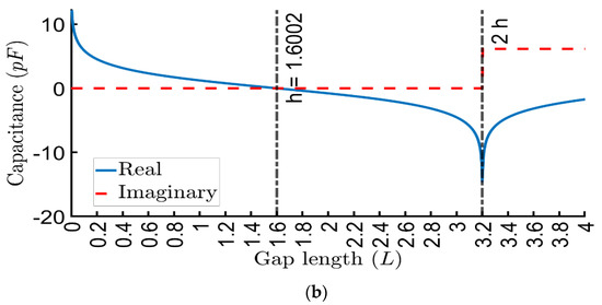
Figure 3.
The gap dimension effect on the capacity: (a) Capacity in terms of gap length and substrate thickness (L, h); (b) Capacity vs. gap length when substrate thickness h = 1.6002 mm.
3.2. Stubs
Using stubs is a well-known method for impedance matching circuits. A stub is an opened or short-circuited line of suitable length used as a reactance shunted across the transmission line, of characteristic impedance Zc, at a calculated distance from the matched load of impedance ZL. Matching stubs can be made adjustable so that matching can be corrected easily.
In practice, several antennas use stubs as part of their components. Generally, the transmission line losses are negligible, and the input impedance of the stub is considered purely reactive. This impedance depends on the stub type, which can be either an open or short circuit, and on its length. As result, stubs can behave as frequency-dependent capacitors or frequency-dependent inductors. This property makes the stubs very useful in any mechanism used for antenna impedance matching circuits as shown in Figure 4. Furthermore, a single stub will only achieve a perfect matching at a narrow frequency band while wideband matching may require several stubs spaced along the main transmission line (i.e., antenna feed line).
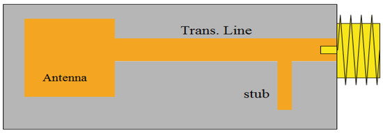
Figure 4.
Stub placed just before an output connector to compensate for small mismatches due to the connector.
3.3. Proposed Design
The proposed antenna design exploits the effects of the two techniques explained previously: gaps and stubs. In fact, the two techniques allow easy configuration by tuning some parameters, such as the length of the gaps and/or the width of the stubs. Hence, a parametric study is needed to identify the optimal values for structure parameters to obtain good performances. The proposed structure, shown in Figure 5, consists of a set of metallic lines printed on a Taconic RF-60A dielectric substrate of a permittivity ϵ = 6.13, a thickness of 1.6 mm, a loss tangent of 0.025, and a size of 24 mm × 74 mm. The remaining parameters linked to the gaps and stubs will be defined through a parametric study on the proposed structure.
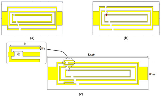
Figure 5.
Proposed structure: (a) without gaps and stubs; (b) with gaps; (c) with gaps and stubs.
4. Numerical Study and Discussion
To reach better performances of the proposed structure, a parametric study was performed, through several simulations, by using Computer System Technology (CST), a leader commercial electromagnetic simulator. The goal of this study is to highlight the effect of the employed gap and stub techniques on the impedance of the proposed design.
4.1. Effect of the Gaps and Stubs on Antenna Performance
The first simulation study concerns the effect of adding gaps and stubs on the real and imaginary parts of the antenna’s impedance. As expected, the impedance of the structure varies, and its real and imaginary parts values become near to that of an industrial chip when introducing gaps and stubs as illustrated in Figure 6. Adding stubs as well as gaps influences more the impedance of the antenna because the imaginary part of the impedance can reach higher positive values and the real one can attain lower positive values, i.e., at f = 916 MHz as an example.
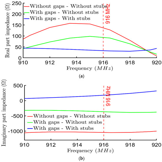
Figure 6.
Proposed structure impedance with different configurations: without stubs without gaps; without stubs with gaps; with stubs with gaps: (a) The real part of the impedance; (b) The imaginary part of the impedance.
These variations in the antenna impedance strongly impact its return loss, and, therefore, its operating frequency and bandwidth, as shown in Figure 7. In fact, the antenna performance is enhanced even more when combining the two techniques into the same structure. Geometrical parameters and positions, of introduced gaps, and stubs can be adjusted to make antenna function at higher or lower frequency bands.
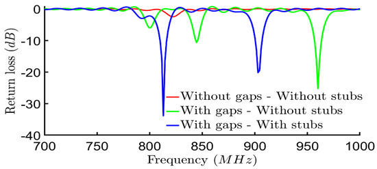
Figure 7.
The return loss of the proposed structure vs. different configuration: without stubs without gaps; without stubs with gaps; with stubs with gaps.
4.2. Effect of the Gaps Dimensions
According to Equation (5), adding a gap to the antenna structure induces a capacitive effect that is relative to the gap lengths as shown in Figure 8. To investigate how the gap length affects the performance of the antenna, a numerical study is performed on the proposed antenna versus different gap length values (lg = 0, 0.5, 1, 1.5, and 2 mm). The change in impedance with respect to the gap lengths is illustrated in Figure 8. In general, creating a gap significantly reduces the impedance (both real and imaginary parts) of the structure. However, the impedance values, when lg varies from 1 mm to lg 2 mm, are nearly similar. These two gap lengths are distanced equally from substrate thickness value, h = 1.5 mm, which suggests that structure’s thickness can have an important influence on the parameter’s configuration [14].
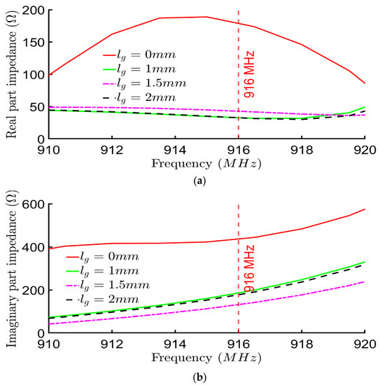
Figure 8.
The proposed structure impedance vs. different gap lengths lg: (a) The real part of the impedance; (b) The imaginary part of the impedance.
Figure 9 shows the effect of the gap length on the return loss of the proposed antenna structure. By changing the gap length, the antenna impedance varies, which influences the return loss. In fact, the resonant frequencies shift (functioning frequencies) upon the gap length in both directions can be retrieved according to Equation (5). When the gap length increases, the functioning frequency shifts to higher values. However, when the gap length surpasses the structure thickness, h = 1.5 mm, the capacitance generated by the gap becomes negative. Hence, the functioning frequency when lg = 2 mm shifts back to a lower value as shown in Figure 9. Furthermore, the effect of the gap length on the operating frequency and defined bandwidth remains limited so that it can further improve the return loss values.
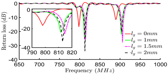
Figure 9.
The return loss of the proposed structure vs. different gap lengths lg without stubs.
4.3. Effect of Introduced Stubs
4.3.1. Effect of Stub Width
The effect of changing the stub width ws on the structure impedance is shown in Figure 10. The change in the real part of the impedance is limited but its imaginary part decreases as the stub width ws increases. These variations in impedance will automatically affect the return loss results as shown in Figure 11 where S11 values, in dB, are plotted in terms of the stub width.
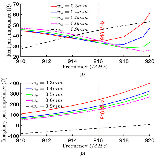
Figure 10.
Proposed structure impedance vs. different stub width ws: (a) Real part variation of the impedance; (b) Imaginary part variation of the impedance.
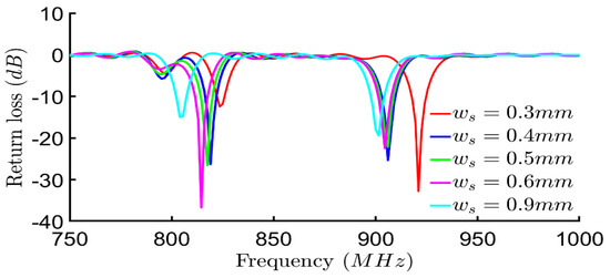
Figure 11.
The return loss of the proposed structure with different stub width.
When ws increases the imaginary part decreases, hence the resonant frequency (corresponds to the lowest value of S11 parameter) shifts toward lower frequencies in both LF and HF regions. We must note also that in HF region, the minimal return loss value increases as ws increases. On the contrary, this effect is reversed in LF region because minimal return loss value goes up as ws decreases except for ws = 0.9 mm.
4.3.2. Effect of Stubs’ Length
The stub length is another parameter that helps control the structure impedance. Figure 12 illustrates how this parameter can affect the structure impedance. It looks difficult to interpret the relationship between impedance real part variations and the stub length ls, however, its interval values go, approximatively, from 20 to 50 Ω at 916 MHz. Concerning the imaginary impedance part, it is clear that it increases significantly as the stub length increases.
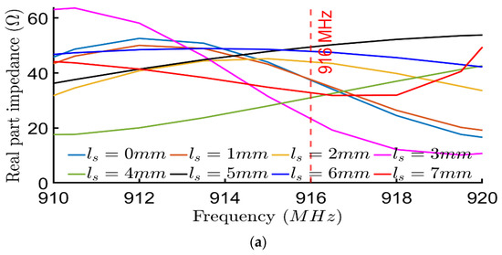
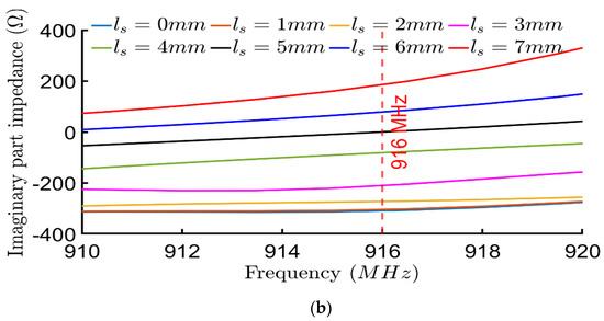
Figure 12.
The proposed structure impedance vs. different stubs’ length ls: (a) The real part of the impedance; (b) The imaginary part of the impedance.
As seen before, return loss will depend on the stub length, ls, as this latter affects the antenna impedance. Figure 13 shows the return loss versus different stubs length values. In fact, resonant frequency shifts toward high values, in both LF and HF regions, as the ls decreases. Furthermore, return loss improves when the value of ls increase.
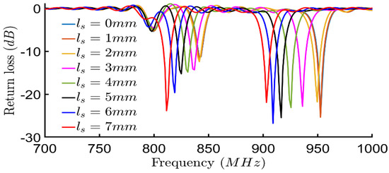
Figure 13.
Return loss parameter of the proposed structure vs. different stub lengths ls.
4.3.3. The Combined Effect of the Stub Length ls and Width ws
Figure 14 plots the minimum values of the return loss with respect to the stub dimensions, ls and ws, in both LF and HF regions. In general, the proposed antenna structure performs better in HF region than in the LF region. In the HF region, the return loss is below −20 dB for multiple combinations of ls and ws and attains −33 dB for ls 5 mm and ws = 0.4 mm. In the LF region, the minimal value of the return loss is obtained when ws = 0.5 mm and ls = 7 mm. Furthermore, the antenna performance in LF and HF regions decreases as the return loss increases, this happens when ls and ws are important.
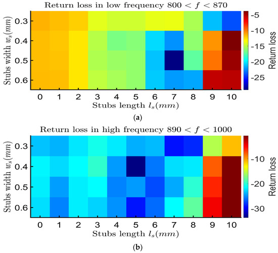
Figure 14.
Return loss vs. ls and ws values. (a) at low frequency 800 < f < 870, (b) at high frequency 890 < f < 1000.
4.4. Optimal Antenna Structure
The previous numerical studies investigated the effect of added gaps and stubs to the antenna structure on its performance. The length of gaps, and the stub dimensions play an important role in satisfying the matching conditions, where the input impedance of the tag antenna (Zantenna = 27 + j187) corresponds closely to the complex conjugate to that of the chip (Zchip = 16 − j194), , at 916 MHz. Moreover, according to Friis’s free-space formula, when the matching conditions are satisfied the maximum readable range is reached. Hence, the length of gaps and stub parameters will strongly affect the proposed RFID antenna read range.
Figure 15 presents the calculated return loss values of the optimal RFID structure when gaps and stubs are set at their optimal dimension’s values: lg = 2 mm, ls = 7 mm, and ws = 0.6 mm, and when it is fed by an MPING M70 chip. This structure achieves a lower return loss value of −22.3 dB in the HF region at 916 MHz which offers a maximum calculated read range value up to 25 m.
Figure 15.
Return loss when the RFID antenna is fed by an MPING M70 chip.
The main purpose of previous numerical studies is to investigate the effect of creating gaps and adding stubs on the antenna performance, especially its read range parameter which can qualify it for localization applications. The results of the simulation study illustrated clearly how antenna performances can be enhanced by combining the two approaches and tuning the size of each element.
5. Experimental Results
Section 5 aims to validate the simulation study and verify the advantages of adding gaps and stubs to the antenna structure in real applications. For this kind, a prototype of the simulated RFID tag antenna has been fabricated and tested, as shown in Figure 16, using Taconic RF-60 substrate of permittivity 6.12 and a thickness of 1.6 mm. The fabricated tag has a size of 95 × 25 mm2 and includes gaps of length lg = 2 mm, stubs of width ws = 0.6 mm, and length ls = 5 mm.
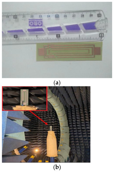
Figure 16.
Experimental results. (a) Fabricated Antenna. (b) Proposed UHF antenna tested inside the anechoic chamber.
Figure 17 presents the measured and simulated results of the reflection coefficient. The two curves are much closer to each other especially around the two resonant frequencies with a slight shift of the measurements toward higher frequency band. Experimental results show that the proposed RFID tag is a dual-band antenna operating at UHF band around 837 MHz (LF region) and around 927 MHz (HF region). In the LF region, the antenna has a measured return loss near to −15 dB at 840 MHz with a 6 MHz bandwidth (838–844 MHz). In the HF region, the measured return loss is even better as it reaches −17 dB at 927 MHz, with a 10 MHz bandwidth (925–935 MHz).
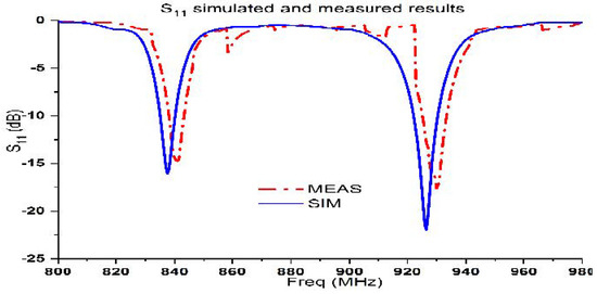
Figure 17.
Reflection coefficient (S11): simulations versus measurements.
In addition, radiation pattern simulations and measurements have been performed. The results presented in Figure 18 note that our proposed antenna is an omnidirectional radiator, in both frequency bands, with a large half-power beamwidth (HPBW) which is recommended for such applications. The measurement and calculated quantities are in very good agreement, which validates our numerical studies and illustrates the performance of CST as a leader electromagnetic simulator.
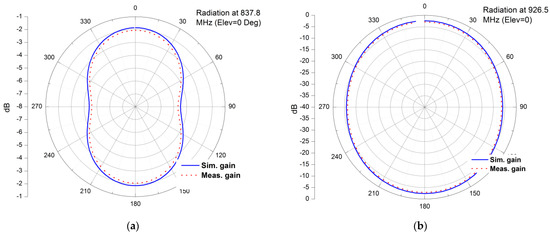
Figure 18.
Radiation of proposed RFID antenna. (a) At 837 MHz. (b) At 927 MHz.
Simulations and experimental results indicate that proposed antenna performances are very promising since they have an important long read-range of 25 m, by using Mping M730 chip with −24 dB sensitivity [16], and an omnidirectional radiation pattern at both frequency bands. In comparison with other antennas reported in the literature, as shown in Table 1, our proposed RFID tag looks to be a promising candidate for localization applications since it can communicate over a large distance at 916 MHz, when it is fed by an appropriate industrial chip, in all horizontal directions, and can behave as a dual-band antenna when the feeder is a 50 Ω port while most other antennas function in a particular band.

Table 1.
The performances of the antennas proposed in the literature vs. the performance of the proposed antenna.
6. Conclusions
This paper introduces a new antenna structure design for RFID tags dedicated to localization applications. The proposed structure uses two techniques, thereby tuning its input impedance and achieving a good impedance matching level when it is connected to a specific chip. The first technique uses gaps to create a capacitive effect that depends on the substrate permittivity and thickness, and gap length. The second technique consists of introducing stubs into the proposed design to adjust its impedance thereby matching it to the corresponding chip output impedance. The effect of the two techniques on antenna performances is illustrated through several numerical studies with various scenarios. According to the obtained results, the proposed optimal antenna structure can radiate in an omnidirectional manner and can operate in dual frequency bands, 837 and 927 MHz, in the case of a 50 Ω RF power source with measured return loss values, respectively, −15 dB and −17 dB. When the same antenna is excited by an industrial chip, of −24 dB power sensitivity and has an output impedance of 16 − j194 (Ω), it accepts power around 916 MHz with a return loss value near to −22.3 dB and can be read from a long distance up to 25 m. Antenna performances have been validated by testing a fabricated prototype where simulated and measured results were in good agreement.
Author Contributions
Conceptualization, R.J., M.A., and A.H., S.A.; methodology, R.J., A.H., and S.A.; software, F.E.M., and S.A.; validation, M.A., N.O.P., C.H.S., R.A.-A., and S.A.; formal analysis, N.O.P., C.H.S., R.A.-A., A.H., and F.E.M.; investigation, R.J., H.O., A.H., and S.A.; resources, R.J., M.A., and S.A.; data curation, A.H., H.O., and R.A.-A. Writing—original draft preparation, R.J., and M.A.; writing—review and editing, R.J., C.H.S., and S.A.; visualization, M.A., S.A., N.O.P., C.H.S., and R.A.-A.; supervision, R.J., and H.O.; project administration, M.A., H.O., and A.H., funding, N.O.P., C.H.S., and R.A.-A. All authors have read and agreed to the published version of the manuscript.
Funding
This paper is partially funded by British Council “2019 UK-China-BRI Countries Partnership Initiative” program, with project titled “Adapting to Industry 4.0 oriented International Education and Research Collaboration”.
Data Availability Statement
The data are available with the author upon request.
Acknowledgments
The authors wish to express their thanks to the support provided by British Council “2019 UK-China-BRI Countries Partnership Initiative” programme with project titled “Adapting to Industry 4.0 oriented International Education and Research Collaboration”.
Conflicts of Interest
The authors declare no conflict of interest.
References
- Stockman, H. Communication by Means of Reflected Power. Proc. IRE 1948, 36, 1196–1204. [Google Scholar] [CrossRef]
- Duroc, Y.; Tedjini, S. RFID: A key technology for Humanity. C. R. Phys. 2018, 19, 64–71. [Google Scholar] [CrossRef]
- Byondi, F.K.; Chung, Y. Longest-range UHF RFID sensor tag antenna for iot applied for metal and non-metal objects. Electronics 2019, 19, 5460. [Google Scholar] [CrossRef] [PubMed]
- Chung, Y.; Berhe, T.H. Radiation Beam Pattern Control of UHF RFID Tag Antenna Design for Automotive License Plates. Electronics 2021, 10, 2439. [Google Scholar] [CrossRef]
- Rao, K.V. Overview of back scattered radio frequency identification system (RFID). In Proceedings of the Asia-Pacific Microwave Conference Proceedings, APMC, Singapore, 30 November–3 December 1999; Volume 3, pp. 746–749. [Google Scholar]
- Nath, B.; Reynolds, F.; Want, R. RFID technology and applications. IEEE Pervasive Comput. 2006, 5, 22–24. [Google Scholar] [CrossRef]
- Want, R. An introduction to RFID technology. IEEE Pervasive Comput. 2006, 5, 25–33. [Google Scholar] [CrossRef]
- Tedjini, S.; Vuong, T.P.; Beroulle, V. Antennas for RFID tags. ACM Int. Conf. Proc. Ser. 2005, 121, 19–22. [Google Scholar]
- El Hamraoui, A.; Abdelmounim, E.H.; Zbitou, J.; Elabdellaoui, L.; Bennis, H.; Latrach, M. A new compact CPW-fed dual-band uniplanar antenna for RFID applications. Telkomnika 2018, 16, 102–109. [Google Scholar] [CrossRef]
- Domdouzis, K.; Kumar, B.; Anumba, C. Radio-Frequency Identification (RFID) applications: A brief introduction. Adv. Eng. Inform. 2007, 21, 350–355. [Google Scholar] [CrossRef]
- Ferchichi, A.; Azizi, M.K.; Ali, G. Analysis of a Square Parasitic Antenna by Using Lumped Elements. Int. J. Electron. Telecommun. 2012, 58, 279–283. [Google Scholar] [CrossRef][Green Version]
- Shafiei, M.M.; Moghavvemi, M.; Wan Mahadi, W.N.L. The Parametric Study and Fine-Tuning of Bow-Tie Slot Antenna with Loaded Stub. PLoS ONE 2017, 12, e0169033. [Google Scholar] [CrossRef] [PubMed]
- Singh, S.; Verma, S. SAR reduction and gain enhancement of compact wideband stub loaded monopole antenna backed with electromagnetic band gap array. Int. J. RF Microw. Comput.-Aided Eng. 2021, 31, e22813. [Google Scholar] [CrossRef]
- Srikant, S.S.; Mahapatra, R.P. Read Range of UHF Passive RFID. Int. J. Comput. Theory Eng. 2010, 2, 323–325. [Google Scholar] [CrossRef]
- Bahl, I. Lumped Elements for RF and Microwave Circuits; Artech House: London, UK, 2013; Volume 53, pp. 1689–1699. [Google Scholar]
- Datasheet, T.A.G.C. IMPINJ M700 SERIES 2020. Available online: https://www.impinj.com/ (accessed on 10 February 2022).
- Bansal, A.; Sharma, S.; Khanna, R. Compact meandered RFID tag antenna with high read range for UHF band applications. Int. J. RF Microw. Comput.-Aided Eng. 2019, 29, e21695. [Google Scholar] [CrossRef]
- Ma, Z.L.; Jiang, L.J.; Xi, J.; Ye, T.T. A Single-Layer Compact HF-UHF Dual-Band RFID Tag Antenna. IEEE Antennas Wirel. Propag. Lett. 2012, 11, 1257–1260. [Google Scholar]
- He, S.; Zhang, Y.; Li, L.; Lu, Y.; Zhang, Y.; Liu, H. High performance UHF RFID tag antennas on liquid-filled bottles. Prog. Electromagnet Res. 2019, 165, 83–92. [Google Scholar] [CrossRef]
- Braaten, B.D.; Reich, M.; Glower, J. A compact meander-line UHF RFID tag antenna loaded with elements found in right/lefthanded coplanar waveguide structures. IEEE Antennas Wirel. Propag. Lett. 2009, 8, 1158–1161. [Google Scholar] [CrossRef]
- Nguyen, M.T.; Lin, Y.F.; Chen, C.H.; Chang, C.H.; Chen, H.M. Shorted patch antenna with multi slots for a UHF RFID tag attached to a metallic object. IEEE Access 2021, 9, 111277–111292. [Google Scholar] [CrossRef]
- Chung, Y.; Berhe, T.H. Long-Range UHF RFID Tag for Automotive License Plate. Sensors 2021, 21, 2521. [Google Scholar] [CrossRef] [PubMed]
- Lu, Y.; Marty, F.; Galayko, D.; Laheurte, J.M.; Basset, P. A MEMS EVEH-Assisted Long-Range RFID Tag System for Applications with Low-Frequency Vibrations. Proceedings 2017, 1, 582. [Google Scholar]
Publisher’s Note: MDPI stays neutral with regard to jurisdictional claims in published maps and institutional affiliations. |
© 2022 by the authors. Licensee MDPI, Basel, Switzerland. This article is an open access article distributed under the terms and conditions of the Creative Commons Attribution (CC BY) license (https://creativecommons.org/licenses/by/4.0/).