Article

A General Parameter Optimization Method for a Capacitive Power Transfer System with an Asymmetrical Structure

1
State Key Laboratory of Automotive Simulation and Control, Jilin University, Changchun 130025, China
2
Department of Electrical Engineering, Kunming University of Science and Technology, Kunming 650500, China
3
CSG Electric Power Research Institute of Yunnan Power Grid Corporation, Kunming 650106, China
*
Author to whom correspondence should be addressed.
Electronics 2022, 11(6), 922; https://doi.org/10.3390/electronics11060922
Submission received: 18 February 2022 / Revised: 13 March 2022 / Accepted: 14 March 2022 / Published: 16 March 2022

Abstract

:
Capacitive power transfer (CPT) is an attractive wireless power transfer (WPT) technology and it has been widely studied in many applications. Symmetrical structures and high-order compensation networks are always produced as optimization results and common configurations for high-efficiency CPT systems. However, in space-limited scenarios, an asymmetric structure tends to be a better choice. The related large number of high-order asymmetric system parameters is a key problem in parameter design. In this study, a general parameter design method that is based on reactive power optimization is proposed for an electric field resonance-based CPT system with an asymmetric six-plate coupler. The reactive power in the compensation network was analyzed and optimized under the constraint of transferred power. With equal reactive power, the optimization complexity was significantly reduced and the optimized system parameters were provided. To validate the effectiveness of the proposed method, a 1 MHz, 3.2 kW asymmetric CPT protype with 100 mm gap distance was implemented. The results indicate that, with the optimized parameters, high system efficiency can be achieved when the system’s volume is reduced. At the rated power, about 95% DC–DC overall efficiency was achieved through a 6-pF coupling capacitor.

1. Introduction

Wireless power transfer (WPT) technology that offers a way to transfer electric power through air or other another nonconductive medium has more advantages than traditional conductive charging technology [1,2,3]. In recent years, WPT technologies have been widely studied and many commercialized products have been released in low-power and high-power applications [4,5,6,7], such as consumer electronics [8,9,10,11], electrical machines [12,13,14], biomedical devices [15,16,17,18,19], and transportation systems [20,21,22,23,24,25]. Among the WPT technologies, inductive power transfer (IPT) and capacitive power transfer (CPT) are the two main types in which a magnetic field or an electric field is utilized for power transmission, respectively.
Inductive wireless power transfer is one of the most promising WPT technologies and extensive studies have been implemented on the IPT system. In the IPT system, the magnetic coupler is a key component that always consists of transmission coils with a symmetric or asymmetric structure [26]. Since the magnetic couplers are always loosely coupled [27], heavy ferrite cores are needed in order to redistribute the magnetic field in the coupler and enhance the magnetic coupling of the transmission coils. Besides this, shielding plates are required to prevent the magnetic field from leaking into the surrounding environment. To improve the transferred power and efficiency, compensation circuits are needed in order to achieve circuit resonance. The basic compensation circuit topology is just one resonant capacitor that is connected in series or parallel with each of the transmission coils [28,29,30]. The high-order compensation circuit’s topology consists of a complex circuit structure, such as inductance–capacitance–capacitance (LCC) [31,32], inductance–capacitance–inductance (LCL) [33], series–series–parallel (S-SP) [34,35], or series–parallel–series (SP-S) [36]. With more freedom within their parameter design than in those of a basic compensation circuit, high-order compensation circuits can achieve zero-voltage switching (ZVS), zero phase angle (ZPA), and a constant current/voltage (CC/CV) output at the same time with appropriate parameter design [37,38]. Within compensation circuits, the transferred power of IPT systems can be up to ten kilowatts (kW) under a transmission distance of hundreds of mm and the transmission efficiency can be up to 90–96% [31,39]. However, due to the eddy current effect, the magnetic field in the coupler can cause a huge temperature rise in the surrounding metal objects, which threats the operation of the system [40]. In contrast, the electric field in the capacitive coupler, which is used for power transmission in CPT systems, does not cause a significant temperature rise in metal objects [41]. Besides this, the capacitive coupler always consists of several metal plates. Compared with the expensive and heavy ferrite cores that are found in IPT systems, the cost and weight of the CPT system can be reduced. Therefore, the CPT system is becoming an attractive alternative for the IPT system and an increasing amount of research is focused on CPT technologies, recently [5].
In the literature regarding CPT systems, most of the research focuses on the design of the capacitive coupler and compensation circuit [5]. The capacitive coupler in the CPT system is always made up of several metal plates with a rectangular or circular shape. The coupling structure can be configured in a rotating [42], horizontal [25,43], vertical [44], or interleaved style [45]. Generally, there are at least four plates in the capacitive coupler, two of which are set as transmitting plates and the other two plates are set as receiving plates. The mutual capacitances are generated between the transmitting plates and receiving plates. In order to improve the transferred power and efficiency, the compensation circuits are needed to make the circuit resonant, which allows it to achieve zero phase angle (ZPA) on the grid side [40]. Just like the IPT system, the basic compensation circuit of the CPT system is just one inductor connected in series or parallel with the capacitive coupler at the transmitting side and receiving side [46,47], respectively. However, in long-distance applications, the mutual capacitance of the coupler is very small (usually in the range of several to tens of picofarads), which makes the compensation inductors very large (usually in the range of several millihenry). To further improve the transferred power and reduce the value of the compensation inductors, a high frequency and high-order compensation circuit is needed [40]. Nowadays, the operating frequency of a CPT system is usually in the range of several or tens of megahertz (MHz). High-order compensation circuits, such as LCL [44,48], electric field resonance (EFR) [49,50], capacitance-inductance-inductance-capacitance (CLLC) [51], multistage LC [52,53], and inductance-capacitance-inductance-capacitance (LCLC) [25,40] compensation circuits, provide large voltage gains and improve the capability of power transmission. With these compensation circuits, the transferred power of the CPT system can be up to several kW and the transmission distance can be up to hundreds of mm; the system’s performance is significantly improved. In [25,40], a double-sided LCLC compensation circuit was used for a horizontal four-plate coupler, about 1.5 kW of power was transferred through a 150 mm transmission distance with a DC–DC overall efficiency of 93.5% [40]. However, the coupling plate voltage can be up to several kilovolts, which may be excessive of the safety limit, causing electromagnetic radiation (EMR) problems and serious security incidents. As a solution, shielding structures were added to the traditional four-plate coupler and a six-plate coupler was proposed in [48,49]. With the shielding plates covering over the capacitive coupler, the electric field emission can be significantly reduced. Besides this, the parasitic capacitance of the shielding plates can also be used as the resonant capacitance, which can eliminate the external capacitance of the compensation circuit, such as makes the LCLC compensation circuit into a LCL compensation circuit [44]. In [49], a six-plate coupler-based EFR compensation circuit was proposed and about 91.1% DC–DC overall efficiency was achieved with a transferred power of 700 W. However, high-order compensation circuits increase the total number of circuit parameters. A large number of circuit parameters make it difficult to design and optimize the system’s parameters. To optimize the circuit’s parameters and improve the system’s efficiency, Lagrange multipliers and two-stage optimization methods were proposed in [50,53,54,55,56]. In [53,54,55,56], the multistage LC matching networks were analyzed by using the method of Lagrange multipliers and the number of matching network stages and the distribution of the gains and compensation among the stages were optimized in order to achieve high-efficiency matching networks. Reference [50] proposes a two-stage parameter design method for an EFR-based CPT system, which can optimize the system parameters through optimizing the reactive power in the coupling capacitor CS and the whole system. With the proposed two-stage method, when 3 kW of power is transferred over a distance that is under 100 mm, the system efficiency can be up to 95.7%. According to the optimization results in [50,53,54,55,56], the optimized CPT systems tend to have symmetric circuit parameters when the compensation circuits on the primary side and secondary side are the same. The coupling structures of the capacitive coupler are also symmetric. However, in many practical applications, especially for mobile devices [57], unmanned aerial vehicles [58,59], and electric vehicles (EVs) wireless charging applications [60,61], the available installation space on the receiving side is always smaller than that which is available on the transmitting side, which limits the volume of the receiver. In these scenarios, the receiver needs to be compact and flat. An asymmetric coupler structure is an effective configuration for the WPT systems that are used in these applications [59]. The asymmetric coupler structure leads to asymmetric system parameters. The optimization results from symmetric cases are not suitable for a system with asymmetric parameters and the use of systematic parameter optimization methods for asymmetric CPT systems is rarely mentioned in previous studies.
In this present study, an EFR-based six-plate capacitive coupler with an asymmetric structure was used in order to make an asymmetric CPT system for EV wireless charging applications. A general parameter optimization method that is based on reactive power optimization is proposed for this asymmetric CPT system. A capacitive coupler with different geometry was analyzed and modeled. According to the circuit model, the appropriate voltage and current were obtained in order to derive the system’s reactive power. Under the constraint of transferred power, the reactive power was optimized based on the independence of the circuit parameters. By using equal reactive power, the general circuit conditions under which the circuit parameters should be satisfied were derived. With these circuit conditions, the optimization complexity was reduced and the optimized asymmetric system parameters were given.
The following is the organization of this paper. Section 2 introduces the asymmetric coupling structure and the modeling of the asymmetric CPT system. Based on this circuit model, the system’s reactive power and its effect on the system’s efficiency are derived. Section 3 analyzes the independence of the circuit parameters and proposes a general parameter optimization method. Section 4 introduces the implementation of this method. The effectiveness of the proposed method is verified in Section 5. Section 6 provides the conclusions.

2. Modelling of the CPT System

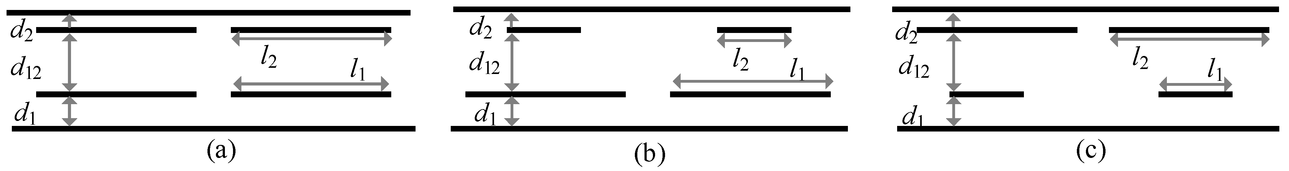
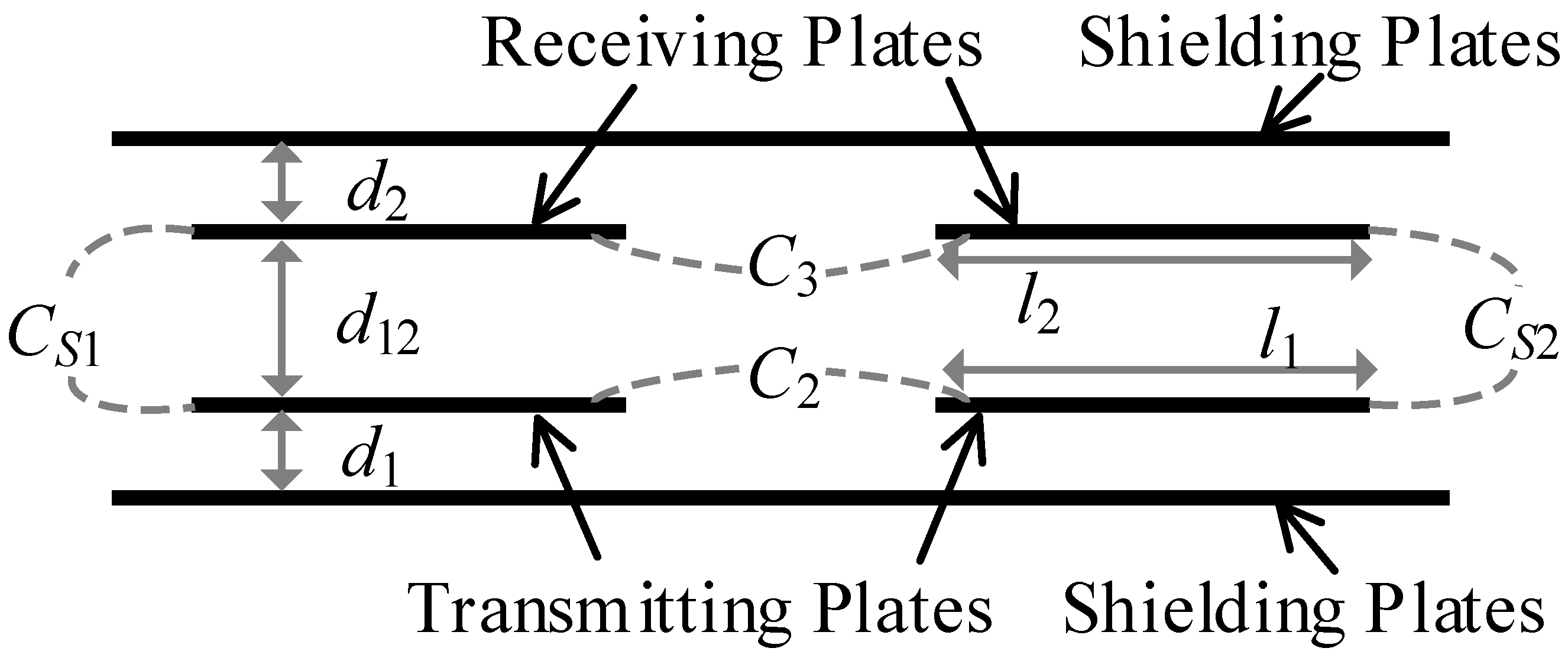
2.1. Asymmetrical Capacitive Coupler Model

A capacitive coupler that consists of six rectangular metal plates was used in this experiment. The typical structure is shown in Figure 1. l1 and l2 are the plate lengths, d1, d2, and d12 are the airgap distances. There were 15 coupling capacitors in the six-plate coupler and the performance of this structure can be characterized by four primary capacitors, CS1, CS2, C2, and C3. CS1 and CS2 represent the equivalent mutual capacitors between the transmitting plates and receiving plates; C2 and C3 represent the equivalent self-capacitors between the transmitting plates or between the receiving plates. The equivalent circuit model with four coupling capacitors is shown in Figure 2a [48]. Due to the fact that the capacitors CS1 and CS2 are connected in series, the coupling capacitor CS can be further simplified, where
C S = C S 1 C S 2 C S 1 + C S 2
As described in [50], a symmetric CPT system with an identical transmitter and receiver is verified to be an efficient configuration. However, the shielding distances d1 and d2 tend to have large values (usually in the range of 50 mm to 100 mm) in order to achieve high system efficiency. For space-limited scenarios, such as EV wireless charging applications, the limited space in the receiving side determines that the shielding distance d2 cannot be very large. Therefore, an asymmetric coupler with different distances d1 and d2 (where d1 > d2) is more practical in EV wireless charging applications. According to the different plate lengths l1 and l2, the asymmetric structure can be divided into three categories: l1 = l2, l1 > l2, and l1 < l2, as shown in Figure 3.
In the capacitive coupler, the coupling capacitors C2, C3, and CS are determined by the airgap distances d1, d2, and d12 and plate lengths l1 and l2. An asymmetric coupler structure always results in asymmetric circuit parameters. In Figure 3a and c, l1 is not greater than l2 and d1 is greater than d2, as a result the capacitor value of C2 is less than that of C3. In Figure 3b, the relationship between C2 and C3 is determined by the asymmetric distance and plate length and the equivalent C2 and C3 can be obtained by appropriate configuration. When the plate lengths l1 and l2 are not equal, as shown in Figure 3b,c, a small horizontal misalignment has little effect on the coupling capacitance. In the cases in which l1l2, as shown in Figure 3a,b, the leaked electric field that results from the small misalignment conditions are mostly exposed to the receiving side. As a comparison, the leaked electric field that results from small misalignment conditions for the asymmetric coupler that is shown in Figure 3c are mostly exposed to the transmitting side. Considering this, the asymmetric structure that is shown in Figure 3c was selected in order to form the asymmetric CPT system in this study.

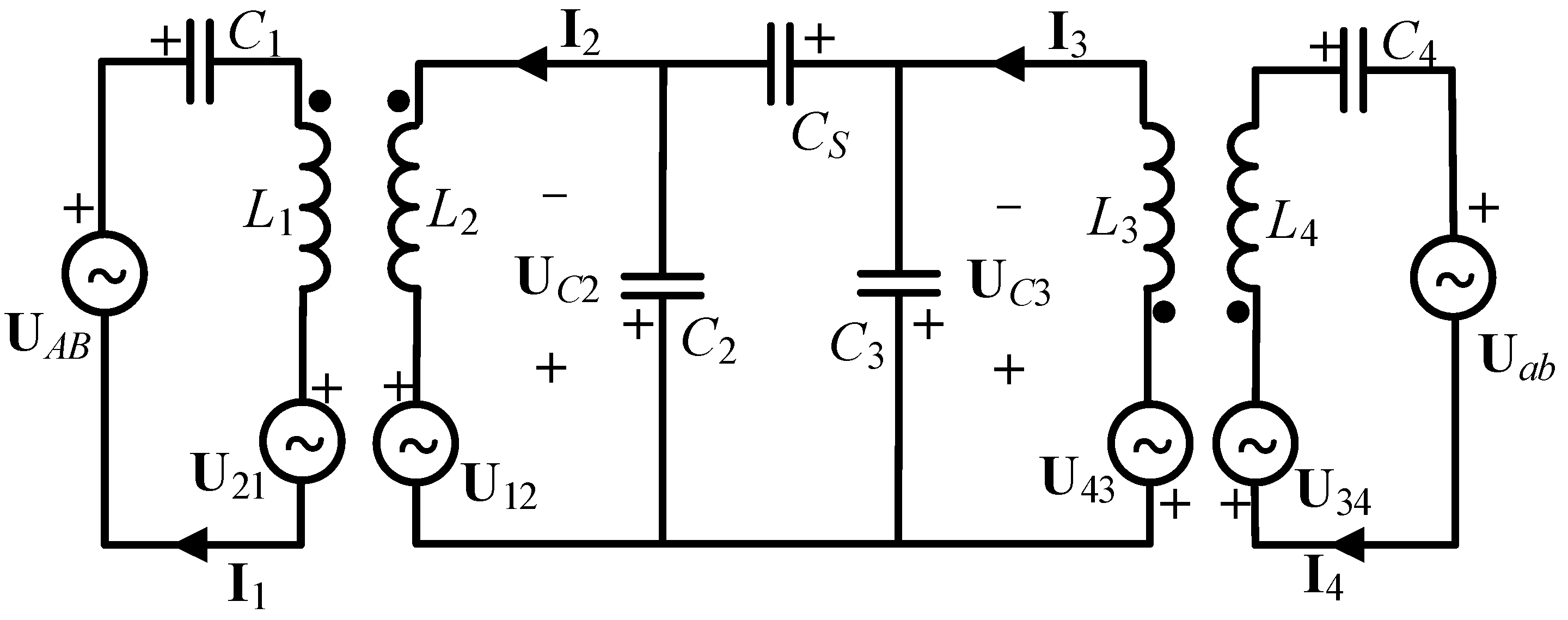
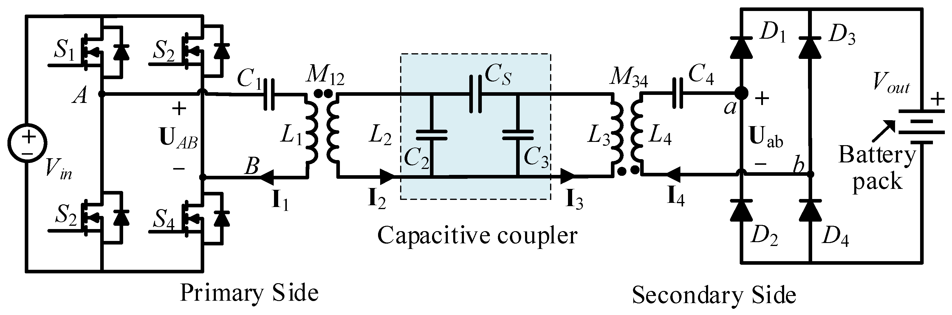
2.2. CPT System Model

In this study, an EFR compensation network was used. With the asymmetric capacitive coupler that is shown in Figure 3c, the equivalent circuit model of the asymmetric CPT system is shown in Figure 4, where C3 is greater than C2. The EFR compensation circuit was formed by L1, C1, L2, C2, L3, C3, L4, and C4. M12 and M34 represent the mutual inductances between L1 and L2 and between L3 and L4, respectively. CS represents the mutual capacitance in the capacitive coupler. Vin and Vout are the input and output direct current (DC) voltage sources, respectively. The capacitors C2, C3, and CS achieve EFR in the compensation circuit and the EFR is resonant with the inductors L2 and L3 at an angular frequency of ω0. Besides this, C1 and C4 are resonant with L1 and L4 at an angular frequency of ω0, respectively.
As shown in Figure 5, the equivalent circuit model of an EFR-based CPT system can be obtained according to the method of fundamental harmonics approximation. The internal resistances of all of the circuit components are ignored. U21, U12, U43, and U34 represent the induced voltage sources that are generated in the coupling inductors L1, L2, L3, and L4. UAB and Uab represent the input and output AC voltages, respectively, where
{ U A B = V i n 2 2 / π U a b = V o u t 2 2 / π
By using UAB as the reference, the voltage and current phasors can then be obtained based on the superposition theorem as follows [50]:
{ U A B = U A B 0 ° = U A B U a b = U a b 90 ° = j U a b U C 2 = U A B M 34 ( C 3 + C S ) + U a b M 12 C S ω 0 2 M 12 M 34 ( C 3 C S + C 2 C S + C 2 C 3 ) U C 3 = U A B M 34 C S + U a b M 12 ( C 2 + C S ) ω 0 2 M 12 M 34 ( C 3 C S + C 2 C S + C 2 C 3 ) I 1 = U a b C S j ω 0 3 M 12 M 34 ( C 3 C S + C 2 C S + C 2 C 3 ) I 2 = j U A B ω 0 M 12 I 3 = j U a b ω 0 M 34 I 4 = j U A B C S ω 0 3 M 12 M 34 ( C 3 C S + C 2 C S + C 2 C 3 )
We can see from Equation (3) that the current and voltage phasors on the input side are in phase, which means zero phase angle is achieved on the input side. Since all of the internal resistances are not considered, the output power is equal to the input power, which can be described as
P = U A B I 1 = U a b I 4 = U A B U a b C S ω 0 3 M 12 M 34 ( C 2 C 3 + C 2 C S + C 3 C S )
The mutual inductances M12 and M34 that are featured in Equation (4) can be described as
{ M 12 = K 12 1 ω 0 2 C 1 C 3 + C S ω 0 2 ( C 2 C 3 + C 3 C S + C 3 C S ) M 34 = K 34 1 ω 0 2 C 4 C 2 + C S ω 0 2 ( C 2 C 3 + C 3 C S + C 3 C S )
where K12 and K34 are the coupling coefficients. By substituting Equation (5) into Equation (4), the transferred power can be further described as
P = ω 0 C S U A B U a b C 1 C 4 K 12 K 34 ( C 3 + C S ) ( C 2 + C S )

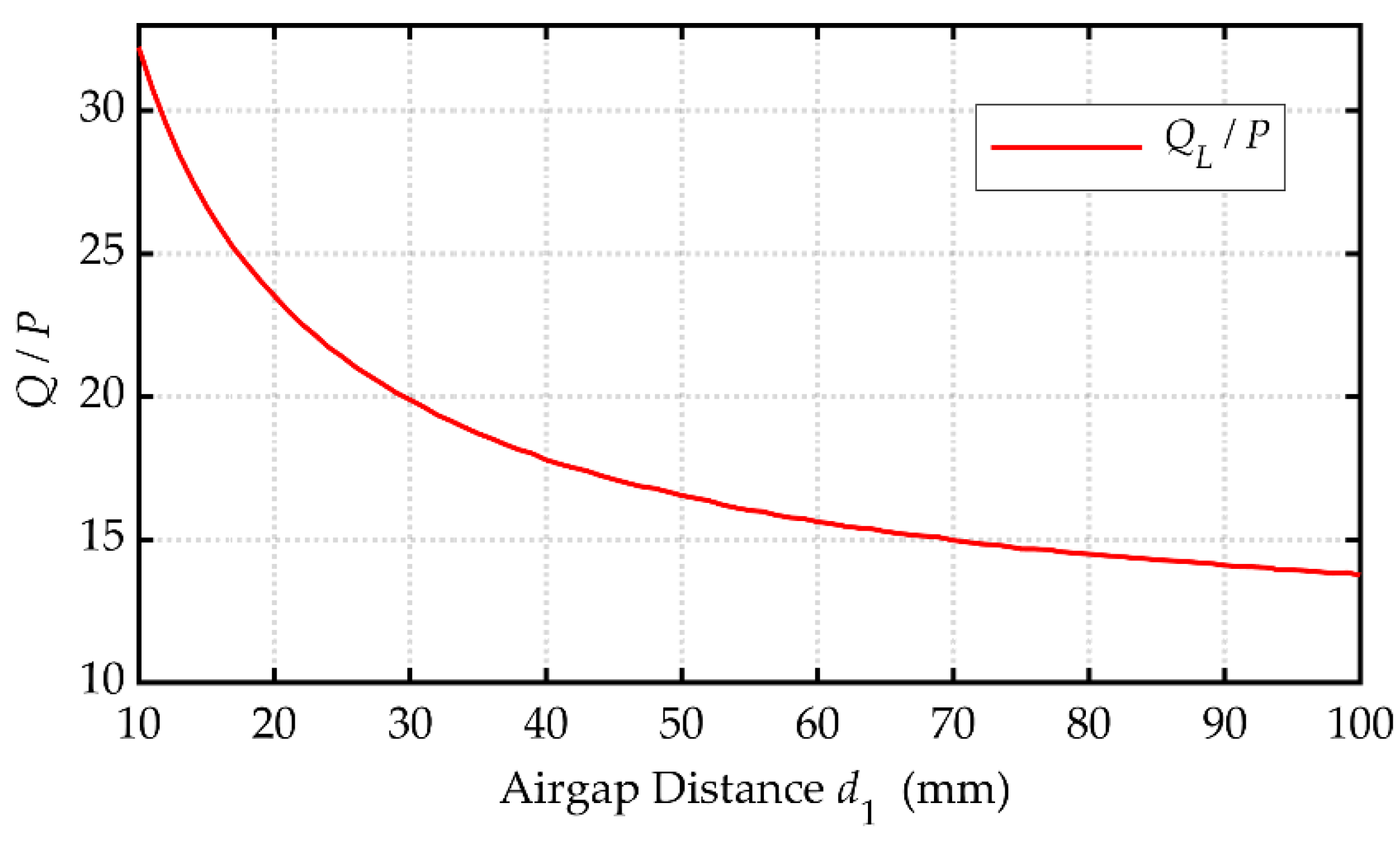
2.3. Reactive Power on a Compensation Network

According to Equations (3) and (5), the capacitive reactive power in the system that is shown in Figure 5 can be obtained as follows:
{ Q C 1 = ω 0 U a b 2 C 4 C S 2 K 12 2 K 34 2 ( C 3 + C S ) ( C 2 + C S ) Q C 2 = ω 0 K 34 2 U A B 2 C 1 C 2 ( C 3 + C S ) ( C 2 + C S ) 2 + ω 0 K 12 2 U a b 2 C 2 C 4 ( C 3 + C S ) C S 2 K 12 2 K 34 2 ( C 2 C 3 + C 3 C S + C 3 C S ) ( C 3 + C S ) ( C 2 + C S ) Q C 3 = ω 0 K 12 2 U a b 2 C 4 ( C 3 + C S ) ( C 2 + C S ) 2 C 3 + ω 0 K 34 2 U A B 2 C 1 ( C 2 + C S ) C S 2 C 3 K 12 2 K 34 2 ( C 2 C 3 + C 3 C S + C 3 C S ) ( C 3 + C S ) ( C 2 + C S ) Q C 4 = ω 0 U A B 2 C 1 C S 2 K 12 2 K 34 2 ( C 3 + C S ) ( C 2 + C S ) Q C S = ω 0 K 34 2 U A B 2 C 1 ( C 2 + C S ) C S C 3 2 + ω 0 K 12 2 U a b 2 C 4 ( C 3 + C S ) C S C 2 2 K 12 2 K 34 2 ( C 2 C 3 + C 3 C S + C 3 C S ) ( C 3 + C S ) ( C 2 + C S )
Here, QC is used to represent the total capacitive reactive power, where
Q C = Q C S + Q C 1 + Q C 2 + Q C 3 + Q C 4 = ω 0 C 1 U A B 2 ( C S 2 K 12 2 K 34 2 ( C 3 + C S ) ( C 2 + C S ) + 1 K 12 2 ) + ω 0 C 4 U a b 2 ( C S 2 K 12 2 K 34 2 ( C 3 + C S ) ( C 2 + C S ) + 1 K 34 2 )
According to Equations (3) and (5), the reactive power on inductors l1, l2, l3, and l4 can be calculated as follows:
{ Q L 1 = ω 0 C 4 U a b 2 C S 2 K 12 2 K 34 2 ( C 3 + C S ) ( C 2 + C S ) Q L 2 = ω 0 C 1 U A B 2 K 12 2 Q L 3 = ω 0 C 4 U a b 2 K 34 2 Q L 4 = ω 0 C 1 U A B 2 C S 2 K 12 2 K 34 2 ( C 3 + C S ) ( C 2 + C S )
The total inductive reactive power QL can be described as
Q L = Q L 1 + Q L 2 + Q L 3 + Q L 4 = ω 0 C 1 U A B 2 ( C S 2 K 12 2 K 34 2 ( C 3 + C S ) ( C 2 + C S ) + 1 K 12 2 ) + ω 0 C 4 U a b 2 ( C S 2 K 12 2 K 34 2 ( C 3 + C S ) ( C 2 + C S ) + 1 K 34 2 )
Since the CPT system is in a resonant state, the total capacitive reactive power and total inductive reactive power are equal. We can see from Equations (7)–(10) that the reactive power is excited by the voltage sources UAB and Uab. Since the expressions of the reactive power are complex, the optimization of the reactive power is very difficult.

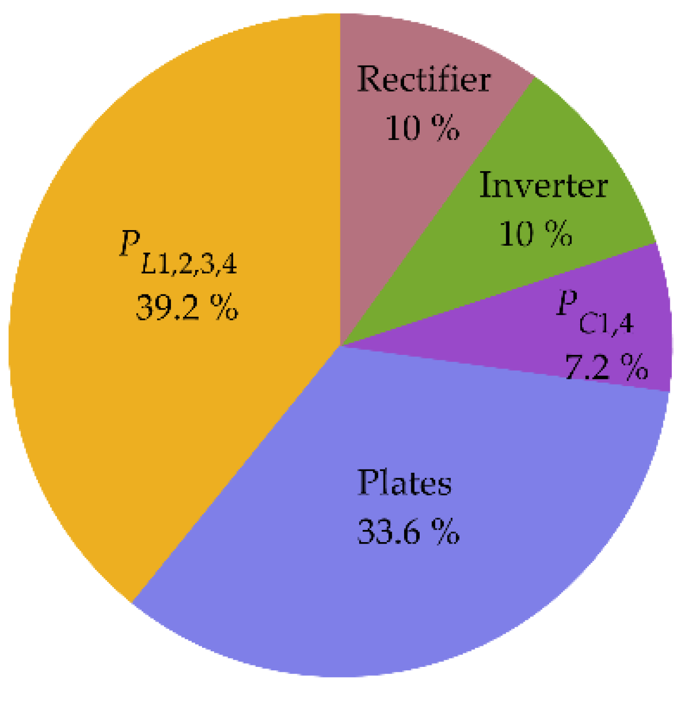
2.4. Analysis of System Efficiency

The efficiency of the CPT system is determined by the transferred power and power losses in the circuit components. Increasing the transferred power while decreasing the losses can improve the transmission efficiency. Typically, the power losses are divided into four main parts: rectifier loss Ploss,rec, inverter loss Ploss,inv, capacitor loss Ploss,C, and inductor loss Ploss,L. Considering these losses, the system’s efficiency η can be expressed as
η = P P + P l o s s , r e c + P l o s s , i n v + P l o s s , C + P l o s s , L
where
{ P l o s s , C = P l o s s , C i P l o s s , L = P l o s s , L j       ( i = S , 1 , 2 , 3 , 4 ; j = 1 , 2 , 3 , 4 )
In Equation (11), the rectifier loss and inverter loss include the switching losses and conduction losses, which are determined by the switching devices and switching states; the losses in the inductors and capacitors are mainly determined by the reactive power that is in the passive components and the quality factors of the components. Therefore, the applications of low conduction-resistance power devices and high quality factor passive components and the realization of a ZVS state are usually efficient methods for the CPT system [40,56]. When the switching devices and transferred power are determined, we assume that the rectifier loss and inverter loss are constants. In this case, the system efficiency can be improved by reducing the losses in the passive components.
Here, the reactive power of the passive components can be represented as QCi and QLj; the quality factors can be represented as Q C i * and Q L j * . The power losses in the passive components can be further described as
{ P l o s s , C i = Q C i Q C i * ,       P l o s s , L j = Q L j Q L j *      P l o s s , C = Q C i Q C i * ,    P l o s s , L = Q L j Q L j * ,       ( i = S , 1 , 2 , 3 , 4 ; j = 1 , 2 , 3 , 4 )
The system efficiency can be obtained from Equations (11)–(13) as
η = 1 1 + Q C i Q C i * P + Q L j Q L j * P + P l o s s , r e c + P l o s s , i n v P      ( i = S , 1 , 2 , 3 , 4 ; j = 1 , 2 , 3 , 4 ) .
In this study, the inductors were wound with Litz wire and the capacitors usually had low dissipation factors. To simplify the analysis, we assumed that all of the capacitors (inductors) had the same quality factors, which can be represented as Q C * ( Q L * ). Given these facts, Equation (14) can be changed to
η = 1 1 + 1 2 ( 1 Q C * + 1 Q L * ) ( Q C P + Q L P ) + P l o s s , r e c + P l o s s , i n v P
where QC and QL represent the total capacitive or inductive reactive power in the CPT system. When the transferred power is determined, the efficiency in Equation (15) can be improved by decreasing the reactive power or increasing the quality factors. When the quality factors are determined, the transmission efficiency is mainly dependent on the reactive power. Therefore, the reactive power in the CPT system should be optimized for efficiency improvement. The cases in which the passive components have different quality factors are described in Appendix A.

3. General Optimization Method

As described above, under the constraint of transferred power, the reactive power should be optimized in order to improve the system’s efficiency. In this case, we set the ratio of reactive power to transferred power as the optimization objective. Based on the properties of a linear CPT system, a general optimization method was proposed in order to reduce the optimization’s complexity. By applying the equal reactive power to the optimization objective, the general circuit conditions under which the circuit parameters should be satisfied were obtained. Based on the circuit conditions, the system model can be simplified and all of the system parameters can be optimized.

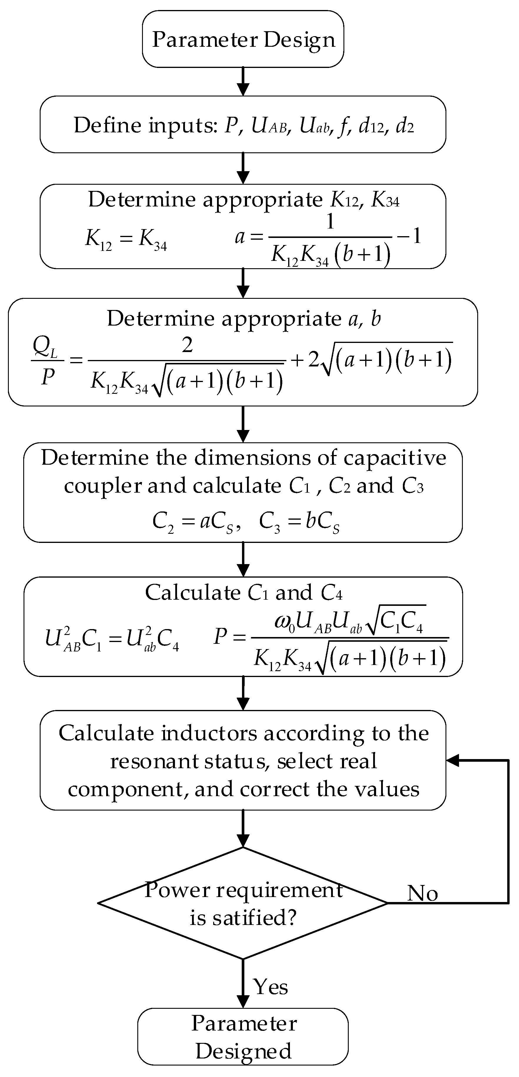
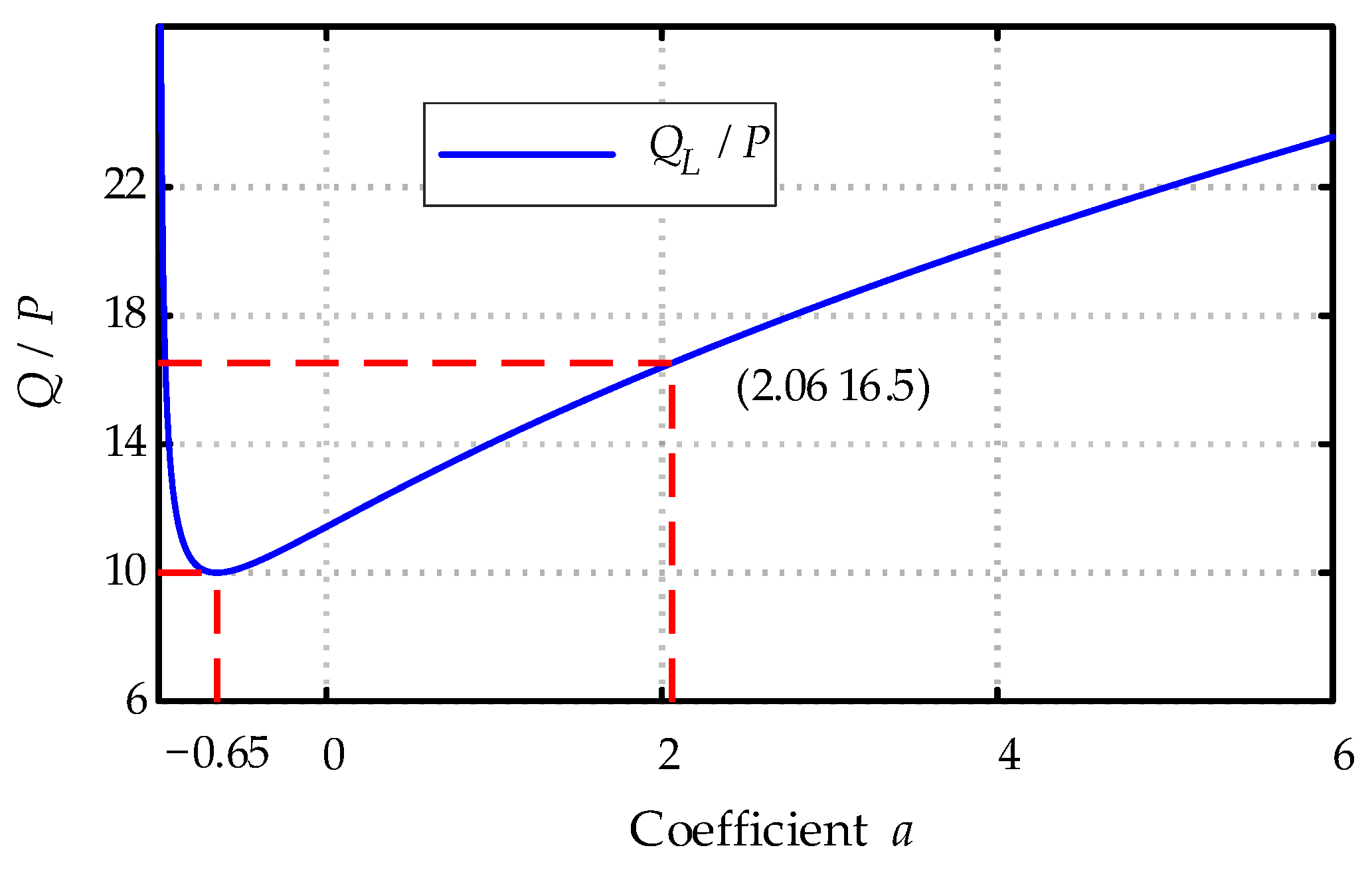
3.1. General Optimization Method Based on Equal Reactive Power

To minimize the optimization objective, the transferred power should be considered while minimizing the reactive power. Therefore, the transferred power can be seen as a constraint for the reduction of the reactive power. Since the total inductive reactive power was equal to the total capacitive reactive power, it was sufficient to minimize the inductive reactive power in this study.
In the CPT system, the reactive power is excited by the voltage sources UAB and Uab, which can be represented as QAB and Qab, respectively. From Equation (10), QAB and Qab can be expressed as
{ Q A B = ω 0 C 1 U A B 2 ( C S 2 K 12 2 K 34 2 ( C 3 + C S ) ( C 2 + C S ) + 1 K 12 2 ) Q a b = ω 0 C 4 U a b 2 ( C S 2 K 12 2 K 34 2 ( C 3 + C S ) ( C 2 + C S ) + 1 K 34 2 )
From Equations (10) and (16), the inductive reactive power can then be expressed as
Q L = Q A B + Q a b
In this study, the system parameters ω0, UAB, Uab, K12, K34, C1, C4, C2, C3, and CS are independent; they can be adjusted independently. Since the reactive powers QAB and Qab in the linear system are excited by the independent voltage sources UAB and Uab, QAB and Qab are independent. The relationship between the transferred power P and the reactive power QAB and Qab can then be expressed as
Q A B Q a b = P ( 1 K 34 K 12 ( C 3 C S + 1 ) ( C 2 C S + 1 ) + ( C 3 C S + 1 ) ( C 2 C S + 1 ) ) 2 + ( 1 K 12 1 K 34 ) 2
We can see from Equation (18) that when the transferred power is determined, the product of QAB and Qab has a minimum value. For each given product value of QAB and Qab, the total inductive reactive power has a minimum value, where
Q L 2 Q A B Q a b
The equal sign in Equation (18) is achieved when QAB and Qab are equal. Under the constraint of transferred power, it can be verified that equal QAB and Qab can be achieved. Here, we set the equal reactive powers QAB and Qab as a circuit condition. According to the equal reactive powers QAB and Qab, the total inductive reactive power can then be expressed as
Q L = 2 Q A B Q a b = 2 ω 0 U A B U a b C 1 C 4 ( C S 2 ( C 3 + C S ) ( C 2 + C S ) 1 K 12 2 K 34 2 + 1 K 12 2 ) ( C S 2 ( C 3 + C S ) ( C 2 + C S ) 1 K 12 2 K 34 2 + 1 K 34 2 )
where
U A B 2 C 1 ( C S 2 + K 34 2 ( C 3 + C S ) ( C 2 + C S ) ) = U a b 2 C 4 ( C S 2 + K 12 2 ( C 3 + C S ) ( C 2 + C S ) )
Considering the transferred power, the optimization objective can then be derived from Equations (6) and (20) as
Q L P = 2 1 K 12 2 + 1 K 34 2 + ( C 2 + C S ) ( C 3 + C S ) C S 2 + 1 K 12 2 K 34 2 C S 2 ( C 2 + C S ) ( C 3 + C S )
Furthermore, Equation (22) can be expressed as
Q L P = = 2 ( 1 K 34 K 12 ( C 3 C S + 1 ) ( C 2 C S + 1 ) + ( C 3 C S + 1 ) ( C 2 C S + 1 ) ) 2 + ( 1 K 12 1 K 34 ) 2
Since K12 and K34 are independent, their values can be adjusted independently. For each given value of K12 and K34, the optimization objective in Equation (23) can be further decreased when K12 and K34 are equal. In this case, Equation (23) can be changed to
Q L P = 2 K 12 K 34 ( C 3 C S + 1 ) ( C 2 C S + 1 ) + 2 ( C 3 C S + 1 ) ( C 2 C S + 1 )
where
K 12 = K 34
By substituting Equation (25) into Equation (21), the relationship between C1 and C4 can be obtained as
U A B 2 C 1 = U a b 2 C 4
In this study, an asymmetric six-plate capacitive coupler was used, where C2 < C3. To simplify the analysis, the coefficients a and b are used to describe the relationship between capacitors C2, C3 and CS, where
C 2 = a C S ,     C 3 = b C S
From Equations (27) and (24), the optimization objective can be derived as
Q L P = 2 K 12 K 34 ( a + 1 ) ( b + 1 ) + 2 ( a + 1 ) ( b + 1 )
When the value of b is determined, the minimized QL/P can be obtained. At the minimum value point, the value of a can be expressed as
a = 1 K 12 K 34 ( b + 1 ) 1
where
min Q L P = 4 K 12 K 34 = 4 K 12 = 4 K 34
We can see from Equation (30) that the minimum value of QL/P is just related to the coupling coefficients; by increasing the values of K12 and K34, the value of QL/P can be further decreased.
By substituting Equations (25) and (26) into Equation (6), the transferred power can be described as
P = ω 0 U A B U a b C 1 C 4 K 12 K 34 ( a + 1 ) ( b + 1 )
According to Equation (2), Equation (31) can be changed to
P = 8 ω 0 V i n V o u t C 1 C 4 π 2 K 12 K 34 ( a + 1 ) ( b + 1 )
From the above analysis, a general parameter optimization method that is based on equal reactive power can be obtained. Figure 6 shows the design flowchart. Considering the actual application scenarios, the system requirements are given and defined as inputs. The optimized coefficients K12, K34, a and b can be obtained by Equations (25), (28) and (29). Based on Equation (27), the relationship between the coupling capacitors can be derived. With the given airgap distances d12 and d2, an appropriate capacitive coupler with optimized coupling capacitors can be determined. According to Equations (26) and (27), the optimized C1 and C4 can be obtained. The resonant inductors can then be obtained by using the resonant conditions. Finally, the parameters can be adjusted iteratively depending on the available commercial inductors and capacitors.

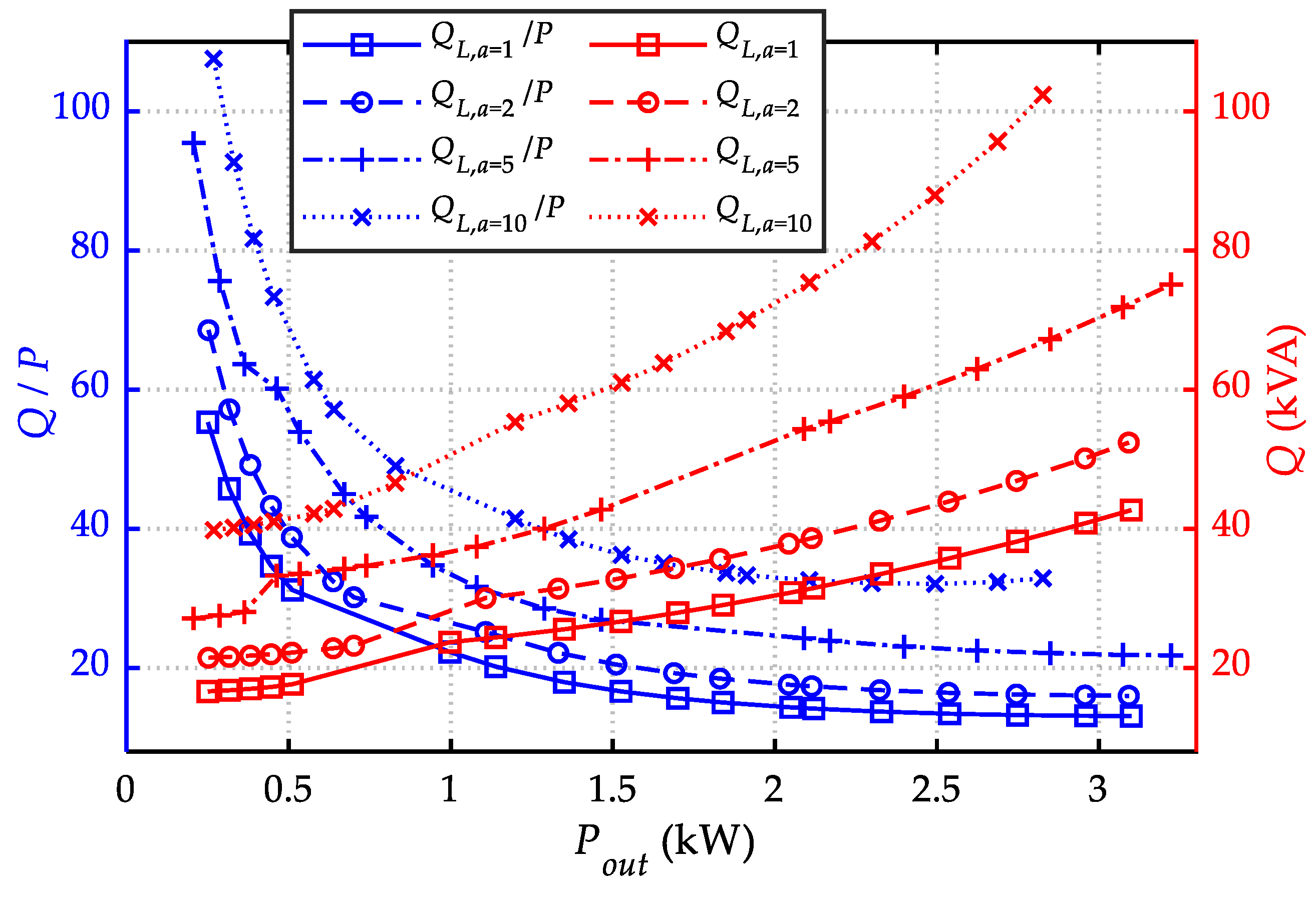
3.2. Comparation with the General Optimization Method

Both the two-stage optimization method [50] and the general optimization method that is proposed in this study aim to increase the system’s efficiency by optimizing the reactive power in the CPT system. The optimization objectives and optimization processes in the two methods are similar. The difference is that in the two-stage optimization method the capacitive coupler is first optimized and then the symmetric coupling parameters are verified to be an efficient configuration for the CPT system. The two-stage method is suitable for a CPT system with symmetric circuit parameters. In order to further the research, this paper studies the asymmetric CPT system and its general optimization method. Based on the properties of a linear CPT system, equal reactive power was used to optimize the reactive power in the CPT system. This method is suitable for both symmetric and asymmetric CPT systems. Besides this, when the coupling capacitors C2 and C3 were equal, the optimization results in the two studies were same.

4. Parameter Design and Implementation

Considering the actual requirements in EV wireless charging applications, a CPT prototype with an asymmetric coupling structure was implemented in order to validate the proposed method.

4.1. System Requirements
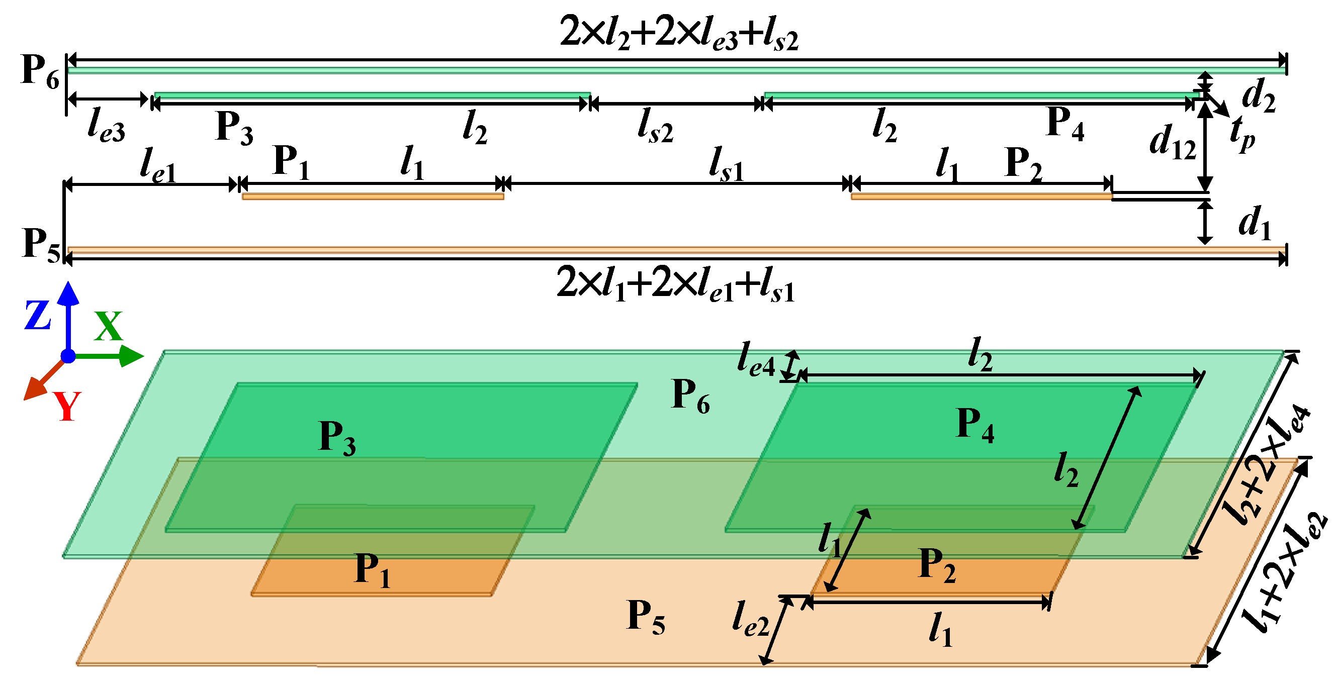
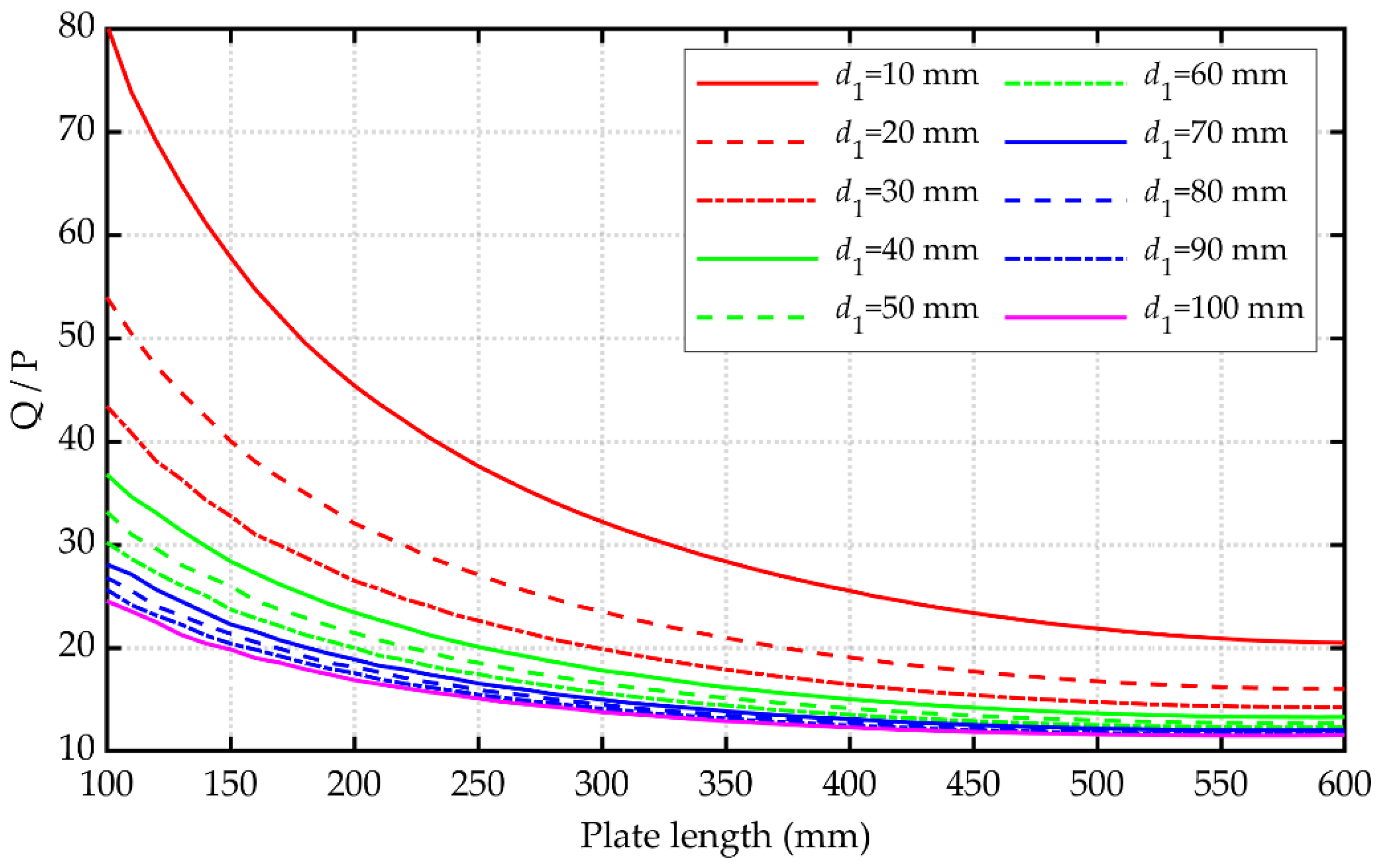
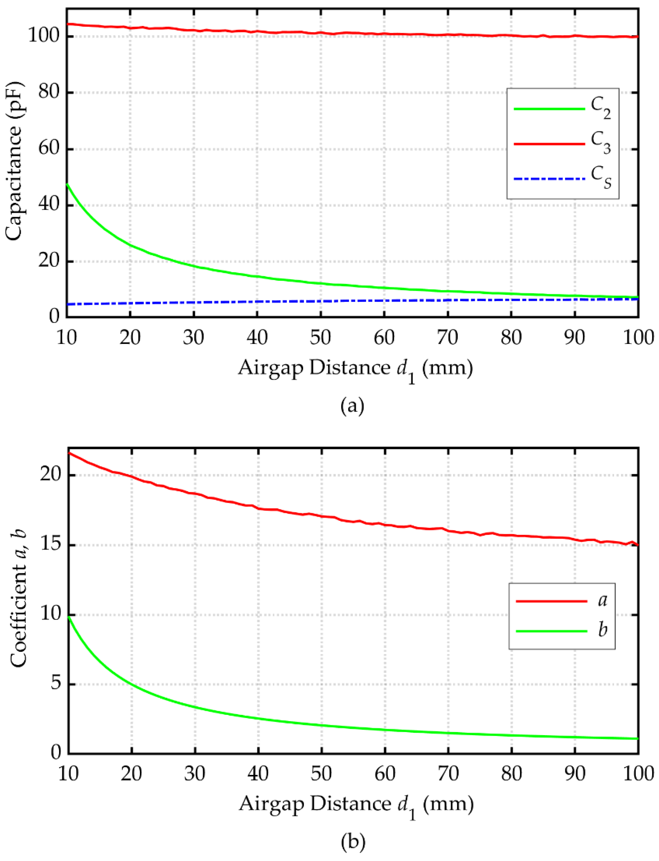
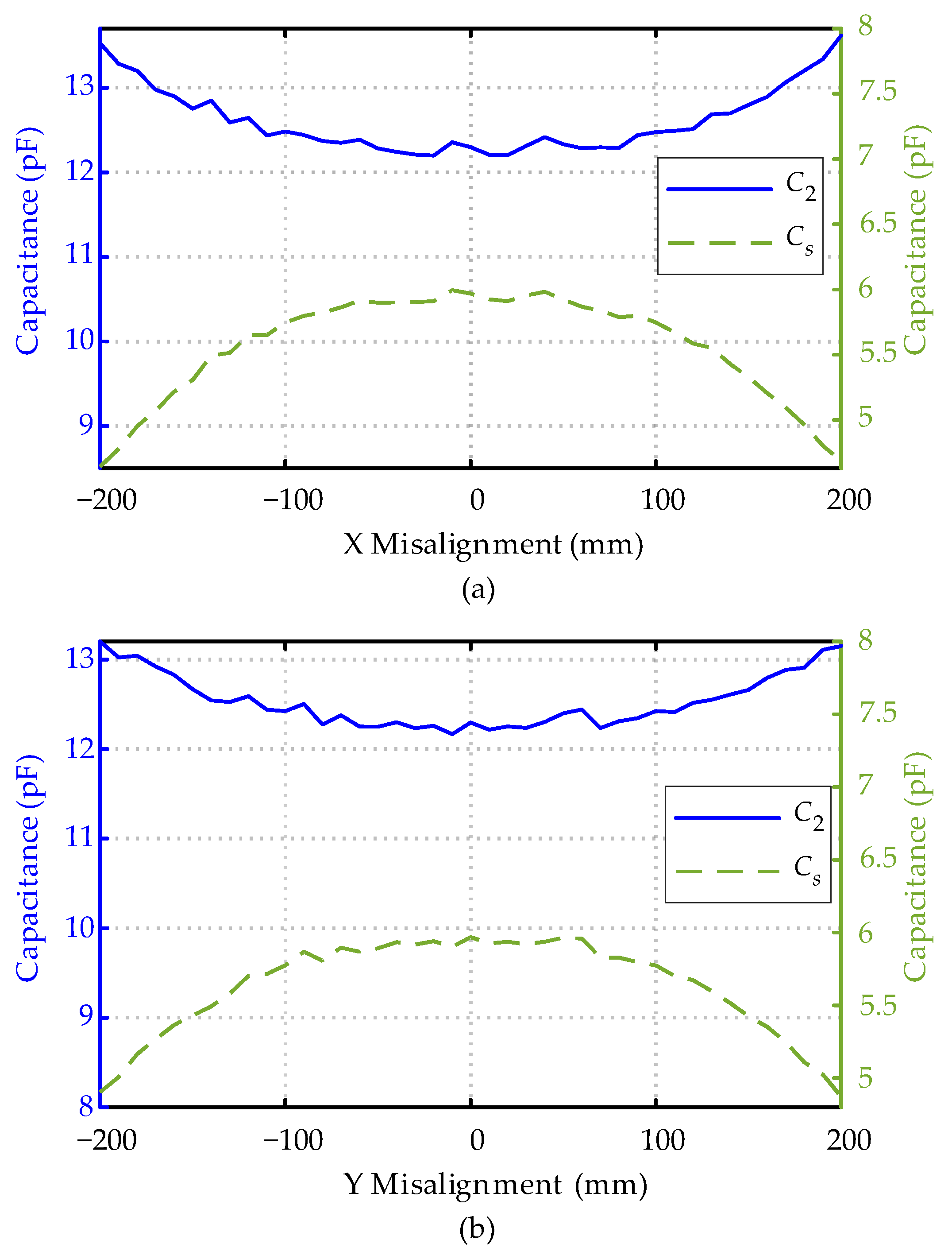
As shown in Table 1, the system requirements in an actual CPT system are given. To satisfy the requirements of the charging distance and passability, the transferred distance d12 was set to 100 mm. Since the installation space under the vehicle chassis was limited, the airgap distance d2 on the vehicle’s side was set to 20 mm. The operating frequency of the CPT system was 1 MHz. The transferred power was set to 3.2 kW and both the input and output voltages were set to 450 V.
We can see from Equations (28) and (30) that the optimization objective can be reduced by increasing the value of the coupling coefficients K12 and K34. However, studies have shown that a large third harmonic can be induced in the inverter when K12 and K34 are greater than 0.4 [62]. Therefore, the values of K12 and K34 were both set to 0.4 in this study.

4.2. Coupler Design

In this study, the asymmetric six-plate capacitive coupler was formed by 2 mm-thick aluminum plates. The structure is shown in Figure 7 and the dimensions of the designed coupler are shown in Table 2. The transmitting plates and receiving plates are square and centrosymmetric. On the receiving side, the plate length l2 was 600 mm, the shielding edges le3 and le4 were both 50 mm, and the plate separation ls2 was 100 mm. The distance d2 was 20 mm and the transmission distance d12 was 100 mm. The remaining dimensions of the transmitting side were plate length l1 and distance d1.
In order to obtain the appropriate plate length l1 and shielding distance d1, ANSYS Maxwell was used to simulate the coupling capacitors under different l1 and d1 values. According to Equation (24), the optimization objective under different values of l1 and d1 can then be obtained. The results are shown in Figure 8, where the ratio values decrease with increasing plate length l1 and airgap distance d1. Without a loss of generality, the plate length was set to 300 mm in this study in order to form an asymmetric capacitive coupler. With the defined l1, the plate separation ls2 and the shielding edges le1 and le2 could be obtained.
The only parameter that needed to be seriously considered was the gap distance d1. When other parameters are determined, the variation of d1 can affect the values of the coupling capacitances, which can be simulated by using ANSYS Maxwell. Figure 9 shows the simulated values of C2, C3, and CS and coefficients a and b under different values of airgap distance d1.
We can see from Figure 9a that the capacitance of C3 is greater than that of C2 and CS. With an increasing airgap distance d1, the values of C2 and C3 decrease, while CS increases slightly. As a result, both a and b decrease with increasing d1, as shown in Figure 9b. In Figure 10, the optimization objective under different distance d1 is calculated. To reduce the value of QL/P, the value of the gap distance d1 tends to be large. However, with a large d1, the value of C2 is very small, which enlarges the inductance values and makes the CPT system more sensitive to surrounding disturbances. Therefore, both QL/P and C2 should be considered in the selection of d1. To achieve an appropriate QL/P and avoid C2 being too small, d1 was set to 50 mm. Correspondingly, QL/P was set to 16.5, a was set to 2.06, b was set to 17.06, C2 was set to 12.25 pF, C3 was set to 101.5 pF, and CS was set to 5.95 pF.
It should be noted that when b is given, the theoretical minimum QL/P can be obtained from Equations (29) and (30). If we assume that the value of b does not change with the variation of a, the relationship between the ratio of QL/P and the coefficient a is shown in Figure 11. The minimum QL/P value of 10 can be achieved when the coefficient a is −0.65. To make the coefficient a higher than 0, the value of b should be less than 5.25.
Via the finite element simulation software ANASYS Maxwell, the performance of the capacitive coupler with the given parameters was simulated. Figure 12 shows the simulated capacitances C2 and CS under different X and Y misalignments. With an increasing misalignment condition, the simulated C2 values increase while the CS values decrease.

4.3. Resonant Parameter Design

With the given system parameters, the other resonant parameters can then be obtained. Considering the power losses in an actual system, the transferred power that is used to calculate the circuit parameters should be set slightly higher than the rated value. Based on Equations (6) and (31), the capacitances C1 and C4 can be calculated as.
{ C 1 = P K 12 K 34 ( a + 1 ) ( b + 1 ) ω 0 U A B 2 = 3400 0.4 0.4 ( 2.06 + 1 ) ( 17.06 + 1 ) 2 π 10 6 450 450 8 / π 2 = 3.92 n F C 4 = P K 12 K 34 ( a + 1 ) ( b + 1 ) ω 0 U a b 2 = 3400 0.4 0.4 ( 2.06 + 1 ) ( 17.06 + 1 ) 2 π 10 6 450 450 8 / π 2 = 3.92 n F
The resonant inductors L1, L2, L3, and L4 can be obtained based on the following resonant relationship:
ω 0 = 2 π f = 1 / L 1 C 1 = 1 / L 4 C 4 = 1 / L 2 ( C 2 + C 3 C S C 3 + C S ) = 1 / L 3 ( C 3 + C 2 C S C 2 + C S )
The designed system’s parameters are shown in Table 3. It should be noted that the parasitic capacitance between the windings of the inductors is inevitable and should not be eliminated in this study. The structure of the actual inductor is shown in Figure 13. Generally, the parallel-connected parasitic capacitance in the inductors is very small (usually in the range of several picofarads), which is close to the capacitance values of C2 and CS. As a result, the resonant inductors L2 and L3 deviated from the design values. Besides this, the metal plates were deformed due to the influence of gravity, resulting in a small variation of the coupling capacitance CS. Considering the actual value of the ceramic capacitors and the effect of parasitic capacitances in the inductors, C1 and C4 were adjusted to 4.2 nF. To avoid measurement errors, the parameters were tuned by using a network analyzer.

5. Simulation and Experimental Results

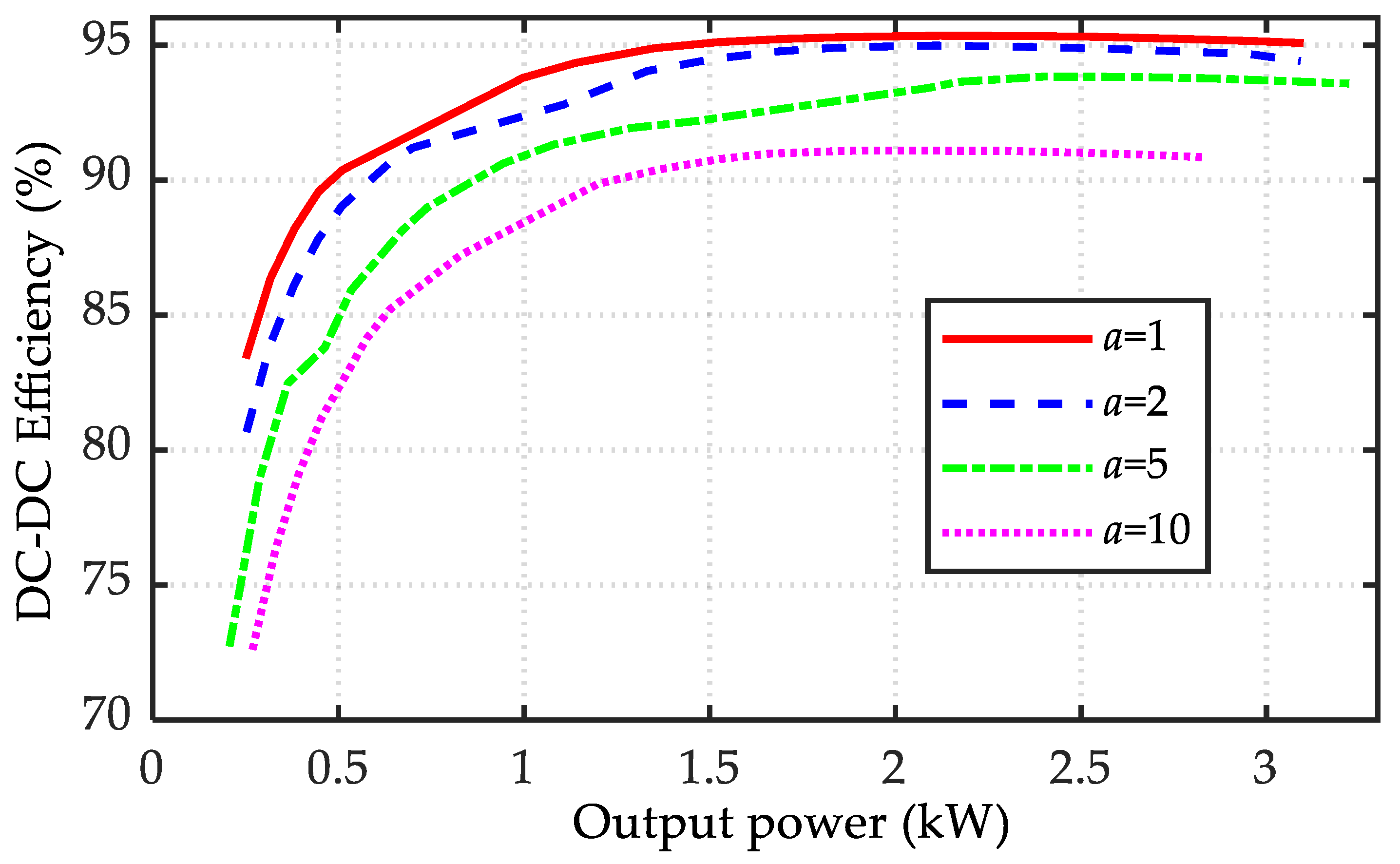
5.1. Simulation Results

In this study, the system’s performance was simulated by using LTspice. The circuit that is shown in Figure 4 was used to model the proposed CPT system. The simulation’s results are shown in Figure 14, Figure 15 and Figure 16. The waveforms of the voltages UC2 and UC3, input current, and voltage (I1 and UAB) are shown in Figure 14. Due to the asymmetric configuration of the CPT system, the rms values of UC2 are greater than those of UC3. The phase difference between UC2 and UC3 is about 78°. The phases of the current and voltage on the input side are almost identical, which allowed the system to operate at high-power factor conditions.
The simulated values of QL and QL/P under different values of the coefficient a are shown in Figure 15. The results show that the reactive power increases with increasing output power and coefficient a value and the ratio of QL/P increases with increasing coefficient a value and decreases with increasing output power. In this study, the coefficient a was set to 2, and the value of QL/P at the rated power was approximately 17, which agrees well with the designed value.
The system efficiency under different values of the coefficient a was simulated and the results are displayed in Figure 16. The results show that the system efficiency increased with increasing output power and it decreased with increasing values of the coefficient a. The trend of system efficiency in Figure 15 is opposite to that of QL/P in Figure 15, which agrees well with the analysis.
The voltages between the plates in the CPT system with different values of coefficient a were also analyzed. By using the proposed method, the system parameters under different values of a can be obtained. The voltages between the plates at the rated power can then be calculated as shown in Table 4. The voltages between the shielding plates (P5 and P6) were almost 0, which shows a good shielding effect in this design. Since the circuit parameters in designed CPT system were asymmetric, the voltages between the plates in the primary and secondary side were different. The voltages between the transmitting plates (P1 and P2) were higher than those which were observed between the receiving plates (P3 and P4). When the value of a increased from 1 to 10, the voltages between the plates in the transmitting side (P1, P2, and P5) decreased, while in the receiving side (P3, P4, and P6) the voltages increased. Besides this, the voltages between the transmission plates (P1 and P3) decreased with the increasing value of a. In this study, the voltage between P1 and P5 was approximately 7.56 kV. There was no risk of arcing [48] because the airgap distance between the plates was large.

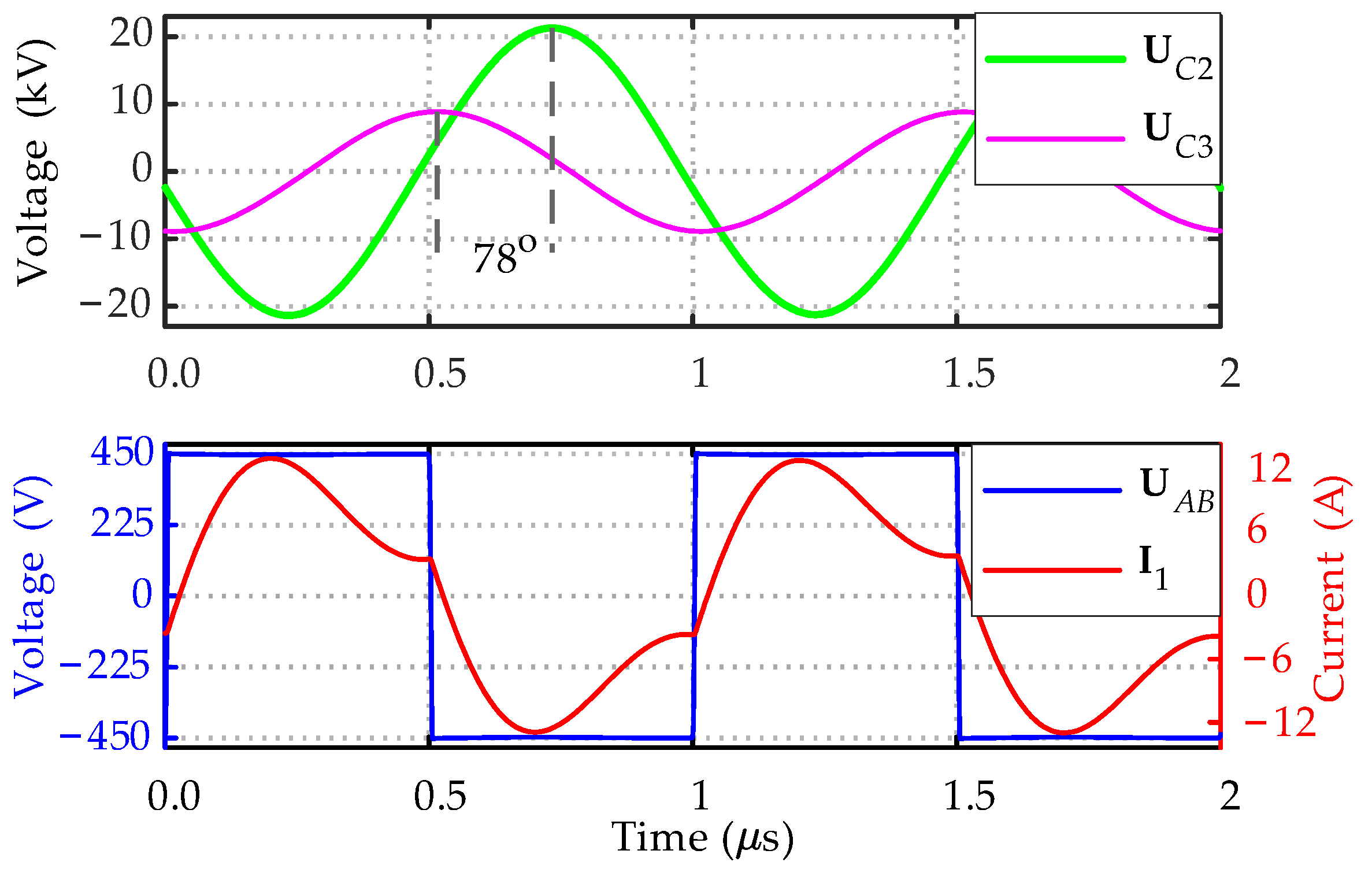
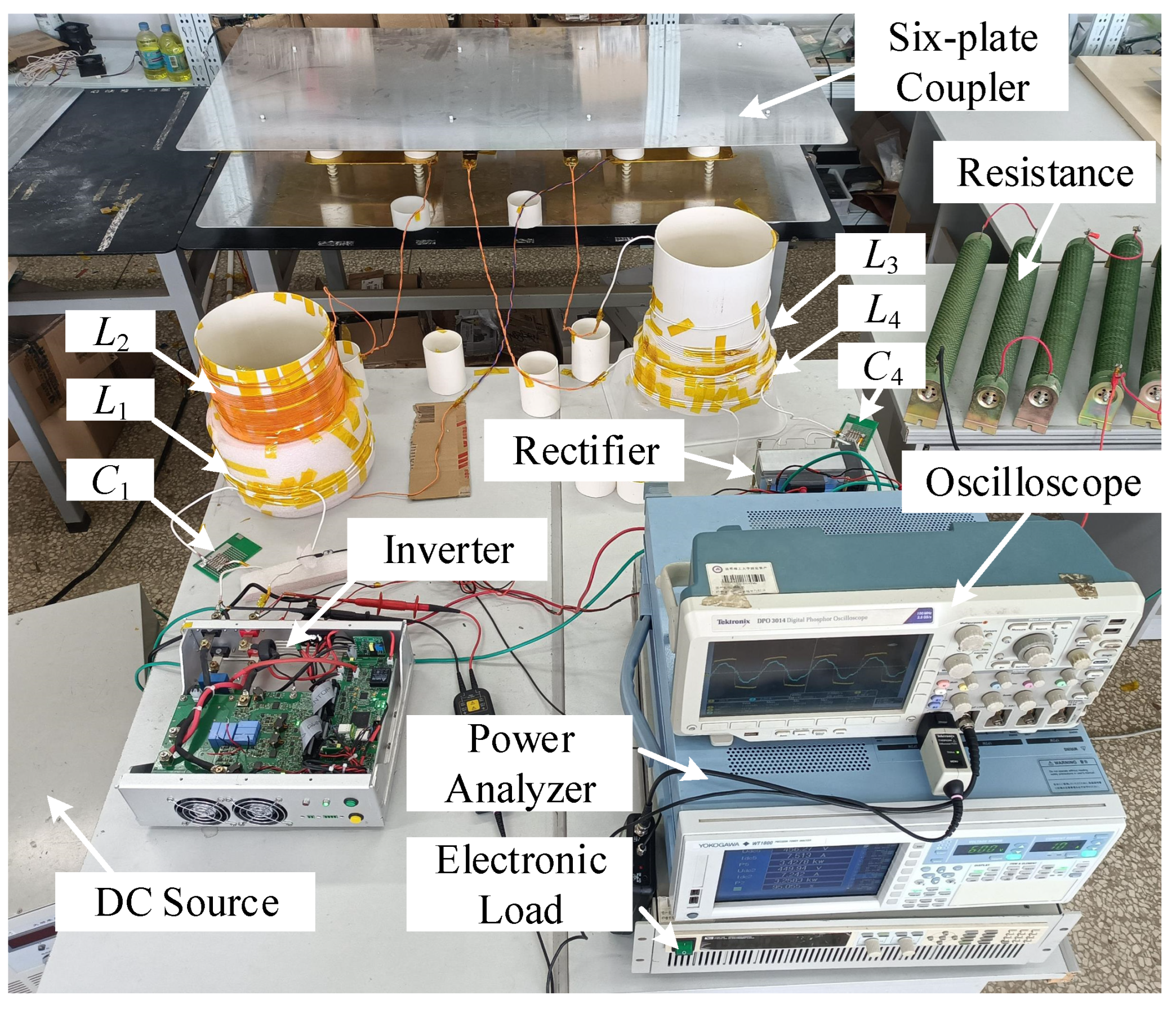
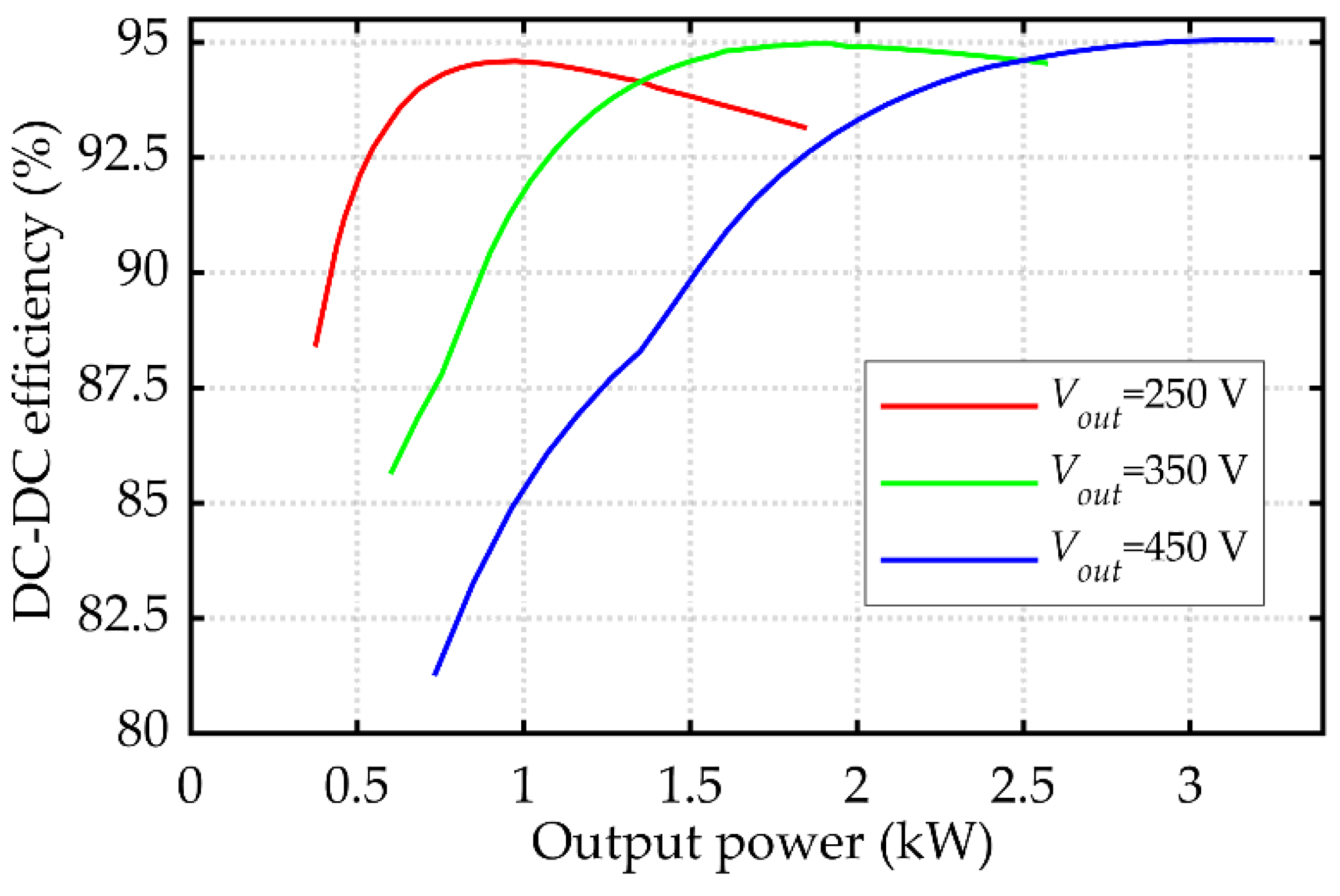
5.2. Experimental Verification

To verify the proposed method, a 3.2-kW CPT prototype was built as shown in Figure 17. The asymmetric capacitive coupler with a large receiver and small transmitter was made up of six aluminum plates. The plates were held by PVC tubes and ceramic insulators and the outside shielding plates were floating. Under the capacitive coupler, a black steel plate was used as the ground. The mutual capacitance was 6.75 pF and the transferred distance was 100 mm. Just like the schematic circuit that is shown in Figure 4, a DC power source was used in order to provide a DC voltage to the inverter on the transmitting side of this prototype. An electric DC load, together with several parallel-connected resistors, was used as the load and connected to the rectifier on the receiving side. The power converters were formed by SiC devices IMZ120R045M1 and IDW40G120C5B. The inductors L1L4 were wound onto the PVC tubes with 1200-strand Litz wire with a diameter of 0.04 mm, which allowed easy adjustment of the coupling coefficients K12 and K34. The compensation capacitors consisted of high voltage, low dissipation factor ceramic capacitors.
From the designed prototype, the experimental results at the rated power are shown in Figure 18 and Figure 19. The plates in the coupler were well aligned. In order to reduce the switching losses and improve the system’s efficiency, zero-voltage turn-on should be achieved for the switching devices. By slightly reducing the value of inductor L2, the ZVS condition was realized, as shown in Figure 18a,b. The waveforms of the input voltage and current were almost in phase and the ZVS condition was achieved by a phase shift of the input current. At the rated input and output DC voltages, about 3.2 kW power was delivered from the DC source to the electric DC load and resistors with an efficiency of 95%. The transmission efficiency under different output power is shown in the Figure 19. With different output voltages, the maximum system efficiencies were both higher than 94.5%.
The comparison between the presently designed CPT system and the previous published CPT systems that have a large airgap distance and kilowatt-scale power is shown in Table 5. The DC–DC overall efficiency is considered. As shown in Table 5, the airgap and coupling area that were used in this study are small, resulting in a lower volume and coupling capacitance. When the element numbers of the systems are similar, the designed CPT system can achieve high transmission efficiency with a relatively low coupling capacitance.
The power loss distribution of the presently designed system was analyzed. According to the calculation method that was proposed in [44,63,64], the power losses in the MOSFETs, diodes, inductors, and capacitors were obtained. Based on the on-resistance and switching-off current, the losses in the switching devices could then be calculated; the losses in the inductors and capacitors were obtained from the measured quality factors. The remaining losses are from within the coupling plates. As shown in Figure 20, the inductors and capacitive coupler dissipate 39.2% and 33.6% of the total loss, respectively, which makes up the main losses of the system.

6. Conclusions

A general parameter optimization method for an asymmetric CPT system is proposed in this article. A six-plate capacitive coupler with an asymmetric structure was used and compensated by an EFR compensation circuit. The asymmetric coupler structure was analyzed and the whole system was modeled. The relationship between the transferred power and reactive power was analyzed. Based on the properties of a linear CPT system, an optimization method was proposed. By using the equal reactive power, the circuit conditions that are required in order to optimize the reactive power were obtained. With these circuit conditions, the reactive power was simplified and the circuit parameters were optimized. Based on the optimization process, a general parameter optimization method was proposed and implemented on a 3.2-kW, 1 MHz CPT protype. Both the simulated and experimental results show that, with the proposed method, high system efficiency can be achieved for an asymmetric CPT system with low coupling capacitance. About 3.2 kW of power was transferred with a DC–DC efficiency of 95%. Although the special compensation topology and an asymmetric coupler were used in this study, the proposed method is not limited to this topology and it is suitable for both symmetric and asymmetric CPT systems.

Author Contributions

Article outline, X.Y. and S.L. (Siqi Li), conceptualization and methodology, J.X., X.Y. and S.L. (Siqi Li); investigation, J.X., W.D. and T.L.; formal analysis and writing—original draft preparation, J.X.; writing—review and editing, S.L. (Sizhao Lu), X.Y. and J.L. All authors have read and agreed to the published version of the manuscript.

Funding

This work was supported in part by the National Natural Science Foundation of China under Grant 51607081 and in part by the National Key Research and Development Plan under Grant 2017YFB0103203.

Conflicts of Interest

The authors declare no conflict of interest.

Appendix A

The conditions under which CPT systems have different quality factors are analyzed in Appendix A. According to the analysis that was presented in Section 2.4, when other parameters are determined, the transmission efficiency of the CPT system is dependent on the reactive power and quality factors of the circuit components. With unequal quality factors applied on the circuit components, the optimization objective expression in the study can then be changed to
Q L j Q L j * P + Q C i Q C i * P     ( j = 1 , 2 , 3 , 4 ; i = S , 1 , 2 , 3 , 4 ) .
When a CPT system is built, the quality factors of the circuit components are determined. Here, the quality factors can be seen as independent from each other. Since the quality factors do not affect the independence of the system parameters, the properties of linear CPT system can also be used to reduce the complexity of the optimization objective. The difference is that, with unequal quality factors, the circuit conditions that are obtained to simplify the optimization objective contain unequal quality factors.
The parameter optimization design process for a CPT system with unequal quality factors is similar to that of one with equal quality factors. Therefore, we just demonstrate the optimization of a CPT system with equal quality factors in this article.

References

  1. Yang, Y.; El Baghdadi, M.; Lan, Y.; Benomar, Y.; Van Mierlo, J.; Hegazy, O. Design Methodology, Modeling, and Comparative Study of Wireless Power Transfer Systems for Electric Vehicles. Energies 2018, 11, 1716. [Google Scholar] [CrossRef] [Green Version]
  2. Rahmani, F.; Niknejad, P.; Agarwal, T.; Barzegaran, M. Gallium Nitride Inverter Design with Compatible Snubber Circuits for Implementing Wireless Charging of Electric Vehicle Batteries. Machines 2020, 8, 56. [Google Scholar] [CrossRef]
  3. Li, S.; Lu, S.; Mi, C.C. Revolution of Electric Vehicle Charging Technologies Accelerated by Wide Bandgap Devices. Proc. IEEE 2021, 109, 985–1003. [Google Scholar] [CrossRef]
  4. Dai, J.; Ludois, D.C. A Survey of Wireless Power Transfer and a Critical Comparison of Inductive and Capacitive Coupling for Small Gap Applications. IEEE Trans. Power Electron. 2015, 30, 6017–6029. [Google Scholar] [CrossRef]
  5. Lu, F.; Zhang, H.; Mi, C. A Review on the Recent Development of Capacitive Wireless Power Transfer Technology. Energies 2017, 10, 1752. [Google Scholar] [CrossRef] [Green Version]
  6. Li, S.; Mi, C.C. Wireless Power Transfer for Electric Vehicle Applications. IEEE J. Emerg. Sel. Top. Power Electron. 2014, 3, 4–17. [Google Scholar]
  7. Zhang, Z.; Pang, H.; Georgiadis, A.; Cecati, C. Wireless Power Transfer—An Overview. IEEE Trans. Ind. Electron. 2019, 66, 1044–1058. [Google Scholar] [CrossRef]
  8. Nguyen, V.T.; Kang, S.H.; Choi, J.H.; Jung, C.W. Magnetic Resonance Wireless Power Transfer Using Three-Coil System with Single Planar Receiver for Laptop Applications. IEEE Trans. Consumer Electron. 2015, 61, 160–166. [Google Scholar] [CrossRef]
  9. Madhja, A.; Nikoletseas, S.; Voudouris, A.A. Adaptive Wireless Power Transfer in Mobile Ad Hoc Networks. Comput. Netw. 2019, 152, 87–97. [Google Scholar] [CrossRef] [Green Version]
  10. Hu, A.P.; Liu, C.; Li, H.L. A Novel Contactless Battery Charging System for Soccer Playing Robot. In Proceedings of the 2008 15th International Conference on Mechatronics and Machine Vision in Practice, Auckland, New Zealand, 2–4 December 2008; pp. 646–650. [Google Scholar]
  11. Culurciello, E.; Andreou, A.G. Capacitive Inter-Chip Data and Power Transfer for 3-D VLSI. IEEE Trans. Circuits Syst. II Express Briefs 2006, 53, 1348–1352. [Google Scholar] [CrossRef]
  12. Jiang, C.; Chau, K.T.; Ching, T.W.; Liu, C.; Han, W. Time-Division Multiplexing Wireless Power Transfer for Separately Excited DC Motor Drives. IEEE Trans. Magn. 2017, 53, 1–5. [Google Scholar] [CrossRef]
  13. Raval, P.; Kacprzak, D.; Hu, A.P. A Multi-Phase 3D Inductive Power Transfer System Based on a Rotating Magnetic Field. IEEE Trans. Ind. Electron. 2015, 62, 795–802. [Google Scholar] [CrossRef]
  14. Ludois, D.C.; Reed, J.K.; Hanson, K. Capacitive Power Transfer for Rotor Field Current in Synchronous Machines. IEEE Trans. Power Electron. 2012, 27, 4638–4645. [Google Scholar] [CrossRef]
  15. Zhou, Y.; Liu, C.; Huang, Y. Wireless Power Transfer for Implanted Medical Application: A Review. Energies 2020, 13, 2837. [Google Scholar] [CrossRef]
  16. Li, L.; Liu, H.; Zhang, H.; Xue, W. Efficient Wireless Power Transfer System Integrating with Metasurface for Biological Applications. IEEE Trans. Ind. Electron. 2018, 65, 3230–3239. [Google Scholar] [CrossRef]
  17. Hu, A.P.; You, Y.W.; Chen, F.-Y.B.; McCormick, D.; Budgett, D.M. Wireless Power Supply for ICP Devices with Hybrid Supercapacitor and Battery Storage. IEEE J. Emerg. Sel. Top. Power Electron. 2016, 4, 273–279. [Google Scholar] [CrossRef]
  18. Palagani, Y.; Mohanarangam, K.; Shim, J.H.; Choi, J.R. Wireless Power Transfer Analysis of Circular and Spherical Coils under Misalignment Conditions for Biomedical Implants. Biosens. Bioelectron. 2019, 141, 111283. [Google Scholar] [CrossRef]
  19. Sodagar, A.M.; Amiri, P. Capacitive Coupling for Power and Data Telemetry to Implantable Biomedical Microsystems. In Proceedings of the 2009 4th International IEEE/EMBS Conference on Neural Engineering, Antalya, Turkey, 29 April–2 May 2009; pp. 411–414. [Google Scholar]
  20. Deng, J.; Pang, B.; Shi, W.; Wang, Z. A New Integration Method with Minimized Extra Coupling Effects Using Inductor and Capacitor Series-Parallel Compensation for Wireless EV Charger. Appl. Energy 2017, 207, 405–416. [Google Scholar] [CrossRef]
  21. Zhao, L.; Thrimawithana, D.; Madawala, U.; Hu, A.; Mi, C. A Misalignment-Tolerant Series-Hybrid Wireless EV Charging System with Integrated Magnetics. IEEE Trans. Power Electron. 2018, 34, 1276–1285. [Google Scholar] [CrossRef]
  22. Zhou, S.; Chris Mi, C. Multi-Paralleled LCC Reactive Power Compensation Networks and Their Tuning Method for Electric Vehicle Dynamic Wireless Charging. IEEE Trans. Ind. Electron. 2016, 63, 6546–6556. [Google Scholar] [CrossRef]
  23. Lu, F. High Power Capacitive Power Transfer for Electric Vehicle Charging Applications. Ph.D. Dissertation, University Michigan, Ann Arbor, MI, USA, 2017. [Google Scholar]
  24. Lu, F.; Zhang, H.; Mi, C. A Two-Plate Capacitive Wireless Power Transfer System for Electric Vehicle Charging Applications. IEEE Trans. Power Electron. 2018, 33, 964–969. [Google Scholar] [CrossRef]
  25. Lu, F.; Zhang, H.; Hofmann, H.; Mi, C. A Double-Sided LCLC-Compensated Capacitive Power Transfer System for Electric Vehicle Charging. IEEE Trans. Power Electron. 2015, 30, 6011–6014. [Google Scholar] [CrossRef]
  26. Mohamed, A.A.; Shaier, A.A.; Metwally, H.; Selem, S.I. A Comprehensive Overview of Inductive Pad in Electric Vehicles Stationary Charging. Appl. Energy 2020, 262, 114584. [Google Scholar] [CrossRef]
  27. Lu, F.; Mi, C.C. An Inductive and Capacitive Combined Wireless Power Transfer System with LC-Compensated Topology. IEEE Trans. Power Electron. 2016, 31, 12. [Google Scholar] [CrossRef]
  28. Rituraj, G.; Joy, E.R.; Kushwaha, B.K.; Kumar, P. Analysis and Comparison of Series-Series and Series-Parallel Topology of Contactless Power Transfer Systems. In Proceedings of the TENCON 2014–2014 IEEE Region 10 Conference, Bangkok, Thailand, 22–25 October 2014; pp. 1–6. [Google Scholar]
  29. Zahid, Z.U.; Dalala, Z.M.; Zheng, Z.; Chen, R.; Faraci, W.E.; Lai, J.-S.J.; Lisi, G.; Anderson, D. Modeling and Control of Series–Series Compensated Inductive Power Transfer System. IEEE J. Emerg. Sel. Top. Power Electron. 2015, 3, 111–123. [Google Scholar] [CrossRef]
  30. Zhang, W.; Mi, C.C. Compensation Topologies of High-Power Wireless Power Transfer Systems. IEEE Trans. Veh. Technol. 2016, 65, 4768–4778. [Google Scholar] [CrossRef]
  31. Li, S.; Li, W.; Deng, J.; Nguyen, T.D.; Mi, C.C. A Double-Sided LCC Compensation Network and Its Tuning Method for Wireless Power Transfer. IEEE Trans. Veh. Technol. 2015, 64, 2261–2273. [Google Scholar] [CrossRef]
  32. Lu, F.; Zhang, H.; Hofmann, H.; Su, W.; Mi, C.C. A Dual-Coupled LCC-Compensated IPT System with a Compact Magnetic Coupler. IEEE Trans. Power Electron. 2018, 33, 6391–6402. [Google Scholar] [CrossRef]
  33. Hou, J.; Chen, Q.; Zhang, Z.; Wong, S.-C.; Tse, C.K. Analysis of Output Current Characteristics for Higher Order Primary Compensation in Inductive Power Transfer Systems. IEEE Trans. Power Electron. 2018, 33, 6807–6821. [Google Scholar] [CrossRef]
  34. Hou, J.; Chen, Q.; Wong, S.-C.; Tse, C.K.; Ruan, X. Analysis and Control of Series/Series-Parallel Compensated Resonant Converter for Contactless Power Transfer. IEEE J. Emerg. Sel. Top. Power Electron. 2015, 3, 124–136. [Google Scholar] [CrossRef]
  35. Hou, J.; Chen, Q.; Ren, X.; Ruan, X.; Wong, S.-C.; Tse, C.K. Precise Characteristics Analysis of Series/Series-Parallel Compensated Contactless Resonant Converter. IEEE J. Emerg. Sel. Top. Power Electron. 2015, 3, 101–110. [Google Scholar] [CrossRef]
  36. Villa, J.L.; Sallan, J.; Sanz Osorio, J.F.; Llombart, A. High-Misalignment Tolerant Compensation Topology For ICPT Systems. IEEE Trans. Ind. Electron. 2012, 59, 945–951. [Google Scholar] [CrossRef]
  37. Lu, J.; Zhu, G.; Lin, D.; Zhang, Y.; Wang, H.; Mi, C.C. Realizing Constant Current and Constant Voltage Outputs and Input Zero Phase Angle of Wireless Power Transfer Systems with Minimum Component Counts. IEEE Trans. Intell. Transp. Syst. 2021, 22, 600–610. [Google Scholar] [CrossRef]
  38. Qu, X.; Jing, Y.; Han, H.; Wong, S.-C.; Tse, C.K. Higher Order Compensation for Inductive-Power-Transfer Converters with Constant-Voltage or Constant-Current Output Combating Transformer Parameter Constraints. IEEE Trans. Power Electron. 2017, 32, 394–405. [Google Scholar] [CrossRef]
  39. Qin, R.; Li, J.; Costinett, D. A 6.6-KW High Frequency Wireless Power Transfer System for Electric Vehicle Charging Using Multi-Layer Non-Uniform Self-Resonant Coil at MHz. IEEE Trans. Power Electron. 2021, 37, 4842–4856. [Google Scholar] [CrossRef]
  40. Li, L.; Wang, Z.; Gao, F.; Wang, S.; Deng, J. A Family of Compensation Topologies for Capacitive Power Transfer Converters for Wireless Electric Vehicle Charger. Appl. Energy 2020, 260, 114156. [Google Scholar] [CrossRef]
  41. Zou, Y.; Zhu, J.; Wang, X.; Hanzo, L. A Survey on Wireless Security: Technical Challenges, Recent Advances, and Future Trends. Proc. IEEE 2016, 104, 1727–1765. [Google Scholar] [CrossRef] [Green Version]
  42. Ludois, D.C.; Erickson, M.J.; Reed, J.K. Aerodynamic Fluid Bearings for Translational and Rotating Capacitors in Noncontact Capacitive Power Transfer Systems. IEEE Trans. Ind. Appl. 2014, 50, 1025–1033. [Google Scholar] [CrossRef]
  43. Zhu, Q.; Zou, L.J.; Su, M.; Hu, A.P. Four-Plate Capacitive Power Transfer System with Different Grounding Connections. Int. J. Electr. Power Energy Syst. 2020, 115, 105494. [Google Scholar] [CrossRef]
  44. Zhang, H.; Lu, F.; Hofmann, H.; Liu, W.; Mi, C.C. A Four-Plate Compact Capacitive Coupler Design and LCL-Compensated Topology for Capacitive Power Transfer in Electric Vehicle Charging Application. IEEE Trans. Power Electron. 2016, 31, 8541–8551. [Google Scholar] [CrossRef]
  45. Liu, Y.; Wu, T.; Fu, M. Interleaved Capacitive Coupler for Wireless Power Transfer. IEEE Trans. Power Electron. 2021, 36, 13526–13535. [Google Scholar] [CrossRef]
  46. Zhang, H.; Lu, F. An Improved Design Methodology of the Double-Sided LC -Compensated CPT System Considering the Inductance Detuning. IEEE Trans. Power Electron. 2019, 34, 11396–11406. [Google Scholar] [CrossRef]
  47. Wang, Y.; Zhang, H.; Lu, F. Capacitive Power Transfer with Series-Parallel Compensation for Step-Up Voltage Output. IEEE Trans. Ind. Electron. 2021, 69, 5604–5614. [Google Scholar] [CrossRef]
  48. Zhang, H.; Lu, F.; Hofmann, H.; Liu, W.; Mi, C.C. Six-Plate Capacitive Coupler to Reduce Electric Field Emission in Large Air-Gap Capacitive Power Transfer. IEEE Trans. Power Electron. 2018, 33, 665–675. [Google Scholar] [CrossRef]
  49. Li, S.; Liu, Z.; Zhao, H.; Zhu, L.; Shuai, C.; Chen, Z. Wireless Power Transfer by Electric Field Resonance and Its Application in Dynamic Charging. IEEE Trans. Ind. Electron. 2016, 63, 6602–6612. [Google Scholar] [CrossRef]
  50. Xia, J.; Yuan, X.; Lu, S.; Li, J.; Luo, S.; Li, S. A Two-Stage Parameter Optimization Method for Capacitive Power Transfer Systems. IEEE Trans. Power Electron. 2022, 37, 1102–1117. [Google Scholar] [CrossRef]
  51. Lu, F.; Zhang, H.; Hofmann, H.; Mi, C. A CLLC-Compensated High Power and Large Air-Gap Capacitive Power Transfer System for Electric Vehicle Charging Applications. In Proceedings of the 2016 IEEE Applied Power Electronics Conference and Exposition (APEC), IEEE, Long Beach, CA, USA, 20–24 March 2016; pp. 1721–1725. [Google Scholar]
  52. Sinha, S.; Kumar, A.; Afridi, K.K. Improved Design Optimization of Efficient Matching Networks for Capacitive Wireless Power Transfer Systems. In Proceedings of the 2018 IEEE Applied Power Electronics Conference and Exposition (APEC), San Antonio, TX, USA, 4–8 March 2018; pp. 3167–3173. [Google Scholar]
  53. Sinha, S.; Kumar, A.; Regensburger, B.; Afridi, K.K. Design of High-Efficiency Matching Networks for Capacitive Wireless Power Transfer Systems. IEEE J. Emerg. Sel. Top. Power Electron. 2020, 10, 104–127. [Google Scholar] [CrossRef]
  54. Kumar, A.; Sinha, S.; Sepahvand, A.; Afridi, K.K. Improved Design Optimization Approach for High Efficiency Matching Networks. In Proceedings of the 2016 IEEE Energy Conversion Congress and Exposition (ECCE), Milwaukee, WI, USA, 18–22 September 2016; pp. 1–7. [Google Scholar]
  55. Sinha, S.; Kumar, A.; Pervaiz, S.; Regensburger, B.; Afridi, K.K. Design of Efficient Matching Networks for Capacitive Wireless Power Transfer Systems. In Proceedings of the 2016 IEEE 17th Workshop on Control and Modeling for Power Electronics (COMPEL), Trondheim, Norway, 27–30 June 2016; pp. 1–7. [Google Scholar]
  56. Kumar, A.; Sinha, S.; Sepahvand, A.; Afridi, K.K. Improved Design Optimization for High-Efficiency Matching Networks. IEEE Trans. Power Electron. 2018, 33, 37–50. [Google Scholar] [CrossRef]
  57. Kim, T.-H.; Yun, G.-H.; Lee, W.Y.; Yook, J.-G. Asymmetric Coil Structures for Highly Efficient Wireless Power Transfer Systems. IEEE Trans. Microw. Theory Tech. 2018, 66, 3443–3451. [Google Scholar] [CrossRef]
  58. Nguyen, M.T.; Nguyen, C.V.; Truong, L.H.; Le, A.M.; Quyen, T.V.; Masaracchia, A.; Teague, K.A. Electromagnetic Field Based WPT Technologies for UAVs: A Comprehensive Survey. Electronics 2020, 9, 461. [Google Scholar] [CrossRef] [Green Version]
  59. Cai, C.; Wang, J.; Nie, H.; Zhang, P.; Lin, Z.; Zhou, Y.-G. Effective-Configuration WPT Systems for Drones Charging Area Extension Featuring Quasi-Uniform Magnetic Coupling. IEEE Trans. Transp. Electrif. 2020, 6, 920–934. [Google Scholar] [CrossRef]
  60. Zhu, Q.; Zhang, Y.; Liao, C.; Guo, Y.; Wang, L.; Li, F. Experimental Study on Asymmetric Wireless Power Transfer System for Electric Vehicle Considering Ferrous Chassis. IEEE Trans. Transp. Electrif. 2017, 3, 427–433. [Google Scholar] [CrossRef]
  61. Moon, S.; Moon, G.-W. Wireless Power Transfer System with an Asymmetric Four-Coil Resonator for Electric Vehicle Battery Chargers. IEEE Trans. Power Electron. 2016, 31, 6844–6854. [Google Scholar] [CrossRef]
  62. Luo, S.; Li, S.; Zhao, H. Reactive Power Comparison of Four-Coil, LCC and CLC Compensation Network for Wireless Power Transfer. In Proceedings of the 2017 IEEE PELS Workshop on Emerging Technologies: Wireless Power Transfer (WoW), Chongqing, China, 20–22 May 2017; pp. 268–271. [Google Scholar]
  63. Lu, F.; Zhang, H.; Hofmann, H.; Mi, C. A High Efficiency 3.3 KW Loosely-Coupled Wireless Power Transfer System without Magnetic Material. In Proceedings of the 2015 IEEE Energy Conversion Congress and Exposition (ECCE), Montreal, QC, Canada, 20–24 September 2015; pp. 2282–2286. [Google Scholar]
  64. Vu, V.-B.; Dahidah, M.; Pickert, V.; Phan, V.-T. An Improved LCL-L Compensation Topology for Capacitive Power Transfer in Electric Vehicle Charging. IEEE Access 2020, 8, 27757–27768. [Google Scholar] [CrossRef]
Figure 1. Typical configuration of a capacitive coupler with six plates.
Electronics 11 00922 g001
Figure 2. Modelling of the capacitive coupler. (a) with four coupling capacitors. (b) with three coupling capacitors.
Electronics 11 00922 g002
Figure 3. Asymmetric structures of a six-plate coupler. (a) l1 = l2, d1 > d2. (b) l1 > l2, d1 > d2. (c) l1 < l2, d1 > d2.
Electronics 11 00922 g003
Figure 4. An EFR-based asymmetric CPT system model.
Electronics 11 00922 g004
Figure 5. Equivalent circuit model of an asymmetric CPT system.
Electronics 11 00922 g005
Figure 6. Parameter design flowchart.
Electronics 11 00922 g006
Figure 7. Structure and dimensions of the asymmetric six-plate coupler.
Electronics 11 00922 g007
Figure 8. Optimization objective values under different plate length l1 and airgap distance d1.
Electronics 11 00922 g008
Figure 9. Simulated capacitance and coefficients a and b under different airgap distance d1. (a) Capacitance C2, C3, and CS. (b) Coefficients a and b.
Electronics 11 00922 g009
Figure 10. Ratio of reactive power Q to transferred power under different airgap distance d1.
Electronics 11 00922 g010
Figure 11. Values of QL/P under different coefficient a.
Electronics 11 00922 g011
Figure 12. Simulated capacitances under X and Y misalignment conditions. (a) Misalignment along x-axis. (b) Misalignment along y-axis.
Electronics 11 00922 g012
Figure 13. Circuit model of actual inductor. (a) Equivalent circuit. (b) Simplified circuit.
Electronics 11 00922 g013
Figure 14. Simulation of UC2, UC3, UAB, and I1.
Electronics 11 00922 g014
Figure 15. The simulated Q and Q/P at different output power Pout.
Electronics 11 00922 g015
Figure 16. System efficiency at different output power.
Electronics 11 00922 g016
Figure 17. Configuration of a 3.2-kW CPT prototype.
Electronics 11 00922 g017
Figure 18. Experimental Results. (a) Experimental UAB and I1. (b) ZVS condition. (c) System efficiency.
Electronics 11 00922 g018
Figure 19. Experimental DC–DC efficiency at different output power.
Electronics 11 00922 g019
Figure 20. The estimated power loss distribution.
Electronics 11 00922 g020
Table 1. System requirements.
DesignatorDescriptionDesigned Values
d12Transferred distance100 mm
d2Airgap distance20 mm
fResonant frequency1 MHz
PTransferred power3200 W
VoutOutput DC voltage450 V
VinInput DC voltage450 V
K12, K34Coupling coefficient0.4
Table 2. Dimensions of a six-plate coupler.
DesignatorDescriptionValues
l1Plate length300 mm
l2Plate length600 mm
ls1Plate separation400 mm
ls2Plate separation100 mm
le1, le2Plate shielding edge200 mm
le3, le4Plate shielding edge50 mm
d12Transferred distance100 mm
d1Shielding distance50 mm
d2Shielding distance20 mm
tpPlate thickness2 mm
Table 3. Circuit parameters in the designed CPT system.
DesignatorDescriptionCalculated ValuesActual Values
L1Input side inductor6.46 μH5.7 μH
L2Primary side inductor1.41 mH883 μH
(parallel-connected parasitic capacitor) 9.5 pF
L3Secondary side inductor240.1 μH209 μH
(parallel-connected parasitic capacitor) 14.5 pF
L4Output side inductor6.46 μH5.7 μH
C1Input side capacitor3.92 nF4.2 nF
C2Primary side capacitor12.25 pF12.25 pF
C3Secondary side capacitor101.5 pF101.5 pF
C4Output side capacitor3.92 nF4.2 nF
CSCoupling capacitor5.95 pF6.75 pF
Table 4. Values of the voltages between plates at different a values.
Parametera = 1This Study
a = 2
a = 5a = 10
|VP1–P2|15.56 kV15.14 kV14.10 kV12.77 kV
|VP1–P3|9.10 kV8.91 kV8.56 kV8.22 kV
|VP3–P4|5.53 kV6.23 kV7.55 kV8.86 kV
|VP1–P5|7.77 kV7.56 kV7.04 kV6.38 kV
|VP3–P6|2.76 kV3.12 kV3.77 kV4.43 kV
|VP5–P6|0000
Table 5. Comparison of related CPT system.
ReferencePower
[kW]
Efficiency
(DC–DC) [%]
Frequency
[MHz]
Distance
[mm]
Plate
area [cm2]
Capacitor
CS [pF]
Elements
Num.
[25]2.490.81150744218.359
[44]1.8885.871150744211.39
[48]1.9791.65115074429.919
[40]1.593.571150744212.89
[50]3.095.71100720016.337
This study3.295110018006.757
Publisher’s Note: MDPI stays neutral with regard to jurisdictional claims in published maps and institutional affiliations.

