Article

Bridging the Gap between Physical and Circuit Analysis for Variability-Aware Microwave Design: Modeling Approaches

Dipartimento di Elettronica e Telecomunicazioni, Politecnico di Torino, 10129 Torino, Italy
*
Author to whom correspondence should be addressed.
Electronics 2022, 11(6), 860; https://doi.org/10.3390/electronics11060860
Submission received: 31 January 2022 / Revised: 3 March 2022 / Accepted: 8 March 2022 / Published: 9 March 2022
(This article belongs to the Special Issue Feature Papers in Circuit and Signal Processing)

Abstract

:
Process-induced variability is a growing concern in the design of analog circuits, and in particular for monolithic microwave integrated circuits (MMICs) targeting the 5G and 6G communication systems. The RF and microwave (MW) technologies developed for the deployment of these communication systems exploit devices whose dimension is now well below 100 nm, featuring an increasing variability due to the fabrication process tolerances and the inherent statistical behavior of matter at the nanoscale. In this scenario, variability analysis must be incorporated into circuit design and optimization, with ad hoc models retaining a direct link to the fabrication process and addressing typical MMIC nonlinear applications like power amplification and frequency mixing. This paper presents a flexible procedure to extract black-box models from accurate physics-based simulations, namely TCAD analysis of the active devices and EM simulations for the passive structures, incorporating the dependence on the most relevant fabrication process parameters. We discuss several approaches to extract these models and compare them to highlight their features, both in terms of accuracy and of ease of extraction. We detail how these models can be implemented into EDA tools typically used for RF and MMIC design, allowing for fast and accurate statistical and yield analysis. We demonstrate the proposed approaches extracting the black-box models for the building blocks of a power amplifier in a GaAs technology for X-band applications.

1. Introduction

The foreseen transition to 6G communication systems (and beyond) calls for increased operation frequency and bandwidth along with reduced power dissipation and high efficiency, opening the way to the exploitation of new technologies and devices. Both Si nanotechnologies (e.g., CMOS and FinFETs [1,2,3,4]) and III-V-based technologies (GaAs and GaN PHEMTs [5,6,7]) have been continuously optimized for RF/microwave applications to cover the requirements of next generation communication systems, targeting either higher power density for the deployment of the wireless backbone [8], or extremely high operating frequencies to exploit their inherent wideband capability, or both. In analog high-frequency applications, though, the technological quality turns out to be the key for a successful deployment of microwave stages such as power amplifiers (PAs) or mixers [9]. Despite the successful development of RF technologies into sub-100-nm gate length technology nodes, process-induced variability (PIV) still represents an important bottleneck in the design of monolithic microwave integrated circuits (MMICs). From the modeling standpoint, it is therefore mandatory to integrate PIV into the standard, commercial electronic design automation (EDA) tools, to retain the link of a given circuit performance with the underlying technological process.
A distinctive feature of microwave circuit design is the need for accurate modeling of both active devices and passive structures (matching networks, filters, couplers, etc.), which are in many cases implemented in semi-lumped form, i.e., adopting both distributed (transmission lines) and lumped (MIM capacitors and spiral inductors) elements. Technology variations impact both the active device and the passive structures, e.g., through the uncertainty of the doping concentration, trap density, mask definition, or passive layer thickness. The random nature of the technological variations, either linked to the granularity of matter at the nanometer scale or to the fabrication process tolerances, makes statistical analysis a fundamental tool for the design and optimization of a microwave stage. In this perspective, the designer must be aware that circuit optimization relying on the nominal device parameters only may result in being blurred out, or even utterly impaired, when the technological spread is taken into account.
Physics-based (PB) analysis is the key modeling approach to link technological parameters to circuit-level performance. In fact, EDA environments often include PB simulation tools, such as physical electro-magnetic (EM) solvers to seamlessly simulate passive structures, or, less frequently, Fourier thermal analysis to model device self-heating. However, EM and thermal simulations, despite being mostly linear, are generally regarded to be extremely slow and too computationally intensive to allow for a true circuit optimization, and even less for the statistical analysis required to include the technological spread into the optimization process itself. Therefore, although in principle PIV may be incorporated into the design process, through, e.g., the spread of geometrical dimensions, this is seldom done in actual designs. Thermal simulations are often omitted, unless for applications where temperature is a critical parameter, like in space communication systems [10,11]. EM analyses, however, are almost mandatory at high frequency, as a final tuning/optimization step aimed at taking into account all the coupling effects firstly neglected in circuit-level design. However, due to the long simulation time, they are typically based on nominal parameters only, omitting PIV statistical analysis.
Even concerning the active device models, a very limited simulation capability is nowadays available at the EDA level to model PIV [12,13], even if recent developments demonstrate the interest for this topic [14]. As for passive structures, physics-based simulations through calibrated technology CAD (TCAD) would represent the ideal framework to incorporate PIV into microwave design, but EDA tools do not allow for co-simulation of the active device physical model into the circuit-level design flow, mainly due to the numerical burden of the nonlinear physical model (e.g., the drift-diffusion model) solution. Active devices are most often modeled by nonlinear compact models based on equivalent circuits, whose components are calibrated against massive measurement campaigns. Such models lack the insight into the physical device behavior to include PIV in a systematic way. In fact, little information concerning the active device variability is usually included in the process design kits (PDKs) provided by foundries, furthermore often limited to DC or small signal data as a worst-case bound [12]. Moreover, in circuit models, statistical variations can only be applied to the macroscopic circuit parameters, hence losing the direct link with the specific contribution of each underlying technological parameter. More recently, behavioral models based on advanced nonlinear characterization methods or neural networks have also gained increasing interest, but still with very limited variability capabilities [15,16,17].
As a result, a gap between accurate physical simulations and circuit-level design is still present, hindering a true process-aware design of microwave stages.
In this paper, we show that black-box models are well suited to bridge this gap, as they directly translate the physical simulations into EDA circuit design environments. In particular, a nonlinear black-box model, namely the X-parameters [18] (Xpar hereafter), is extracted from physics-based simulations of the active device taking PIV into account. A linear black-box model is extracted from EM simulations to model the passive structures, along with their technological spread. The final stage is then entirely described in terms of coupled black-box models, which can also be regarded as a preliminary step towards the development of the behavioral models needed for system-oriented analysis and stage predistortion, e.g., via DSP manipulation. In this paper, we discuss different possible black-box modeling approaches for the linear (passive) and nonlinear (active) portions of a microwave circuit, and their interfacing. We focus in particular on models allowing for a flexible implementation into the most common EDA tools for RF and MMIC design, and a fast, yet accurate, statistical circuit analysis of PIV.

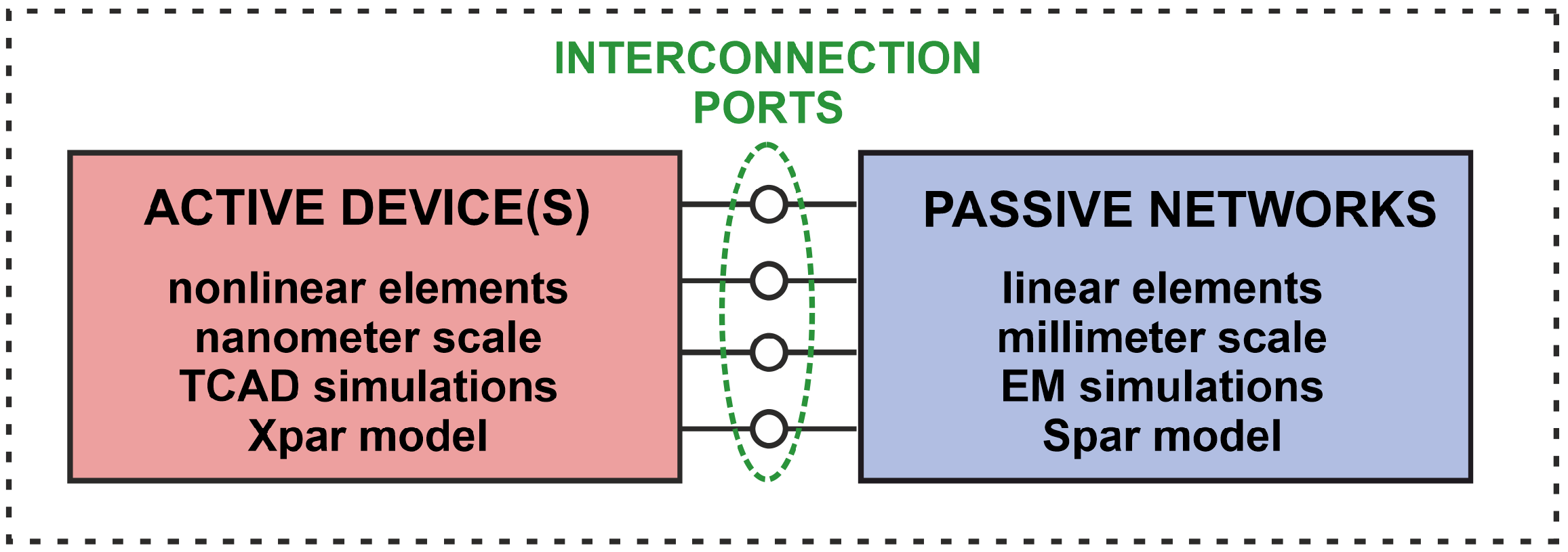
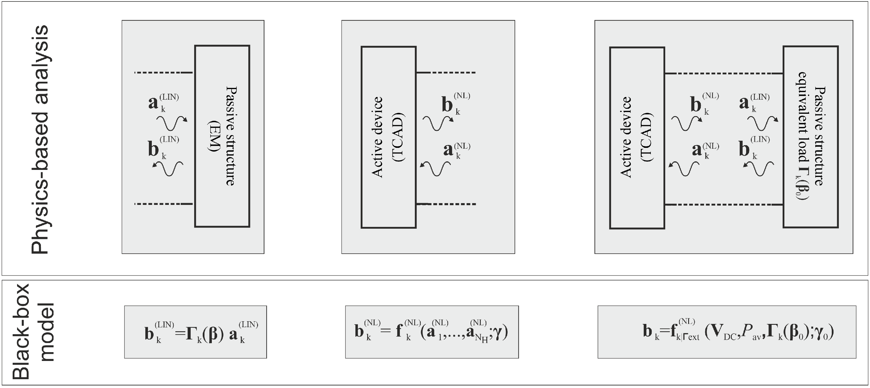
2. Block-Wise Stage Simulation through Black-Box Models

Let us consider the block-wise partition of a microwave circuit shown in Figure 1. Each block represents a physical section of the circuit, the left one encompassing the active device (including parasitics), and the right one the passive distributed structures used for matching, biasing, and coupling. We aim at modeling each block with a black-box model extracted from accurate physics-based simulations, including PIV. Such models are chosen among the ones supported for inclusion into commercial EDA tools, e.g., Keysight ADS [19] or Cadence AWR Microwave Office [20], thus allowing us to set-up a complete circuit-level simulation by connecting the black-box models by means of a set of interconnection ports. The procedure must identify (1) which black-box model is better suited for fast and accurate circuit-level analysis, and (2) how this model can be extracted from physics-based simulations.
Note that the physics-based simulation of a microwave circuit represents a true multiphysics and multiscale problem, requiring specific tools for each block as depicted in Figure 1 (thermal analysis not included). Passive structures require EM analyses, either full-3D simulations based on the finite element method (FEM, offered, e.g., by Ansys HFSS [21], Cadence AWR Analyst [22], and Comsol Multiphysics [23] commercial software), or planar-3D simulations, typically based on the methods of moments (MoM, offered, e.g., by Keysight Momentum [24], Cadence AWR Axiem [25], and Sonnet [26] commercial software), on a scale of the order of the wavelength corresponding to the operating frequency, usually spanning from hundreds of micrometers to a few millimeters in the final layout. Active devices, instead, require TCAD simulations, e.g., through the drift-diffusion model or higher-order non-stationary transport models, solved over a domain scale of a few hundredths of nanometers, with a discretization grid fine enough to include all relevant device features like doping distribution, material layers, and contact properties. Physics-based simulation may resort to general-purpose physical simulators, like Comsol Multiphysics, to more specific device TCAD commercial simulators, like Synopsys Sentaurus [27] or Silvaco Victory Device [28], or, finally, to ad hoc developed codes, like our TCAD simulator [29], which has been used for this work. MMIC thermal analysis is not included in this work, as it features manifold aspects (e.g., the coupling between the TCAD thermal model and circuit-level analysis through self-consistent electro-thermal solutions [30], or the integration with FEM-3D thermal analysis tools like Keysigth PathWave [31] or CapSym SYMMIC [32]), which would fall outside the scope of this paper, but is the object of future developments, as it is gaining an increasingly important role in a wide range of applications.
Figure 2 shows how the different blocks of Figure 1 are modeled and connected, exploiting the concept of port waves [33], which is the most natural framework for the analysis of high-frequency circuits. It is well known that EM equations are a linear (or quasi-linear) function of the external stimuli, and they are usually carried out in the frequency domain: at the k-th harmonic ω k = k ω 0 of the fundamental frequency ω 0 ( k = 1 , , N H , N H being the maximum—truncated—harmonic order included in the simulation), a given set of incident waves at all the ports a k ( LIN ) result in a set of reflected waves b k ( LIN ) at all ports and at the same frequency. The relation between these two quantities is given by the equivalent loads Γ k , which identify a black-box model of the form:
b k ( LIN ) = Γ k ( β ) a k ( LIN )
as shown in Figure 2 (left), for a simple 1-port case. In (1), Γ k is explicitly made dependent on a set of technological parameters collectively denoted by β , characterized by the nominal values β 0 and the spread δ β . For an N-port passive block, Γ k ( β ) essentially correspond to the N × N scattering matrix at ω k as a function of β .
The active device(s) in Figure 1 are modeled by means of TCAD simulations. The physical model must be solved with external periodic (or quasi-periodic) large amplitude stimuli, exciting the strong device nonlinearities, to include all the generated harmonics and the frequency mixing. These simulations require non-conventional TCAD solvers in either the time or frequency domain. Currently, only a few examples of such implementations are found in the literature: starting from the pioneering drift-diffusion simulator PISCES-HB [34], harmonic balance is exploited in our TCAD implementation that extends PISCES-HB by adding small-signal large-signal and Green’s function-based perturbation analyses [35]. Among time-domain solutions, we mention the shooting solution discussed in [36], and the Boltzmann transport equation-based simulator in [37]. The availability of Green’s functions makes our harmonic balance implementation superior for PIV analysis thanks to its numerical efficiency [38,39]. Moreover, it is better suited to extract black-box models to be incorporated into microwave EDA tools, which also employ the harmonic balance approach, and will be used hereafter in this work. Given a set of port incident waves a k ( NL ) , TCAD analysis yields the corresponding set of reflected port waves b k ( NL ) ; see Figure 2 (center). A black-box model aims at identifying a nonlinear (algebraic) vector function set f k ( NL ) (for each harmonic k = 1 , , N H , the vector function f k ( NL ) has size N, the number of device ports):
b k ( NL ) = f k ( NL ) ( a 1 ( NL ) , , a N H ( NL ) ; γ )
For each harmonic, f k ( NL ) is a function of the magnitude and phase of the incident waves at all harmonics (up to the truncation order N H ), and of a set of physical device parameters γ (e.g., the doping profile or the gate length) with nominal values γ 0 and technological spread δ γ . As anticipated, the model in (2) does not include any temperature-dependent effect, as temperature in the TCAD simulations is kept constant at 300 K.
Identifying the nonlinear functions f k ( NL ) would be a true challenge: TCAD simulations should be repeated with different amplitudes and phases of all the incident waves to collect all the reflected waves. Interpolating a model over such a huge amount of data seems impractical. To downsize the problem, the device ports are terminated with a fixed embedding circuit, composed of prescribed harmonic loads characterized by the scattering matrix Γ k , ext , a given set of bias sources V DC , and an input generator with swept available power P av (we assume here a single tone excitation for the sake of simplicity). With such a constraint, model (2) becomes
b k ( NL ) = f k | Γ ext ( NL ) ( V DC , P av , Γ ext ; γ )
The most natural choice is
Γ k , ext = Γ k ( β 0 )
i.e., to embed the device with the equivalent loads presented by the passive structure with nominal parameters at each harmonic k. The model identification requires now the self-consistent solution of the two connected blocks, Figure 2 (right), corresponding to a TCAD mixed-mode analysis, whereby the physical device model is solved self-consistently with the circuit equations for the embedding structure (including bias, power source, and external loads). Harmonic balance enforces the port wave continuity:
a k ( LIN ) = b k ( NL ) b k ( LIN ) = a k ( NL )
yielding the solution a k 0 ( NL ) , a k 0 ( LIN ) , b k 0 ( NL ) , b k 0 ( LIN ) , where the subscript “0” refers to the system at the nominal operating condition and nominal technological parameters, i.e., β = β 0 and γ = γ 0 .
We now discuss the model dependency on technological variations, i.e., γ = γ 0 + δ γ and/or β = β 0 + δ β . Variations δ β of β in the passive block correspond to variations δ Γ k of the equivalent load Γ k at each harmonic. Since δ β is not a deterministic quantity that can be set a priori, but rather a stochastic term following a prescribed statistical distribution, we must regard δ Γ k to be a free variation from the nominal load, with amplitude and phase continuously varying in a domain around Γ k ( β 0 ) , as illustrated in Figure 3.
From the active device standpoint, δ Γ k corresponds to equivalent load variations, effectively load-pulling the device around the nominal load. Therefore, to include PIV, the nonlinear block model must be either a global model as a function of Γ k (e.g., akin to (2)), or at least include local load-pull capability. Equivalently, it must account for the wave port variations δ a k ( NL ) , δ b k ( NL ) around their nominal values due to the load variations shown in Figure 3, as depicted in Figure 4 (left). Furthermore, technological variations δ γ in the active device induce further port wave variations, hence contributing to load-pulling the device, as detailed in Section 4.
For port wave continuity at the interconnecting ports, linear blocks also undergo port wave variations δ a k ( LIN ) , δ b k ( LIN ) , as shown in Figure 4 (left). We conclude that, with respect to the model with nominal parameters, a PIV-dependent model must include the dependency on both technological variations (endogenous, i.e., resulting from internal variations of each block) and port wave variations (exogenous, i.e., resulting from variations of the embedding blocks).
To model technological variations, two main approaches can be used:
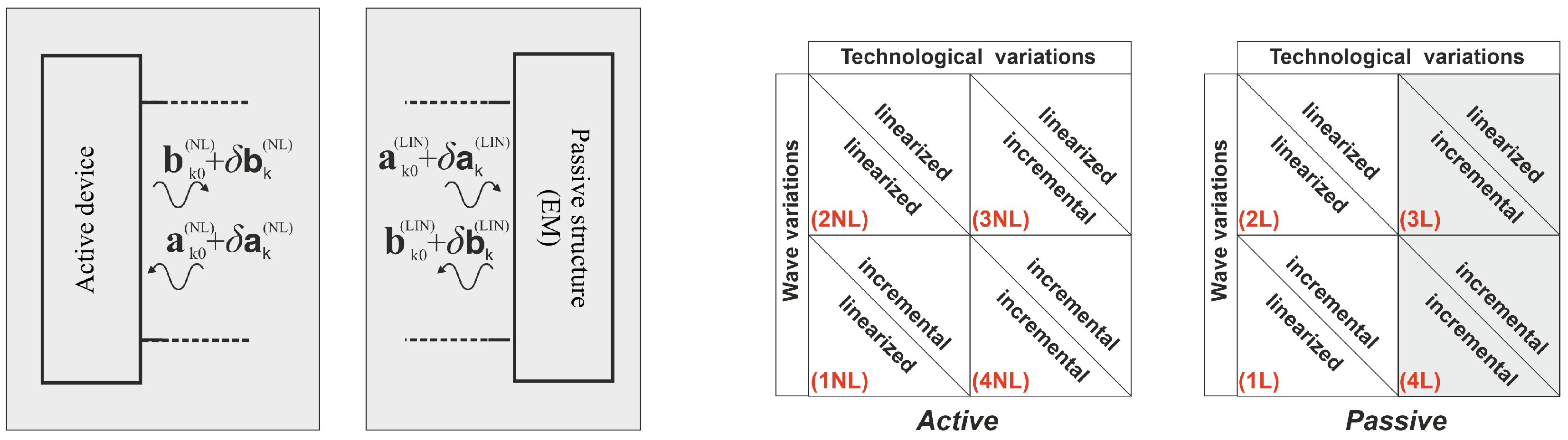
  • incremental approach: repeated physical simulations are carried out, varying each technological parameter β i and γ i on a set of prescribed values β i l and γ i l , respectively. A family of models Γ k ( β i l ) and f k ( NL ) ( a 1 ( NL ) , , a N H ( NL ) , γ i l ) are extracted and fed to the EDA tool, where interpolation among these models allows for statistical analysis or optimization with continuously varying β and γ ;
  • linearized approach: when variations are small, physical simulations are used to assess the sensitivity of the given nominal model to each of the i-th parameter variations
    S k ( β i ) = Γ k β i β i = β 0 , i ; S k ( γ i ) = f k | Γ ext ( NL ) γ i γ i = γ 0 , i
The same two approaches also apply to wave variations:
  • incremental approach: repeated physical simulations with varying incident waves a k (magnitude and phase) yield a set of reflected waves and a family of models. Interpolation allows us to incorporate them into EDA tools;
  • linearized approach: the models must be linearized as a function of the incident waves a k .
Combining the above approaches, we obtain four possible cases, as shown in Figure 4 (right). Actually, since the passive network is itself linear as a function of the port waves, the linearized and incremental models would coincide, and thus we neglect cases (3L) and (4L). For the active device, instead, all four cases are possible. Note that, since technological variations are static, wave variations occur at the same fundamental frequencies as the nominal operating condition.

3. Passive Block Black-Box Models

For the passive blocks, we address separately the two cases (1L) and (2L) of Figure 4.

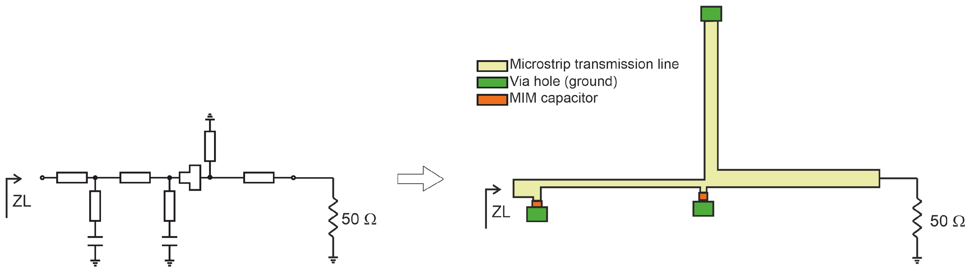
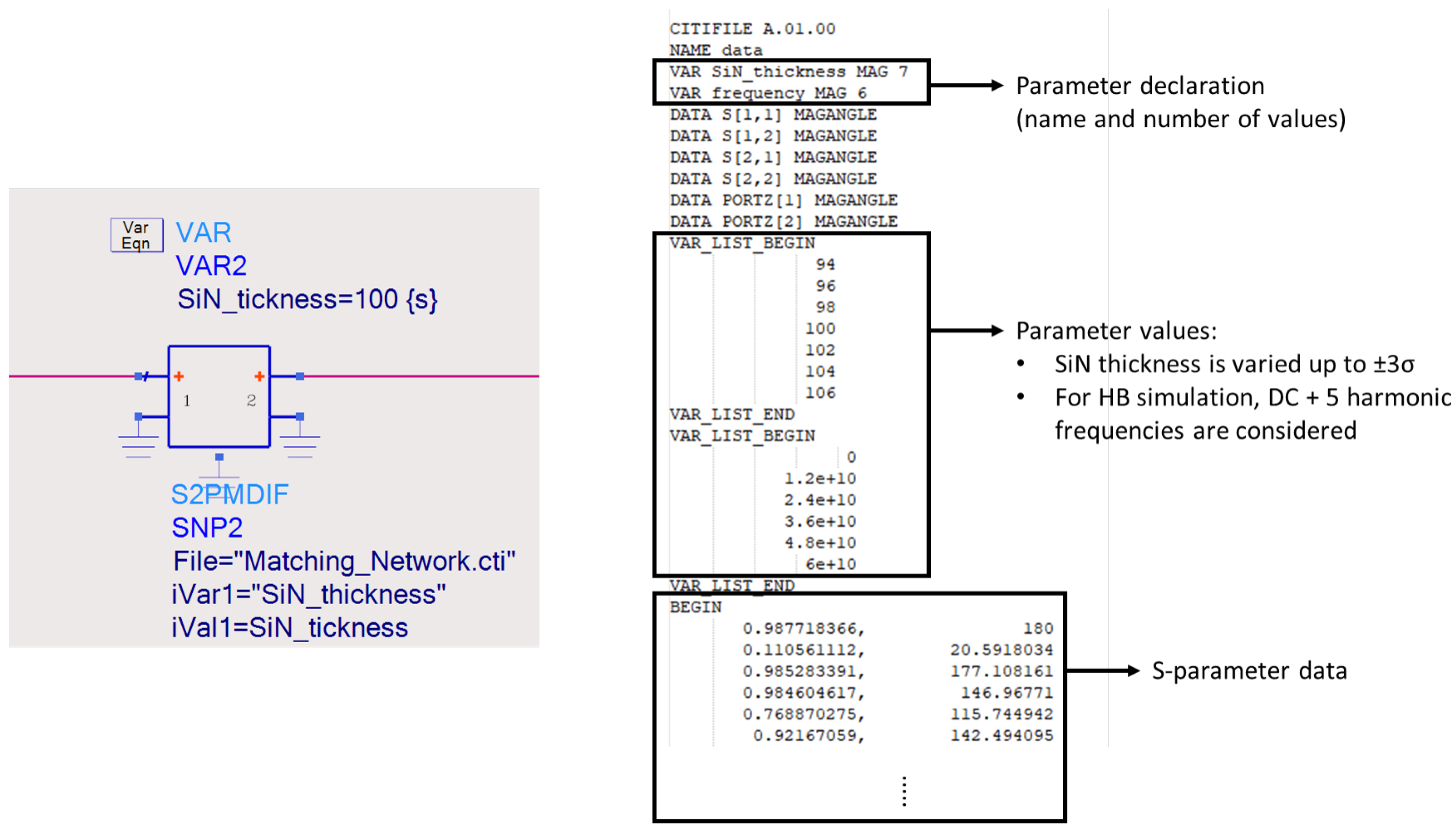
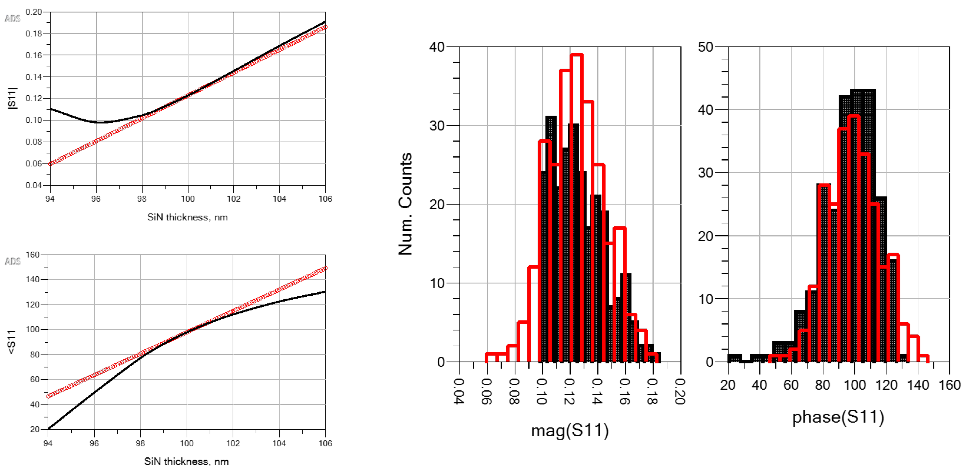
3.1. Case (1L): Look-Up Table MDIF File

In case (1L) the model is not linearized in terms of technology variations. To clarify the procedure, we consider first the dependency on a single parameter β : repeated EM simulations are carried out varying β over a prescribed range with a set of samples β l , l = 1 , , N β . The range and the number of samples must be chosen according to the technology used for the circuit development. The resulting values Γ k ( β l ) can be collected in terms of a look-up table as a function of the parameter β , for further inclusion in EDA circuit simulations. To clarify the procedure, we take as an example the output matching network (OMN) of a power amplifier (PA) designed at 12 GHz and implemented in MMIC GaAs technology for X-band applications [40,41]. The OMN synthesizes a load Z L = 43 + j 10 Ω at the fundamental frequency, shunting up to the third harmonic and minimizing the impedance at higher harmonics. For the design, we adopt a proprietary MMIC foundry PDK exploiting two gold layers (1 μm and 2 μm thick) for micro-strip transmission lines and a 100-nm-thick SiN insulating layer for MIM capacitors (resulting in about 600 pF/mm 2 capacitance per unit area). A preliminary layout of the OMN with nominal technological parameters is shown in Figure 5.
Let us address the OMN PIV, focusing in particular on the variability due to the uncertainty of the dielectric layer thickness t SiN in MIM capacitors. According to the foundry specifications, t SiN is subject to variations estimated about ± 2 % around the nominal value of 100 nm. Hence, in Monte Carlo analysis, the PDK suggests to randomly distribute t SiN according to a Gaussian distribution with σ = 2 nm standard deviation, corresponding to the 2% foundry uncertainty. To sample such a distribution, we run EM simulations with t SiN equal to the nominal value and for other 6 values, corresponding to a variation of ± σ , ± 2 σ , ± 3 σ . Variations of t SiN are considered to be fully correlated over a correlation length comparable with the OMN dimensions, i.e., the variations are not local but global. If this hypothesis is relaxed, variations undergo partial compensation over a scale greater than the correlation length effectively reducing the overall effect of t SiN variations. Hence, the global variation case can be regarded as a worst-case bound for PIV.
EM simulations were carried out within ADS, through the full-wave planar-3D Momentum simulation engine. The EM simulation results are collected into a look-up table model: we have used the ADS S2PMDIF component shown in Figure 6 [42]. It is essentially a 2-port scattering parameter model that allows for parametrization over an external quantity via the measurement data interchange format (MDIF) standard. The MDIF model consists of an ADS citifile collecting the EM simulated S-parameters up to the fifth-harmonic frequency as a function of t SiN . As an example, Figure 7 (left) shows the OMN S 11 for each harmonic and the sampled values of t SiN , highlighting their range of variation. With continuously varying the oxide thickness from 92 nm to 108 nm, ADS interpolates/extrapolates the citifile data using polynomials or splines, as shown by the red line in Figure 7 (right). As expected, the interpolation capability of the algorithm is excellent, while attention must be paid when trying to extrapolate. Notice that the circuit-level analysis is considerably more efficient from the numerical standpoint: the EM simulation took approximately 15 min for each dielectric layer thickness, while the circuit-level simulation with more than 150 t SiN values that generates the data shown in Figure 7 (right) is almost instantaneous. Since the final passive circuit-level model is lookup-table-based, the proposed method is very general and can be extracted from more accurate full-3D EM simulators external to ADS. Of course, if multiple parameters are simultaneously considered, the space over which the model must be sampled becomes multidimensional and the interpolation of the look-up table data requires a careful choice of the sampling points.

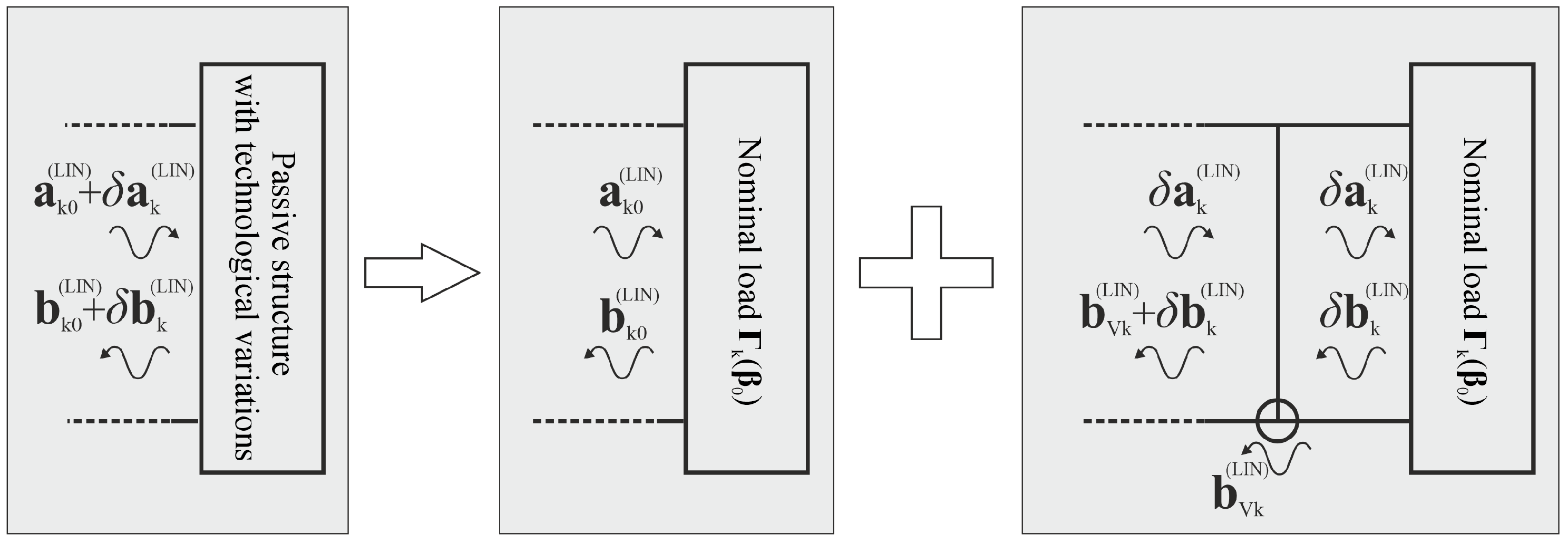
3.2. Case (2L): Equivalent PIV Generators

For case (2L) in Figure 4, the model must be linearized as a function of β :
Γ k β Γ k β 0 + i = 1 N β S k ( β i ) δ β i = Γ k β 0 + δ Γ k
where S k ( β i ) are the model sensitivities defined in (6). At first order:
b k 0 ( LIN ) + δ b k ( LIN ) = Γ k β 0 + δ Γ k a k 0 ( LIN ) + δ a k ( LIN ) δ b k ( LIN ) Γ k β 0 δ a k ( LIN ) + δ Γ k a k 0 ( LIN )
i.e.,
δ b k ( LIN ) Γ k β 0 δ a k ( LIN ) + b V k ( LIN )
where b V k ( LIN ) = δ Γ k a k 0 ( LIN ) acts as an equivalent impressed wave generator [43] proportional to the technological variations, as shown in Figure 8.
The model is entirely identified by the parametric sensitivity, which can be extracted numerically with only two EM simulations, i.e., one with the nominal parameter value, and a second one with a small perturbation. The simulation time for the model extraction is therefore reduced with respect to the incremental case. EM solvers allowing for numerically efficient ways to calculate the sensitivities, e.g., through a Green’s function (GF) approach similar to the one used in the active device physical simulations, would further reduce the model extraction time. GFs would also allow us to efficiently take into account local variations of the dielectric thickness but, as already explained, we take global variations as a worst-case bound.
The model of Figure 8 is implemented into ADS with ad hoc equivalent generators and compared with the look-up-table model of case (1L). Considering again the OMN example of the previous section with t SiN varying in the interval [94, 106] nm, Figure 9 (left) shows that the linearized model cannot predict the significant nonlinearity of the S 11 magnitude for t SiN < 98 nm, while the phase has overall nonlinear behavior. The effect of nonlinearity is especially evident in the statistical analysis required for PIV. The Monte Carlo OMN simulations, with t SiN taking random values with a Gaussian distribution with 2 nm variance, is shown in Figure 9 (right). The distribution of S 11 magnitude and phase obtained from the MDIF incremental model shows a pronounced skew, whereas the linearized model predicts instead Gaussian symmetric behavior.
The result shown is not unusual. Even if in a mature technology parameter variations are expected to be small with respect to their nominal values, the sensitivity of the distributed matching network to the transmission line length or width can be very important, e.g., at the resonance frequencies. We remark that the nonsymmetric feature of the statistical distribution is especially important to correctly identify the corners for yield analysis. Since the ADS simulation time is practically the same for both the incremental and linearized analysis, we conclude that the obtained accuracy and time saving is not sufficient to justify the linearized approach, while the look-up-table models (case (1L)) are a better compromise between simulation speed and accuracy.

4. Active Device Black-Box Model

Extracting a black-box model for the active device PIV is the most challenging part, since active device black-box models are already challenging per se, even without considering variability.
In principle, for the active block all of the four cases (1NL)–(4NL) of Figure 4 must be considered. Cases (3NL)–(4NL), however, require load-pull physical simulations with varying loads. The number of simulations required is calculated sampling the multi-dimensional space made of the real and imaginary parts of Γ k plus the technological parameters γ . The only way to exploit this amount of data in EDA simulations would be through a generalized MDIF (GMDIF), a data format specifically developed for accessing/saving multidimensional data (multiple independent vs. dependent variables) external to the circuit simulator, e.g., from measurements or independent physical simulations, basically extending the MDIF format used in Section 3, which was limited to linear blocks. The GMDIF format can be used to collect data representing the device in nonlinear conditions, e.g., the harmonic components of the currents, voltages, or port waves as a function of input power, γ , and load. Although a multidimensional interpolation over the parameter domain is in principle possible, such a model turns out to be a too demanding task. Furthermore, the model accuracy may also be poor. Therefore cases (3NL) and (4NL) will be not discussed any further.
In this work we propose to circumvent the multidimensional interpolation issue by using the Xpar model [18], a black-box model where the device is linearized around a nominal operating condition, corresponding to a prescribed port load. As such, X-parameters seem to be the ideal choice to address cases (1NL) and (2NL).
The Xpar model expresses the reflected waves at the device ports as a linearized function of the incident waves, therefore extending the concept of S-parameters to the non-linear large-signal (LS) regime. A power source, e.g., a single tone generator, drives the device in a nonlinear LS operating condition with ports terminated on a fixed reference load Γ ext , typically 50 Ω . To fix the ideas, we consider the single-tone injection in port 1 at the first harmonic. Small-amplitude incident waves are added to each device port and each harmonic (with the exception of the same port and the same frequency of the LS excitation) to perturb the LS working point. According to the multiharmonic linearization around the LS working point [44], the reflected waves b k ( NL ) at the k-th harmonic can be expressed by the LS value plus a superposition of the small incident waves a l ( NL ) at the other harmonics:
b k ( NL ) = X k F ( | a 11 | , V DC , γ ) + l = 1 , N H X k l S ( | a 11 | , V DC , γ ) P k l a l ( NL ) + l = 1 , N H X k l T ( | a 11 | , V DC , γ ) P k l a l ( NL ) *
The Xpar functions X F , X S , and X T fully identify the model, depending on the DC bias voltages and the input large signal incident wave at fundamental frequency | a 11 | or, equivalently, on the available power P a v if the source impedance is chosen to be equal to the normalization impedance. In order to include PIV, the Xpar model is made dependent on the active device technological parameters γ . Equation (9) can be regarded as a particular way of linearizing (3) around the nominal LS working point with reference loads Γ ext : as discussed in [44], X F relates to the AM-AM/AM-PM curves with a perfectly matched output impedance (typically 50 Ω ), while X S and X T are sensitivity terms accounting for the device response to a (small) load mismatch, as required in the PIV analysis (see Figure 3). Sampling the Xpar model over a prescribed input power interval, e.g., driving the device from back-off to compression, we generate a look-up-table model (black-box model) suited for circuit-level analysis. Here we adopt the proprietary ADS .xnp file format and the corresponding Xpar schematic component [19].
The multiharmonic linearization around the LS working point, on which Xpars are based, is a problem addressed more generally by the sideband conversion analysis, where the small perturbation is imposed at a frequency displaced with respect to the LS harmonic by the sideband frequency [45]; see Figure 10. Xpars can be regarded as a special case, when the perturbation occurs at the same LS harmonics, i.e., with null sideband frequency; in fact, a one-to-one relationship exists between the two representations [44]. According to the sideband analysis, a sideband conversion matrix (SCM) describes frequency conversion among sidebands in terms of a matrix product, i.e., a linear superposition [45]. Sideband conversion analysis was introduced within the framework of TCAD simulations in [35], and was later extended to device variability and sensitivity analyses [38,39,46] and to assist the PIV-aware microwave circuit design [47,48,49]. In our in-house TCAD simulator, the admittance SCM Y is calculated with short-circuited device ports and converted into the scattering SCM S by
S = I + Z 0 Y 1 I Z 0 Y
where Z 0 is a block diagonal matrix with entries equal to the reference port impedance Z 0 for each harmonic and I is the identity matrix [40].
For implementation reasons, the SCM evaluated into TCAD tools is defined with reference to a bilateral spectrum, so that the harmonic index runs from N H to N H . Furthermore, the frequency offset taken into account is positive, so that upper sidebands only are used. On the contrary, as can be seen from (9), Xpars differentiate the contributions from the upper and lower sidebands of each harmonic using both the incident waves a l ( NL ) and their complex conjugates ( a l ( NL ) ) * . However, spectral symmetry implies that the upper sideband of a negative frequency harmonic p < 0 corresponds to the lower sideband of harmonic p for the unilateral spectrum. Therefore, as shown in Figure 10, for each ( k , l > 0 ), S can be converted into the S k l and T k l Xpars as follows:
  • X k l S is identified with the ( k , l ) elements of S
  • X k l T is identified with the ( k , l ) elements of S

4.1. Case (1NL): Look-Up Table X-Parameters

To account for the dependency of the Xpars on process variability, TCAD simulations of the active device are carried out with technological parameters γ varying over a prescribed interval with N γ samples, and a look-up-table-based Xpar model interpolates among available data to make the Xpar model depend continuously on γ . To demonstrate the procedure, we consider the design of a power amplifier stage exploiting an FET GaAs MESFET as the active device [48]. The PA is designed for the tuned load deep class AB operation (10% I DSS ) at 12 GHz, with optimum load Z L , opt = ( 43 + j 10 ) Ω at the fundamental frequency and shorted harmonics. With this loading condition, we investigate the FET behavior with varying channel doping ( γ = N D ) in the interval ± 10 % around the nominal value N D = 2 × 10 17 cm 3 [40]. The aim is to extract a dependable Xpar device model to be used in the final design of the PA, describing the doping dependence and the effect of possible deviations from the nominal value of the optimum load.
To extract the Xpar model, TCAD simulations have been carried out with three doping values (nominal, and ± 10 % ) and the device ports terminated on matched loads (50 Ω at all ports and all harmonics). Xpars were extracted for each doping value using the S SCM as explained above, and stored in a unique ADS .xnp file which, being itself a particular form of a GMDIF, allows for the interpolation of the Xpars over any independent variable. To make the interpolation simpler, we inserted an additional, fictitious port in the Xpar model; the extra port is isolated from the other ones (Xpars are padded with zeros to avoid interfering with the other active ports) and its port voltage, set to a desired doping value, only allows for the interpolation over doping in the Xpar file (see Figure 11).
TCAD simulations have then been repeated with ideal tuners implementing the optimum load (Figure 12). These simulations will be used for the Xpar model validation. Doping variations highly affect the device nonlinear operation. In fact, the drain current increases with higher doping concerning both the DC bias and the harmonic amplitudes, giving rise to different behaviors at varying input power. At a lower input drive, Figure 12 left, the device biased in class AB exhibits the transition from a “class-A-like” behavior to a “class-B-like” case, with a significant clipping of the drain waveform. Such transition is significantly impacted by doping: the lower is the doping, the more the device is pushed towards the class-B-like behavior, due to the reduction of the bias current, while the opposite is true when doping is increased. Even in harsh compression, Figure 12 right, doping affects significantly the device operating condition. In particular, the knee voltage is lower with higher doping, resulting in a larger voltage swing and output power.
Turning to the Xpar model validation, simulations have been carried out within ADS exploiting the active device Xpar model loaded with ideal tuners implementing the optimum load. Note that such load differs from the one used for the Xpar model extraction (50 Ω ). Nonetheless, Xpars easily accommodate both for the load mismatch and doping variations, both in back-off and compression, as shown by the dynamic load lines (DLLs) in Figure 13, where the drain current is plotted against both the drain voltage and the gate voltage. The accuracy is always remarkable, up to a doping variation of ± 10 % and with input power ranging from back-off to compression: even doping variations of ± 5 %, not used for the Xpar model extraction, are correctly modeled, showing the accuracy of the ADS interpolation capability within the GMDIF data file. The accuracy of the Xpar model is further verified by the gate current DLL (Figure 14), showing the gate current as a function of the gate voltage at the input port. Such DLLs demonstrate the dependence of the input gate nonlinear capacitance on doping, and are extremely valuable in the design of a power amplifier, since they predict the input mismatch. Even in this case the accuracy is extremely satisfying up to a ± 10 % doping variation.
Notice that the simulation time for the TCAD analysis on a 25 values input power sweep and 10 harmonics is around 20 h for each doping value, while the Xpar simulations within ADS allow for the accuracy shown in Figure 11 in just a few seconds of simulation time.

4.2. Case (2NL): X-Parameters with Equivalent PIV Generators

Linearizing (3) with respect to the physical parameters γ i we have:
b k ( NL ) = f k | Γ ext ( NL ) ( V DC , P av , Γ ext , γ 0 ) + i = 1 N γ S k ( γ i ) δ γ i
where we have used the sensitivity defined in (6). As in the (2L) case, equivalent wave impressed generators b V k ( NL ) can be added to the nominal device ports to describe parametric variations; see Figure 15 (left):
b k ( NL ) = b k 0 ( NL ) + i = 1 N γ S k ( γ i ) δ γ i = b k 0 ( NL ) + b V k ( NL )
The equivalent PIV generators can be calculated by TCAD concurrently with the device S SCM [29] by means of a Green’s function approach: localized technological variations inside the device are transferred by the GFs to equivalent port wave variations. The GF approach greatly reduces the computational cost of TCAD variability analysis, since the relevant propagation quantities must be calculated only once for the nominal parameters γ 0 , thus avoiding repeated simulations. Furthermore, the same analysis allows us to calculate the linearized electrical model through the Xpars, also requiring the same S SCM [29]. The resulting model is therefore a doubly linear model, both in terms of port waves and in terms of parameter variations. The method is applied to the same GaAs FET used for case (1NL). The schematic in Figure 15 (right) shows the implementation in ADS: the Xpar model is now required only for the nominal doping and reduced to a 4-port (the extra DOPING port is eliminated), while short circuit current generators are used at the input and output DC and RF ports to generate the PIV equivalent waves. The equivalent generators extracted from TCAD are stored in dataset files for each harmonic, and accessed via the data access component in ADS.
As an example of the obtained results, Figure 16 shows the model accuracy on the same PA on class AB optimum load as in previous Section 4.1. The agreement is very good up to ± 5 % doping variations, but is less satisfying at ± 10 % doping variations. The accuracy diminishes especially at the lower doping values and lower input drive, where the operating condition of the device has a very strong dependency on doping. Although the linearized model validity is restricted to a more limited interval with respect to the incremental Xpar model (case (1NL)), it may be still sufficient to describe most of the process-induced doping variations in a mature technology. This is not the case for extremely downsized CMOS or FinFET devices, featuring gate lengths below 20 nm, where the doubly linear model based on linearization may not be sufficient to describe large statistical fluctuations. However, it may be appealing for three applications:
  • Case (2NL) provides a simple way to couple experimental Xpar characterization on a limited set of sample (“nominal”) devices with the equivalent PIV generators extracted in an independent way, i.e., through physical simulations. This would avoid the time-consuming and costly statistical characterization campaigns on a given technology, a procedure well beyond the typical laboratory capabilities usually available to microwave designers.
  • Green’s functions allow for a dramatic reduction of the model extraction time when we address concurrent multiple variations of technological parameters; in fact, GFs must be calculated just once with the nominal parameter values, and equivalent port generators are readily calculated for all variations. Hence, case (2NL) avoiding the multidimensional interpolation of look-up-table data, may turn out to be more robust from the numerical standpoint. However, linearization also implies that multiple uncorrelated parameters will also induce fully uncorrelated equivalent PIV generators, a result that has been proven wrong in some aggressively downscaled technologies [50].
  • Green’s functions allow us to easily address the effect of local fluctuations [38]. Although in this paper we restricted the analysis to global variations, local variations (also statistical in nature) are quite usual in silicon technologies, e.g., for random doping fluctuations [50]. Nonetheless, the efficient calculation of GFs in TCAD is not at all conventional. Up to now, GF-based variability analysis within the harmonic balance approach (i.e., for nonlinear large signal applications) is unique to our in-house software [29], and it is not available in any commercial simulator (indeed Synopsys Sentaurus [27] does implement a GF-based variability analysis, but limited to the DC case only).
As a conclusion, a careful choice between case (1NL) and (2NL) must be considered for each specific technology. For a limited number of parameters, approach (1NL) reveals to be preferable for its superior accuracy.

5. Conclusions

We have addressed the problem of incorporating process-induced variability in the design of MMICs for the next generation of communications systems, where fabrication tolerances and nanometric device features will significantly impact the circuit performance. Statistical analysis of such variations requires accurate modeling strategies due to their ubiquitous presence in all the physical sections of the integrated circuit. In particular, we have shown a flexible procedure to extract black-box models from physical simulations to be readily integrated into commercial EDA tools for MMIC design, retaining a direct link to the fabrication process of both the passive and active circuit components, hence allowing for a PIV aware design.

Author Contributions

Conceptualization, methodology, and writing—review and editing, all authors; investigation, funding acquisition and writing—original draft preparation, S.D.G. All authors have read and agreed to the published version of the manuscript.

Funding

This work has been supported by the Italian Ministero dell’Istruzione dell’Universit`a e della Ricerca (MIUR) under the PRIN 2017 Project “Empowering GaN-on-SiC and GaNon-Si technologies for the next challenging millimeter-wave applications (GANAPP)”.

Conflicts of Interest

The authors declare no conflict of interest.

References

  1. Lee, H.J.; Callender, S.; Rami, S.; Shin, W.; Yu, Q.; Marulanda, J.M. Intel 22nm Low-Power FinFET (22FFL) Process Technology for 5G and Beyond. In Proceedings of the 2020 IEEE Custom Integrated Circuits Conference (CICC), Newport Beach, CA, USA, 22–25 March 2020. [Google Scholar] [CrossRef]
  2. Lin, H.C.; Chou, T.; Chung, C.C.; Tsen, C.J.; Huang, B.W.; Liu, C.W. RF Performance of Stacked Si Nanosheet nFETs. IEEE Trans. Electron Devices 2021, 68, 5277–5283. [Google Scholar] [CrossRef]
  3. Wang, Z.; Wang, H.; Heydari, P. CMOS Power-Amplifier Design Perspectives for 6G Wireless Communications. In Proceedings of the 2021 IEEE International Midwest Symposium on Circuits and Systems (MWSCAS), East Lansing, MI, USA, 8–11 August 2021. [Google Scholar] [CrossRef]
  4. Raskin, J.P. FinFET versus UTBB SOI—A RF perspective. In Proceedings of the 2015 45th European Solid State Device Research Conference (ESSDERC), Graz, Austria, 14–18 September 2015. [Google Scholar] [CrossRef]
  5. Collaert, N.; Alian, A.; Banerjee, A.; Chauhan, V.; ElKashlan, R.Y.; Hsu, B.; Ingels, M.; Khaled, A.; Kodandarama, K.V.; Kunert, B.; et al. From 5G to 6G: Will compound semiconductors make the difference? In Proceedings of the 2020 IEEE 15th International Conference on Solid-State & Integrated Circuit Technology (ICSICT), Kunming, China, 3–6 November 2020. [Google Scholar] [CrossRef]
  6. Poluri, N.; DeSouza, M.M.; Venkatesan, N.; Fay, P. Modelling Challenges for Enabling High Performance Amplifiers in 5G/6G Applications. In Proceedings of the 2021 28th International Conference on Mixed Design of Integrated Circuits and System, Lodz, Poland, 24–26 June 2021. [Google Scholar] [CrossRef]
  7. White Paper on RF Enabling 6G—Opportunities And Challenges From Technology To Spectrum; Technical Report; University of Oulu: Oulu, Finland, 2021; Available online: https://www.keysight.com/us/en/assets/7121-1085/article-reprints/RF-Enabling-6G-Opportunities-and-Challenges-from-Technology-to-Spectrum.pdf (accessed on 30 January 2022).
  8. Camarchia, V.; Donati Guerrieri, S.; Ghione, G.; Pirola, M.; Quaglia, R.; Rubio, J.J.M.; Loran, B.; Palomba, F.; Sivverini, G. A K-band GaAs MMIC Doherty power amplifier for point-to-point microwave backhaul applications. In Proceedings of the 2014 International Workshop on Integrated Nonlinear Microwave and Millimetre-wave Circuits (INMMiC), Leuven, Belgium, 2–4 April 2014. [Google Scholar] [CrossRef] [Green Version]
  9. Mao, S.; Zhang, W.; Yao, Y.; Yu, X.; Tao, H.; Guo, F.; Ren, C.; Chen, T.; Zhang, B.; Xu, R.; et al. A Yield-Improvement Method for Millimeter-Wave GaN MMIC Power Amplifier Design Based on Load—Pull Analysis. IEEE Trans. Microw. Theory Tech. 2021, 69, 3883–3895. [Google Scholar] [CrossRef]
  10. Bonani, F.; Camarchia, V.; Cappelluti, F.; Donati Guerrieri, S.; Ghione, G.; Pirola, M. When self-consistency makes a difference. IEEE Microw. Mag. 2008, 9, 81–89. [Google Scholar] [CrossRef] [Green Version]
  11. Ramella, C.; Pirola, M.; Reale, A.; Ramundo, M.; Colantonio, P.; Maur, M.A.D.; Camarchia, V.; Piacibello, A.; Giofrè, R. Thermal-aware GaN/Si MMIC design for space applications. In Proceedings of the IEEE International Conference on Microwaves, Communications, Antennas, and Electronic Systems (IEEE COMCAS 2019), Tel-Aviv, Israel, 4–6 November 2019; pp. 1–6. [Google Scholar] [CrossRef] [Green Version]
  12. Wen, Z.; Mao, S.; Wu, Y.; Xu, R.; Yan, B.; Xu, Y. A Quasi-Physical Large-Signal Statistical Model for 0.15 μm AlGaN/GaN HEMTs Process. In Proceedings of the 2019 IEEE MTT-S International Microwave Symposium (IMS), Boston, MA, USA, 2–7 June 2019. [Google Scholar] [CrossRef]
  13. Williams, S.; Varahramyan, K. A new TCAD-based statistical methodology for the optimization and sensitivity analysis of semiconductor technologies. IEEE Trans. Semicond. Manuf. 2000, 13, 208–218. [Google Scholar] [CrossRef]
  14. Chordia, A.; Hemaram, S.; Tripathi, J.N. A Swarm Intelligence based Automated Framework for Variability Analysis. In Proceedings of the 2020 IEEE MTT-S Latin America Microwave Conference (LAMC 2020), Cali, Colombia, 26–28 May 2021. [Google Scholar] [CrossRef]
  15. Geng, M.; Zhu, Z.; Cai, J. Small-Signal Behavioral Model for GaN HEMTs based on Long-Short Term Memory Networks. In Proceedings of the 2021 IEEE MTT-S International Wireless Symposium (IWS), Nanjing, China, 23–26 May 2021. [Google Scholar] [CrossRef]
  16. Hu, W.; Luo, H.; Yan, X.; Guo, Y.X. An Accurate Neural Network-Based Consistent Gate Charge Model for GaN HEMTs by Refining Intrinsic Capacitances. IEEE Trans. Microw. Theory Tech. 2021, 69, 3208–3218. [Google Scholar] [CrossRef]
  17. Orengo, G.; Colantonio, P.; Giannini, F.; Pirola, M.; Camarchia, V.; Donati Guerrieri, S. Advanced Neural Network Techniques for GaN-HEMT Dynamic Behavior Characterization. In Proceedings of the 2006 European Microwave Integrated Circuits Conference, Manchester, UK, 10–13 September 2006. [Google Scholar] [CrossRef]
  18. Root, D.; Verspecht, J.; Horn, J.; Marcu, M. X-Parameters: Characterization, Modeling, and Design of Nonlinear RF and Microwave Components; Cambridge University Press: Cambridge, UK, 2013. [Google Scholar]
  19. Keysight ADS. Available online: https://www.keysight.com/zz/en/products/software/pathwave-design-software/pathwave-advanced-design-system.html (accessed on 30 January 2022).
  20. Cadence AWR Microwave Office. Available online: https://www.awr.com/awr-software/products/microwave-office (accessed on 30 January 2022).
  21. Ansys HFSS. Available online: https://www.ansys.com/it-it/products/electronics/ansys-hfss (accessed on 30 January 2022).
  22. Cadence AWR Analyst. Available online: https://www.awr.com/awr-software/products/analyst (accessed on 30 January 2022).
  23. Comsol Multiphysics. Available online: https://www.comsol.com/products (accessed on 30 January 2022).
  24. Keysight Momentum. Available online: https://www.keysight.com/it/en/product/W3031E/pathwave-momentum.html (accessed on 30 January 2022).
  25. Cadence AWR Axiem. Available online: https://www.cadence.com/en_US/home/tools/system-analysis/rf-microwave-design/awr-axiem-analysis.html (accessed on 30 January 2022).
  26. Sonnet. Available online: https://www.sonnetsoftware.com/products/sonnet-suites/ (accessed on 30 January 2022).
  27. Synopsys Sentaurus. Available online: https://www.synopsys.com/silicon/tcad/device-simulation/sentaurus-device.html (accessed on 30 January 2022).
  28. Silvaco Victory Device. Available online: https://silvaco.com/tcad/victory-device-3d/ (accessed on 30 January 2022).
  29. Donati Guerrieri, S.; Pirola, M.; Bonani, F. Concurrent Efficient Evaluation of Small-Change Parameters and Green’s Functions for TCAD Device Noise and Variability Analysis. IEEE Trans. Electron Devices 2017, 64, 1269–1275. [Google Scholar] [CrossRef]
  30. Catoggio, E.; Donati Guerrieri, S.; Bonani, F. Efficient TCAD Thermal Analysis of Semiconductor Devices. IEEE Trans. Electron Devices 2021, 68, 5462–5468. [Google Scholar] [CrossRef]
  31. Keysight PathWave Thermal Design. Available online: https://www.keysight.com/it/en/products/software/pathwave-design-software/pathwave-thermal-design-software.html (accessed on 30 January 2022).
  32. Capesym Symmic. Available online: https://www.capesym.com/symmic.html (accessed on 30 January 2022).
  33. Ghione, G.; Pirola, M. Microwave Electronics; Cambridge University Press: Cambridge, UK, 2019. [Google Scholar]
  34. Dutton, R.; Troyanovsky, B.; Yu, Z.; Arnborg, T.; Rotella, F.; Ma, G.; Sato-Iwanaga, J. Device simulation for RF applications. In Proceedings of the International Electron Devices Meeting, IEDM Technical Digest, Washington, DC, USA, 10 December 1997; pp. 301–304. [Google Scholar] [CrossRef]
  35. Bonani, F.; Donati Guerrieri, S.; Ghione, G.; Pirola, M. A TCAD approach to the physics-based modeling of frequency conversion and noise in semiconductor devices under large-signal forced operation. IEEE Trans. Electron Devices 2001, 48, 966–977. [Google Scholar] [CrossRef]
  36. Bertazzi, F.; Bonani, F.; Donati Guerrieri, S.; Ghione, G. Large-signal device simulation in time- and frequency-domain: A comparison. COMPEL—Int. J. Comput. Math. Electr. Electron. Eng. 2008, 27, 1319–1325. [Google Scholar] [CrossRef] [Green Version]
  37. Guerra, D.; Saraniti, M.; Ferry, D.K.; Goodnick, S.M. X-parameters and efficient physical device simulation of mm-wave power transistors with harmonic loading. In Proceedings of the 2014 IEEE MTT-S International Microwave Symposium (IMS2014), Tampa, FL, USA, 1–6 June 2014. [Google Scholar] [CrossRef]
  38. Donati Guerrieri, S.; Bonani, F.; Bertazzi, F.; Ghione, G. A Unified Approach to the Sensitivity and Variability Physics-Based Modeling of Semiconductor Devices Operated in Dynamic Conditions—Part I: Large-Signal Sensitivity. IEEE Trans. Electron Devices 2016, 63, 1195–1201. [Google Scholar] [CrossRef]
  39. Donati Guerrieri, S.; Bonani, F.; Bertazzi, F.; Ghione, G. A Unified Approach to the Sensitivity and Variability Physics-Based Modeling of Semiconductor Devices Operated in Dynamic Conditions.—Part II: Small-signal and Conversion Matrix Sensitivity. IEEE Trans. Electron Devices 2016, 63, 1202–1208. [Google Scholar] [CrossRef]
  40. Donati Guerrieri, S.; Bonani, F.; Ghione, G. Linking X Parameters to Physical Simulations For Design-Oriented Large-Signal Device Variability Modeling. In Proceedings of the 2019 IEEE MTT-S International Microwave Symposium (IMS), Boston, MA, USA, 2–7 June 2019. [Google Scholar] [CrossRef]
  41. Donati Guerrieri, S.; Ramella, C.; Bonani, F.; Ghione, G. Efficient Sensitivity and Variability Analysis of Nonlinear Microwave Stages Through Concurrent TCAD and EM Modeling. IEEE J. Multiscale Multiphys. Comput. Tech. 2019, 4, 356–363. [Google Scholar] [CrossRef]
  42. Donati Guerrieri, S.; Ramella, C.; Bonani, F.; Ghione, G. PA design and statistical analysis through X-par driven load-pull and EM simulations. In Proceedings of the 2020 International Workshop on Integrated Nonlinear Microwave and Millimetre-Wave Circuits (INMMiC), Cardiff, UK, 16–17 July 2020. [Google Scholar] [CrossRef]
  43. Bonani, F.; Ghione, G. Noise in Semiconductor Devices; Springer: Berlin/Heidelberg, Germany, 2001. [Google Scholar]
  44. Root, D.; Verspecht, J.; Sharrit, D.; Wood, J.; Cognata, A. Broad-band poly-harmonic distortion (PHD) behavioral models from fast automated simulations and large-signal vectorial network measurements. IEEE Trans. Microw. Theory Tech. 2005, 53, 3656–3664. [Google Scholar] [CrossRef]
  45. Maas, S. Nonlinear Microwave and RF Circuits; Artech House: Boston, MA, USA, 2003. [Google Scholar]
  46. Bonani, F.; Donati Guerrieri, S.; Filicori, F.; Ghione, G.; Pirola, M. Physics-based large-signal sensitivity analysis of microwave circuits using technological parametric sensitivity from multidimensional semiconductor device models. IEEE Trans. Microw. Theory Tech. 1997, 45, 846–855. [Google Scholar] [CrossRef]
  47. Donati Guerrieri, S.; Bonani, F.; Ghione, G. A novel approach to microwave circuit large-signal variability analysis through efficient device sensitivity-based physical modeling. In Proceedings of the 2016 IEEE MTT-S International Microwave Symposium (IMS), San Francisco, CA, USA, 22–27 May 2016. [Google Scholar] [CrossRef]
  48. Donati Guerrieri, S.; Bonani, F.; Ghione, G. A comprehensive technique for the assessment of microwave circuit design variability through physical simulations. In Proceedings of the 2017 IEEE MTT-S International Microwave Symposium (IMS), Boston, MA, USA, 2–7 June 2017. [Google Scholar] [CrossRef]
  49. Bughio, A.M.; Donati Guerrieri, S.; Bonani, F.; Ghione, G. Physics-based modeling of FinFET RF variability. In Proceedings of the 2016 11th European Microwave Integrated Circuits Conference (EuMIC), London, UK, 3–4 October 2016. [Google Scholar] [CrossRef]
  50. Roy, G.; Ghetti, A.; Benvenuti, A.; Erlebach, A.; Asenov, A. Comparative Simulation Study of the Different Sources of Statistical Variability in Contemporary Floating-Gate Nonvolatile Memory. IEEE Trans. Electron Devices 2011, 58, 4155–4163. [Google Scholar] [CrossRef]
Figure 1. Multiphysics analysis of nonlinear stages.
Electronics 11 00860 g001
Figure 2. Port representation of the passive linear block (left), the active device nonlinear block (center), and their connection for harmonic balance simulation (right). The case of a 1-port device is shown for simplicity, but the generalization to an N-port is straightforward.
Electronics 11 00860 g002
Figure 3. Technological variations of the passive block act load-pulling the active device.
Electronics 11 00860 g003
Figure 4. (Left): port representation of the effect of technological variability at the block interconnection ports. (Right): possible model linearization schemes in terms of electrical parameters (port waves) or technological parameters. Cases 3L and 4L do not apply to the passive network case.
Electronics 11 00860 g004
Figure 5. Circuit and layout of the matching network transforming Z L to 50 Ω .
Electronics 11 00860 g005
Figure 6. MDIF file used for passive structures as a function of T SiN . (Left): circuit symbol; (right): relevant part of the ADS citifile used.
Electronics 11 00860 g006
Figure 7. (Left): Spread of the S 11 parameter with SiN thickness variations prescribed by the technology PDK. Red crosses correspond to the nominal SiN thickness of 100 nm, blue dots to ± σ , ± 2 σ , ± 3 σ where σ = 2 nm [41]. (Right): Interpolated S 11 at the fundamental frequency (red) compared to EM simulations at 4 test SiN thickness values different to the extraction ones (92 nm, 97 nm, 103 nm, and 108 nm).
Electronics 11 00860 g007
Figure 8. Port representation of the effect of technological variability in the passive block: the technology spread acts as an impressed generator b V k proportional to the sensitivity S k ( β i ) .
Electronics 11 00860 g008
Figure 9. (Left): deterministic analysis of the OMN PIV with varying t SiN : incremental approach (black lines) and linearized approach (red symbols). (Right): Monte Carlo analysis of the OMN with PIV: the incremental (black histograms) and linearized (red histograms) approaches are compared.
Electronics 11 00860 g009
Figure 10. Extraction of X-parameters from the scattering sideband conversion matrix.
Electronics 11 00860 g010
Figure 11. Left: Xpar with extra port DOPING used for doping interpolation in the Xpar file. In this example a 4-port device component (two DC and 2 RF ports) becomes a 5-port for doping-dependent analysis.
Electronics 11 00860 g011
Figure 12. Dynamic load lines of the active device biased in deep class AB with varying doping concentrations in the active channel: nominal doping N D = 2 × 10 17 cm 3 (red lines), 10 % doping (black lines), and + 10 % doping (blue lines) at two input drives.
Electronics 11 00860 g012
Figure 13. DLLs at the output port from TCAD (symbols) and ADS simulations with the (1NL) model (lines) with varying doping concentrations. The device is close to turn on ( P av = 12 dBm, left), at intermediate drive ( P av = 18 dBm, center), and in compression ( P av = 22 dBm, B). (Top): −5% (black lines and symbols); +5% (blue lines and symbols). (Bottom): −10% (black lines and symbols); +10% (blue lines and symbols).
Electronics 11 00860 g013
Figure 14. DLLs at the gate port from TCAD (symbols) and ADS simulations (lines): −10% doping (black lines and symbols); +10% (blue lines and symbols).
Electronics 11 00860 g014
Figure 15. (Left): Representation of the technological variability with impressed PIV generators b V k ( NL ) at the nonlinear block ports. (Right): ADS schematic implementation: short-circuit current generators in parallel to the device ports (DC and RF) are exploited akin to wave generators.
Electronics 11 00860 g015
Figure 16. DLLs at the output port from TCAD (symbols) and ADS simulations with the (2NL) model (lines) with varying doping concentrations. The device is close to turn on ( P av = 12 dBm, left), at intermediate drive ( P av = 18 dBm, center), and in compression ( P av = 22 dBm, right). (Top): −5% (black lines and symbols); +5% (blue lines and symbols). (Bottom): −10% (black lines and symbols); +10% (blue lines and symbols).
Electronics 11 00860 g016
Publisher’s Note: MDPI stays neutral with regard to jurisdictional claims in published maps and institutional affiliations.

