Abstract
In this paper, a flip-flop (FF) that minimizes the transition of internal nodes by using a dual change-sensing scheme is discussed. Further, in order to reduce power consumption, a new technique to eliminate short-circuit currents is described. The proposed dual change-sensing FF (DCSFF) composed of 24T (T: number of transistors) has the lowest dynamic power consumption among conventional FFs, independent of the data activity ratio. According to the measured results with a 65 nm CMOS process, the power consumption of DCSFF is reduced by 98% and 32%, when the data activity is close to 0% and 100%, respectively, compared to that of conventional transmission gate FF. Further, compared to that of change-sensing FF, the power consumption of DCSFF is reduced by 26% when the data activity is close to 100%.
1. Introduction
The rapid development of CMOS process technology has facilitated the design of high-performance and highly integrated circuits and systems [1]. Further, it is essential to apply the CMOS process technology for many kinds of low-power digital basic building blocks, such as flip-flop (FF), memory, arithmetic logic unit, and so on [2]. Among them, the design of an FF, which represents the primary synchronous logic component of system-on-chip frameworks, has been widely studied [3,4,5,6,7,8,9,10,11,12,13,14,15,16,17,18,19,20]. Figure 1 shows the circuit diagram of transmission-gate flip-flop (TGFF), which has been widely used in the field of digital systems [3]. It is composed of conventional 24T (T: number of transistors) and two latches. When CLK (or CLKa) is high, the first latch at the left side holds the previous input data. Then, it is transferred to the second latch on the right side when CLK is low. It means the output, Q, is holding the input data until the next CLK is high. Thus, a positive edge-triggered data FF is easily obtained with the circuit diagram of TGFF, as shown in Figure 1. However, TGFF has a high power dissipation due to a large number of complementary clock nodes. Whenever clock nodes are changed, huge short-circuit currents are generated at the transistors. Thus, TGFF has a drawback of large power consumption. In order to overcome the disadvantage of TGFF, an 11T flip-flop shown in Figure 2 has been reported [4]. While TGFF uses a dual-phase clock, Figure 2 uses only a single-phase clock. Thus, it is called a true single-phase clock flip-flop (TSPCFF). The TSPCFF has a lower power consumption due to single-phase clock operations and the use of fewer transistors compared to TGFF. However, this scheme of TSPCFF undergoes a performance degradation due to sub-nanometer CMOS technology with a low supply voltage under 1.8 V. Further, it has many glitches and non-static behaviors, because there are a lot of internal floating nodes. Even though it has less internal nodes, many internal floating nodes generate huge short-circuit currents and large power consumption.
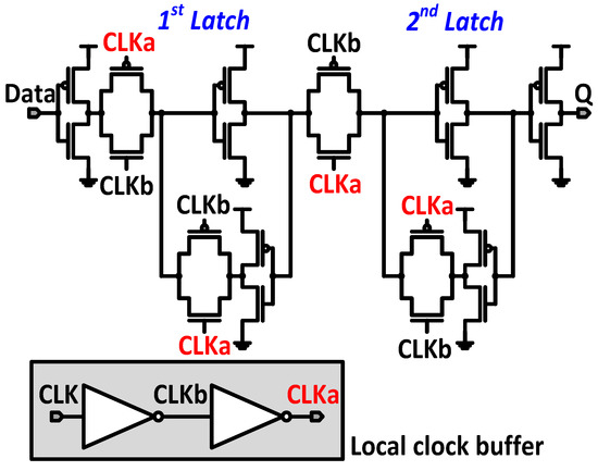
Figure 1.
Transmission Gate Flip-Flop (TGFF).
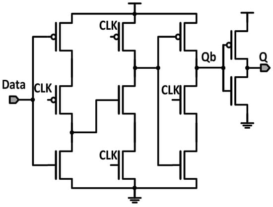
Figure 2.
True Single Phase Clock Flip-Flop (TSPCFF).
To improve the circuit performance at low power supply voltage, a 24T static single-phase contention-free flip-flop (S2CFF) shown in Figure 3 has been published [5]. The S2CFF can eliminate many glitches and maintain single-phase clock operation. Thus, the authors have described that the performance of S2CFF is much better than that of TSPCFF. However, it is still suffering from high power consumption because the continuous internal transitions of the node (the red line of net2 in Figure 3) are lastly undergoing. When the input data is low, the net2 is just following the clock. It means there is high power consumption. To minimize those internal transitions of S2CFF, a 24T change-sensing flip-flop (CSFF) shown in Figure 4 has been proposed [6]. Since the CSFF uses a change-sensing scheme, it can reduce the internal transitions. However, the power consumption might be significantly increased if the short circuit currents are generated at the node (the blue line of DNCS in Figure 4). The timing diagram of internal node (net2) transitions is shown in Figure 5. The timing diagram of CSFF is also shown in Figure 5. When the input data is high, the CS node (the red line in Figure 4) fluctuates. It means that huge power consumption can be generated at the high data activity ratio.
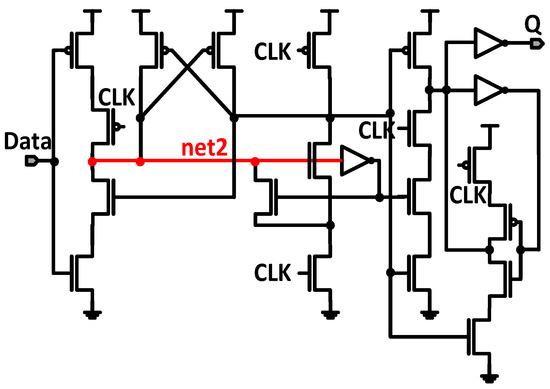
Figure 3.
Static Single-phase Contention-free Flip-Flop (S2CFF).
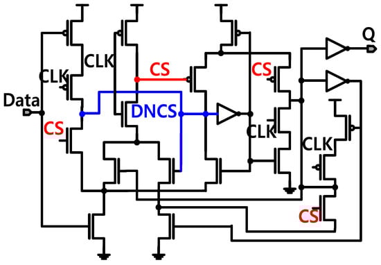
Figure 4.
Change-Sensing Flip-Flop (CSFF).
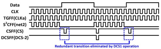
Figure 5.
Timing Diagram of Redundant Transitions between the Proposed One and Others.
In order to reduce power consumption with a wide dynamic voltage range, a flip-flop should satisfy the design requirements as follows. (1) Static operation: dynamic nodes are susceptible to process, voltage, and temperature variations at low power supply voltages. (2) contention-free transitions: ratioed logics may have serious unstable conditions with the wide range voltage swing. (3) Single-phase clocking: it avoids toggling the internal clock inverters and corresponding power penalty. (4) Small chip area: the chip size of the new FF should be smaller than that of conventional FFs. Even though various kinds of FFs to satisfy the requirements have been reported [8,9,10,11,12,13,14,15,16], a new scheme is proposed in this paper. The contents of this paper are as follows. In Section 2, a new FF is described and analyzed. The measured results are discussed in Section 3, and the conclusions are described in Section 4, respectively.
2. Proposed Dual Change-Sensing Flip-Flop (DCSFF)
Figure 6 shows the circuit diagram of the proposed dual change-sensing flip-flop (DCSFF). The aim of DCSFF is to minimize the power consumption by the reduction of internal transitions and the elimination of short-circuit currents that generate glitches in CSFF. Notably, since the continuous internal transitions are caused by CLK without the influence of output node, Q of FFs, those redundant transitions result in an increase of dynamic power consumption. The timing diagram which demonstrates the redundant transitions of conventional FFs is shown in Figure 5. The TGFF shows continuous redundant transitions due to the local clock buffer (CLKa and CLKb), whereas net2 of S2CFF involves continuous redundant transitions only when the data are “0”. The CS nodes of CSFF shown in Figure 4 reduce the redundant transitions compared to those of S2CFF because the redundant transitions only occur at the data transitions. To significantly minimize those redundant transitions, the proposed DCSFF divides CS nodes into two nodes (DCS-1 and DCS-2). DCS-1 and DCS-2 replace CS nodes when the data are rising and falling, respectively. The redundant transitions of CSFF and DCSFF generated by the data and CLK have four states shown in Figure 7. DCS-1 can eliminate the redundant transition when the input data are rising (Data = “0” to “1”). Compared to the conventional FFs, therefore, the proposed DCSFF has the least redundant transitions, which results in the minimum dynamic power consumption.
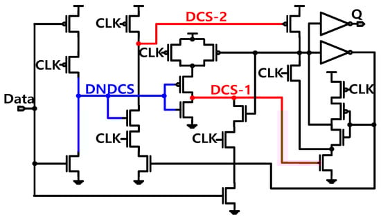
Figure 6.
Circuit Diagram of Proposed Dual Change-Sensing Flip-Flop (DCSFF).
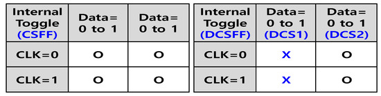
Figure 7.
Comparison of Internal Toggle Transitions between DCSFF and CSFF.
The left side of Figure 8a shows the process of glitch generation due to the short-circuit current in the CSFF. When the CLK maintains the “1” state, the CS node is discharged to detect the input data rising. As the input data changes “0” to “1”, the discharge path of DNCS is generated. Thus, a huge short-circuit current is generated with the glitch of DNCS, although the CS is discharged before the DNCS is discharged to maintain a value of “1”. Further, the DNCS should not retain the “1” state to eliminate the mechanism by which the short-circuit current in the CSFF is generated. On the contrary, the operation principle of the proposed DCSFF is shown in Figure 8b. The DNDCS of DCSFF is a similar node to the DNCS. In the same way, the DCSFF allows DCS-1 to hold “0”, even if the DNDCS is discharged without maintaining “1”. Therefore, no additional operation is required to maintain “1” in the DCSFF. As shown in Figure 8c, while DNCS has a serious short-circuit current, the DNDCS does not generate a short-circuit current, even if CLK remains in the “1” state when data are rising with DCS-1. Therefore, the proposed DCSFF reduces the dynamic power consumption by half compared to CSFF. Furthermore, the proposed DCSFF consumes less power than that of CSFF when the data activity ratio is high.
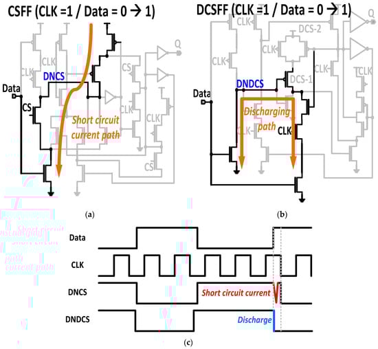
Figure 8.
Circuit Diagram of (a) CSFF and (b) DCSFF and (c) Comparison of Timing Diagram.
3. Measured Results
In order to implement an accurate comparison between conventional FFs and the proposed DCSFF, efficient on-chip testing circuits to measure many performance parameters should be considered. For example, the considered parameters are the power consumption, setup time, hold time, C-Q delay, data activity factor, etc. The measurement blocks are designed to realize the on-chip testing of each parameter. The setup and hold time measurement block is shown in Figure 9, which consists of a delay chain and an external monitoring block to encode the outputs and predict the internal skews [17]. Figure 10 shows the C-Q delay measurement block [18,19,20]. It has a ring oscillator structure, and the C-Q delay can be measured when we consider the difference in the frequency between the device under test (DUT) and reference rings. Figure 11 shows the power consumption measurement block. For the power consumption measurement block, the data activity factor is designed to be regulated. The initial external patterns are applied to the DUT periodically with a constant pulse signal. The data activity can be adjusted to range from 0% to 100% in 10% intervals.
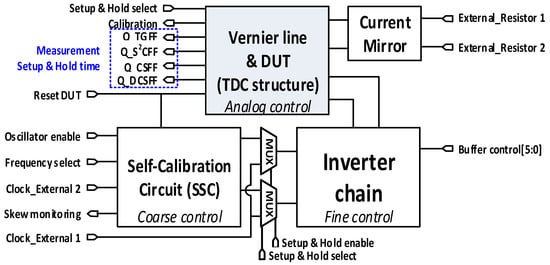
Figure 9.
Block Diagram for Setup and Hold Time Measurement.
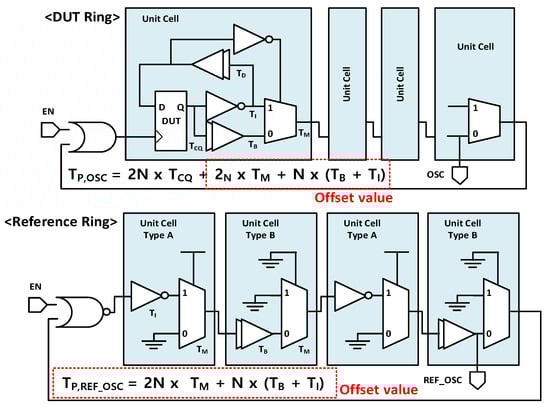
Figure 10.
Block Diagram of Power Measurement.
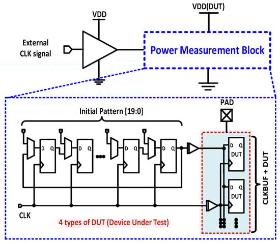
Figure 11.
Block Diagram of Power Measurement.
The layout drawing of the fabricated chip and testing PCB is shown in Figure 12. The proposed DCSFF has been fabricated with a Samsung 65-nm CMOS process with TGFF, S2CFF, and CSFF. All of them have been measured on the same chip. The setup and hold time measurement block shown in Figure 9 is placed at the right top side of Figure 12a. C-Q delay measurement block shown in Figure 10 is placed at the left top side of Figure 12a. Finally, the power measurement block shown in Figure 11 is placed at the left middle side of Figure 12a. Each block has the conventional FFs and the proposed DCSFF. The testing printed circuit board (PCB) with a fabricated chip is shown in Figure 12b.
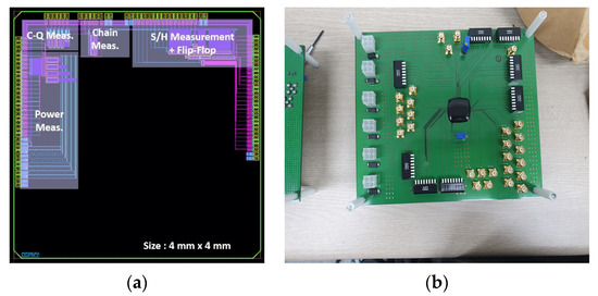
Figure 12.
(a) Chip Layout; (b) Testing PCB with a Fabricated Chip.
Figure 13 shows the measured power consumption, according to the increase of data activity ratio from 0% to 100%. The power consumptions of each FF have been measured under two conditions: (a) 1.2 V/100 MHz and (b) 0.5 V/10 MHz. In terms of data activity ratios, the CSFF and DCSFF almost do not consume power at 0% data activity ratio (=no leakage) because the drastic reduction of internal transition nodes is available. Thus, the CSFF and DCSFF have low absolute power consumption, even though the TGFF and S2CFF have a large power consumption when the data activity ratio is low. At the data activity ratio of 0%, for example, the power consumption of DCSFF is smaller by 94% than that of S2CFF from Figure 13a,b. Further, at the data activity ratio of 20%, for example, the power consumption of DCSFF is smaller by 78% than that of S2CFF from Figure 13a,b. By the way, since the CSFF is more sensitive to the data activity ratio than that of DCSFF, the slope of power consumption of CSFF is steeper by about 26% than that of DCSFF. When the data activity is 20%, the DCSFF has a 22.1% and 22% lower power consumption at 1.2 V/100 MHz and 0.5 V/10 MHz, respectively, compared to the CSFF. When the data activity is 100%, the power consumption of DCSFF is smaller by 26% than that of the CSFF.
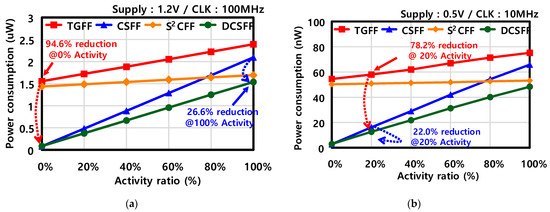
Figure 13.
Measured Power Consumption. (a) 1.2 V Supply and 100 MHz Clock (b) 0.5 V Supply and 10 MHz Clock.
However, the slope of power consumption of CSFF and DCSFF is two or three times steeper than that of TGFF and S2CFF, according to the increase of data activity ratios. At the data activity ratio of 100%, the power consumption of CSFF is bigger by 20% than that of S2CFF, and smaller by 15% than that of TGFF. However, the power consumption of the proposed DCSFF is always smaller than that of TGFF, S2CFF, and CSFF. Figure 14 shows the comparison data of the active energy consumption at the data activity ratio of 100%. The active energy of DCSFF is reduced by 35.7% and 26.6% compared to that of the TGFF and CSFF, respectively. Further, the active energy consumption of DCSFF is smaller by 11% than that of S2CFF. Therefore, the proposed DCSFF has the lowest power consumption among other conventional ones.
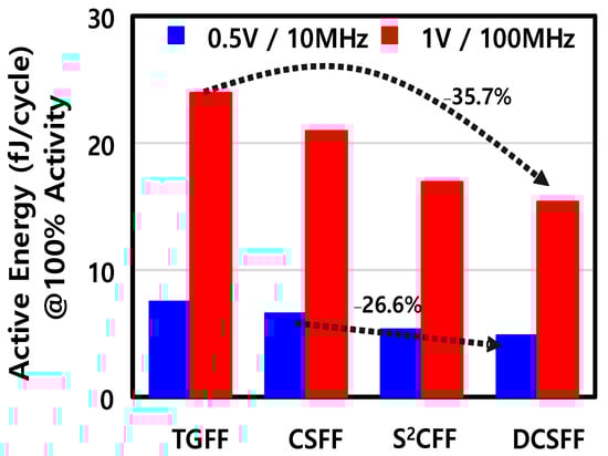
Figure 14.
Comparisons for Measured Active Energy.
Table 1 shows the measurement comparison table between the proposed DCSFF and other FFs. Since the proposed DCSFF is contention-free and composed of 24 transistors with a single phase clock, it is easy to design a circuit diagram and a layout drawing. When the layout size of the TGFF is normalized to 1, the area is increased by 5% for S2CFF, by 13% for CSFF, and by only 4% for DCSFF. It means the layout size of DCSFF is smaller by 8% than that of CSFF. The measured C-Q delay of DCSFF is 112.7 pico-seconds, which is the shortest among other FFs. However, the measured setup time and hold time is 216 pico-seconds and 49 pico-seconds, respectively. It means the proposed DCSFF has a disadvantage from the viewpoint of operating speed. At 100 MHz clock with 1.2 V power supply, the measured power consumption is 0.37 μW and 1.54 μW at the activity ratio of 20% and 100%, respectively. At 10 MHz clock with a 0.5 V power supply, the measured power consumption is 0.013 μW and 0.048 μW at the activity ratio of 20% and 100%, respectively. Further, the measured leakage power consumption is only 0.084 μW at a 1.2 V power supply. It means, in terms of power consumption, the proposed DCSFF has an excellent advantage compared to that of other ones. Therefore, the proposed DCSFF is suitable for ultra-low power system chips.

Table 1.
Performance Comparison Table between DCSFF and Other Ones.
4. Conclusions
In this paper, the design of a dual change-sensing flip-flop (DCSFF) to reduce dynamic power consumption and short circuit currents was described. Since the DCSFF has minimized the internal transition nodes shown in TGFF and SSCFF, there was no dynamic power consumption when the data activity was 0%. In addition, we proposed a new technique where a node to detect data changes in the CSFF has been separated into DCS-1 node and DCS-2 node, respectively. It reduced the internal transitions to detect the low to high of the data signal. At the same time, the glitch generated from the CSFF has been removed to reduce short circuit currents. Therefore, the dynamic power consumption and short-circuit currents of DCSFF have been drastically reduced. Finally, DCSFF had the lowest power consumption compared to other FFs in all sections of data activity. We expect that the proposed DCSFF could play a significant role in developing future ultra-low-power systems.
Author Contributions
Conceptualization, formal analysis, J.-Y.P. and M.J.; writing—original draft preparation, S.-Y.K.; supervision, M.S. All authors have read and agreed to the published version of the manuscript.
Funding
This work was supported in part by the Dongguk University Research Fund of 2020 and in part by National R&D Program through the National Research Foundation of Korea (NRF) funded by Ministry of Science and ICT (2022M3F3A2A01037928), and in part by the Technology development Program (S3196805) funded by the Minitry of SMEs and Startups(MSS, Korea).
Institutional Review Board Statement
Not applicable.
Informed Consent Statement
Not applicable.
Data Availability Statement
Not applicable.
Acknowledgments
The chip fabrication and EDA Tool were supported by the IC Design Education Center (IDEC).
Conflicts of Interest
The authors declare no conflict of interest.
References
- Yuan, J.; Hwang, B. High-Speed CMOS Circuit Technique. IEEE J. Solid-State Circuits 1989, 24, 62–70. [Google Scholar] [CrossRef] [Green Version]
- Shin, J.L.; Golla, R.; Li, H.; Dash, S.; Choi, Y.; Smith, A.; Sathianathan, H.; Joshi, M.; Park, H.; Elgebaly, M.; et al. The Next Generation 64b SPARC Core in a T4 SoC Processor. IEEE J. Solid-State Circuits 2013, 48, 82–90. [Google Scholar] [CrossRef]
- Markovic, D.; Tschanz, J.W.; De, V.K. Transmission-Gate Based Flip-Flop. U.S. Patent 6,642,765, 4 November 2003. [Google Scholar]
- Teh, C.K.; Fujita, T.; Hara, H.; Hamada, M. A 77% Energy-Saving 22-Transistor Single-Phase Clocking D-Flip-Flop with Adaptive-Coupling Configuration in 40nm CMOS. In Proceedings of the 2011 IEEE International Solid-State Circuits Conference, San Francisco, CA, USA, 20–24 February 2011; pp. 338–339. [Google Scholar]
- Kim, Y.; Shin, B. A static contention-free single-phase-clocked 24T flip-flop in 45nm for low-power applications. In Proceedings of the 2014 IEEE International Solid-State Circuits Conference Digest of Technical Papers (ISSCC), San Francisco, CA, USA, 9–13 February 2014; pp. 466–467. [Google Scholar]
- Le, V.L.; Li, J.; Chang, A.; Kim, T.H. A 0.4-V, 0.138-fJ/cycle single-phase-clocking redundant-transition-free 24T flip-flop with change-sensing scheme in 40-nm CMOS. IEEE J. Solid-State Circuits 2018, 53, 2806–2817. [Google Scholar] [CrossRef]
- Stojanovic, V.; Oklobdzija, V.G. Comparative analysis of masters-lave latches and flip-flops for high-performance and low-power systems. IEEE J. Solid-State Circuits 1999, 34, 536–548. [Google Scholar] [CrossRef]
- Alioto, M.; Consoli, E.; Palumbo, G. Variations in nanometer CMOS flip-flops: Part I—Impact of process variations on timing. IEEE Trans. Circuits Syst. I Regul. Pap. 2015, 62, 2035–2043. [Google Scholar] [CrossRef]
- Cai, Y.; Savanth, A.; Prabhat, P.; Myers, J.; Weddell, A.S.; Kazmierski, T.J. Ultra-low power 18-transistor fully static contention-free single-phase clocked flip-flop in 65-nm CMOS. IEEE J. Solid-State Circuits 2019, 54, 550–559. [Google Scholar] [CrossRef]
- Kawai, N.; Ishinura, M. A fully static topologically-compressed 21-transistor flip-flop with 75% power saving. IEEE J. Solid-State Circuits 2014, 49, 2526–2533. [Google Scholar] [CrossRef]
- Le, V.L.; Li, J.; Chang, A.; Kim, T.H. An 82% energy-saving change-sensing flip-flop in 40 nm CMOS for ultra-low power applications. In Proceedings of the 2017 IEEE Asian Solid-State Circuits Conference (A-SSCC), Seoul, Korea, 6–8 November 2017; pp. 197–200. [Google Scholar]
- Shin, G.; Lee, E.; Lee, J.; Lee, Y.; Lee, Y. A redundancy eliminated flip-flop in 28 nm for low-voltage low-power applications. IEEE Solid-State Circuits Lett. 2020, 3, 446–449. [Google Scholar] [CrossRef]
- Kuamar, H.; Nagarajan, R. Low Power High Speed 15-Transistor Static True Single Phase Flip Flop. In Proceedings of the 2nd International Conference on Intelligent Computing, Instrumentation and Control Technologies (ICICICT), Kannur, India, 5–6 July 2019; pp. 440–444. [Google Scholar]
- Lee, Y.; Shin, G.; Lee, Y. A Fully Static True-Single-Phase-Clocked Dual-Edge-Triggered Flip-Flop for Near-Threshold Voltage Operation in IoT Applications. IEEE Access 2020, 8, 40232–40245. [Google Scholar] [CrossRef]
- Huang, Y.; Jiao, H. An Ultra-Low-Voltage Single-Phase Adaptive Pulse Latch with Redundant Toggling Elimination. In Proceedings of the IEEE 15th International Conference on Solid-State & Integrated Circuit Technology (ICSICT), Kunming, China, 3–6 November 2020; pp. 1–3. [Google Scholar]
- Shin, G.; Lee, E.; Lee, J.; Lee, Y.; Lee, Y. An Ultra-Low-Power Fully-Static Contention-Free Flip-Flop With Complete Redundant Clock Transition and Transistor Elimination. IEEE J. Solid-State Circuits 2021, 56, 3039–3048. [Google Scholar] [CrossRef]
- Zhihong, L.; Yihao, Z.; Law, H. Self-calibrate two-step digital setup/hold time measurement. In Proceedings of the 2010 International Symposium on VLSI Design, Automation and Test, Hsin Chu, Taiwan, 26–29 April 2010; pp. 232–235. [Google Scholar]
- Giridhar, B.; Peterson, W. Pulse Amplification Based Dynamic Synchronizers with Meta-stability Measurement using Capacitance De-rating. In Proceedings of the IEEE 2013 Custom Integrated Circuits Conference, San Jose, CA, USA, 22–25 September 2013; pp. 110–113. [Google Scholar]
- Zhai, B.; Dreslinski, R.G.; Blaauw, D.; Mudge, T.; Sylvester, D. Energy efficient near-threshold chip multi-processing. In Proceedings of the 2007 International Symposium on Low Power Electronics and Design (ISLPED ’07), Portland, OR, USA, 27–29 August 2007; pp. 32–37. [Google Scholar]
- Wang, A.; Calhoun, B.; Chandrakasan, A. Sub-Threshold Design for Ultra Low-Power Systems; Springer: New York, NY, USA, 2006. [Google Scholar]
Publisher’s Note: MDPI stays neutral with regard to jurisdictional claims in published maps and institutional affiliations. |
© 2022 by the authors. Licensee MDPI, Basel, Switzerland. This article is an open access article distributed under the terms and conditions of the Creative Commons Attribution (CC BY) license (https://creativecommons.org/licenses/by/4.0/).