
Control of a Modified Switched-Capacitor Boost Converter


Abstract
:1. Introduction
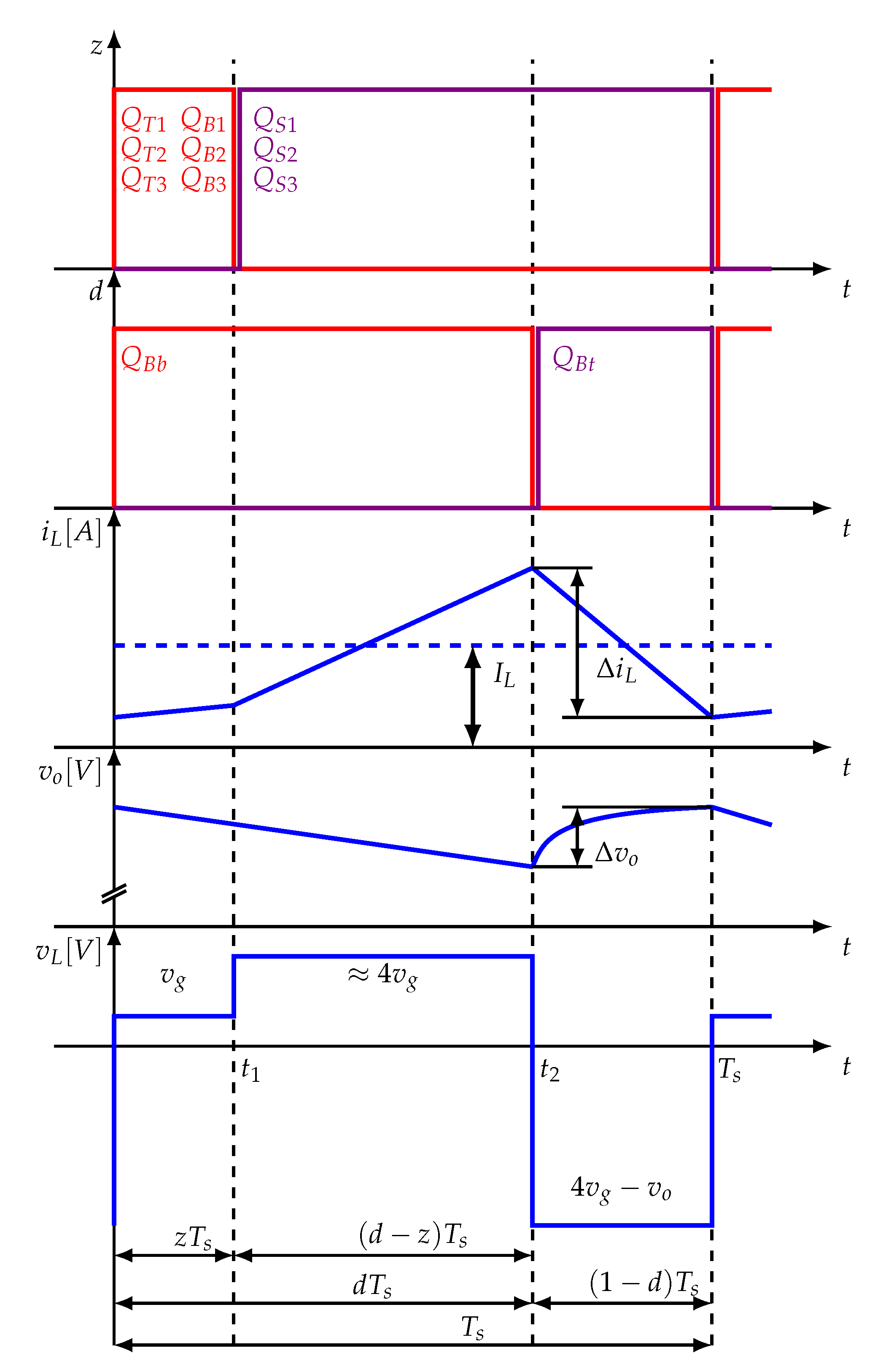
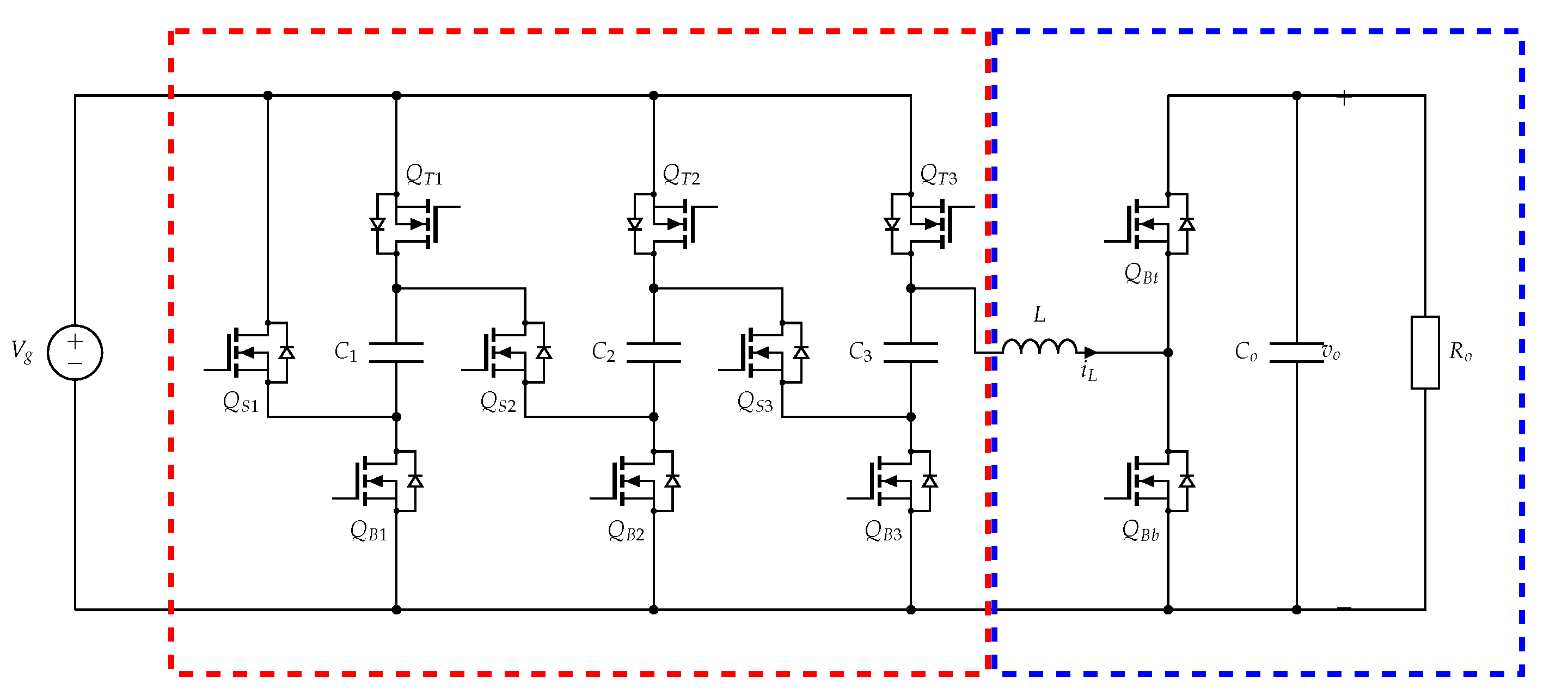
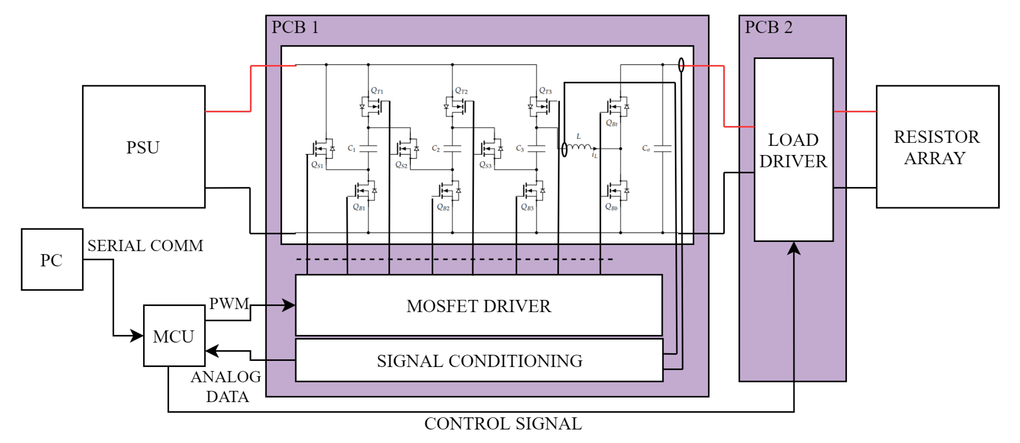
2. Operating Principles of the Converter
3. Converter Modelling
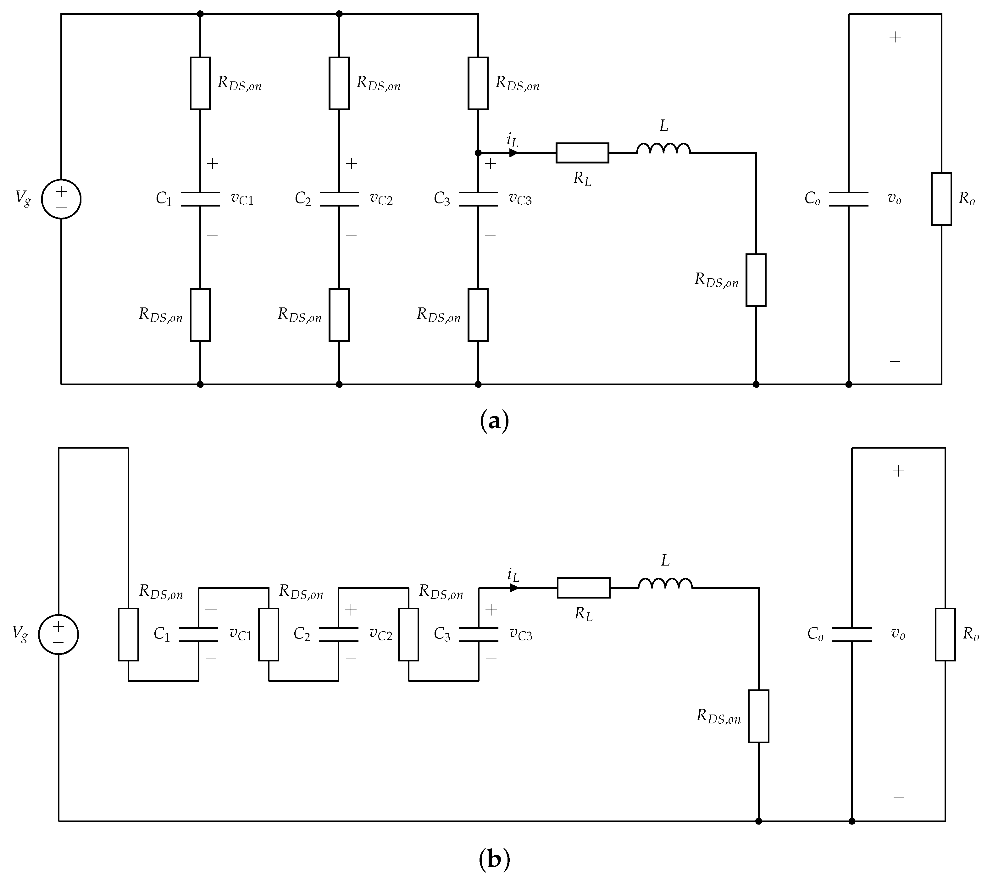
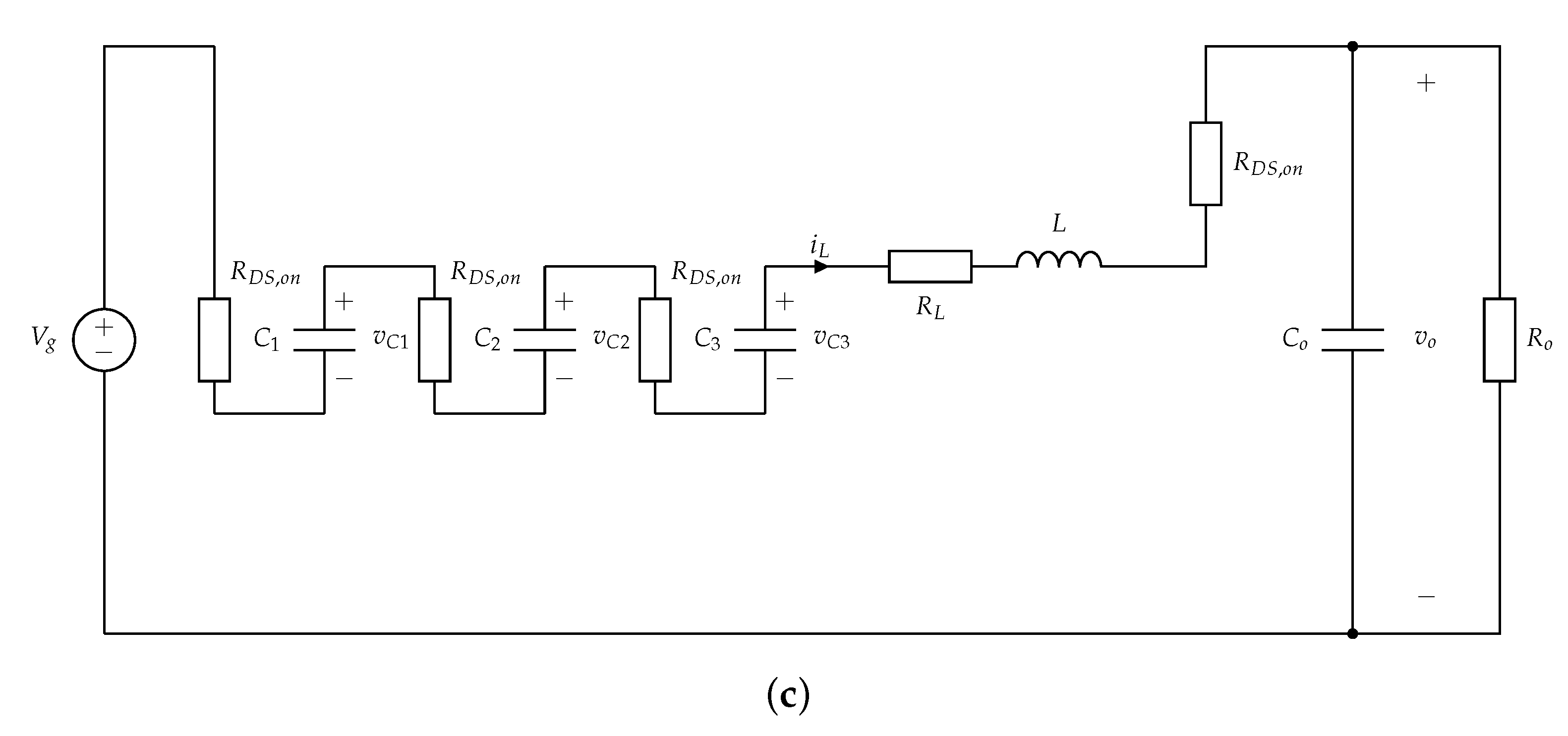
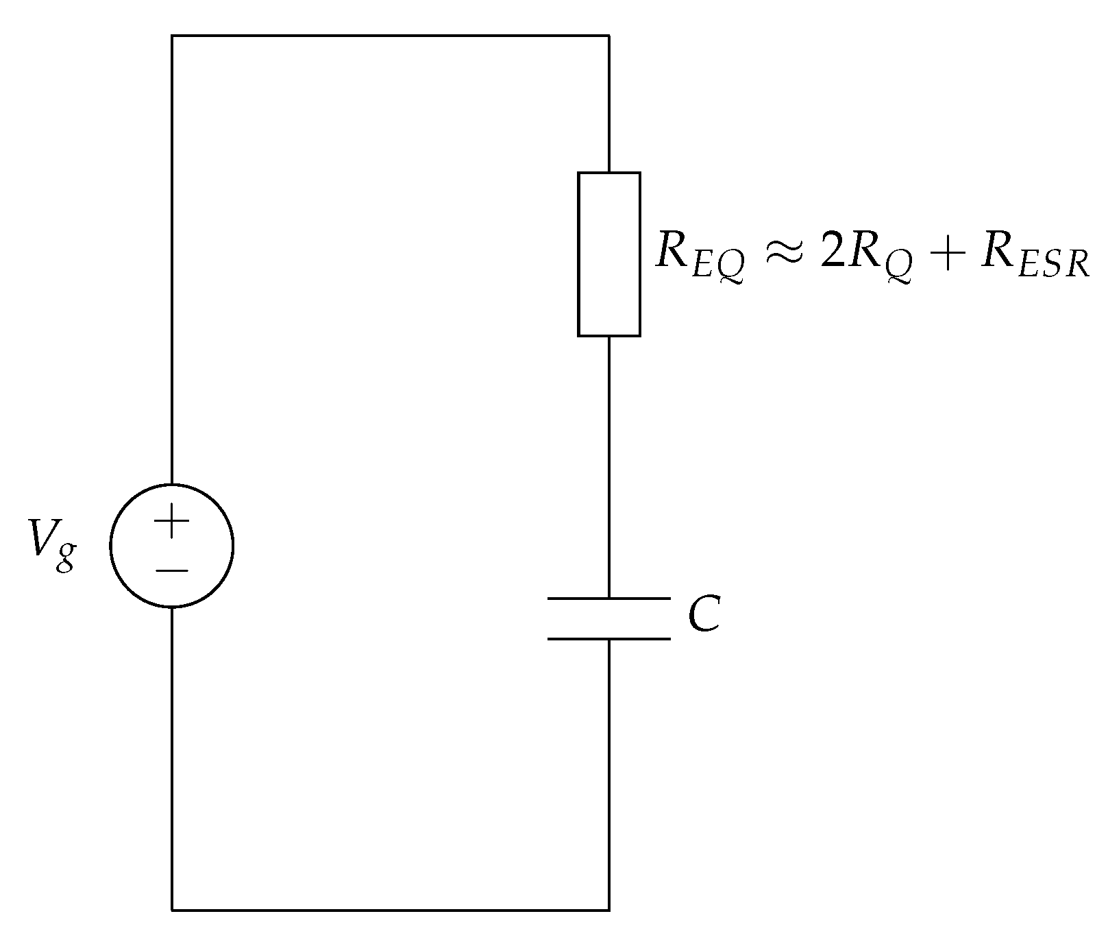
3.1. Mathematical Analysis
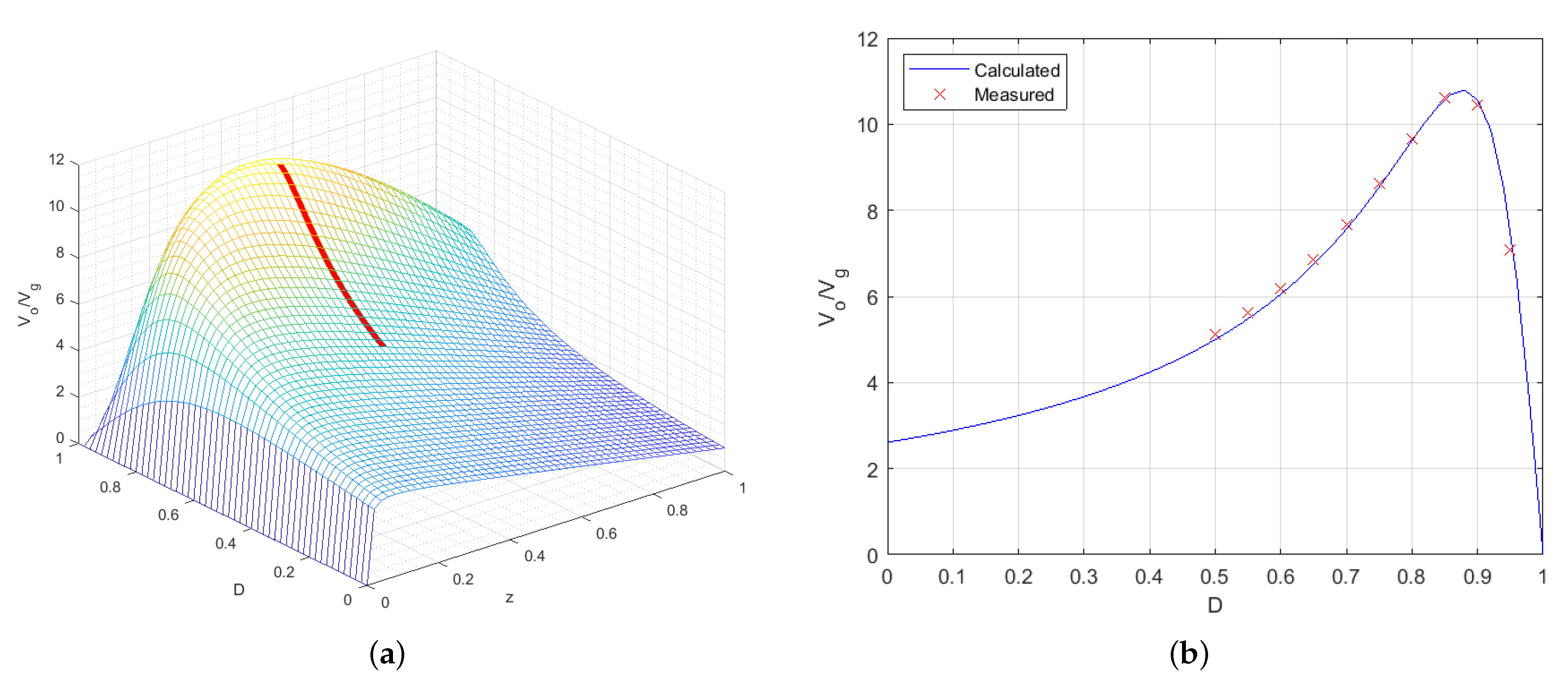
3.2. Design of Parameter Z
3.3. Comparison to Other Boost Structures
4. Control Algorithm
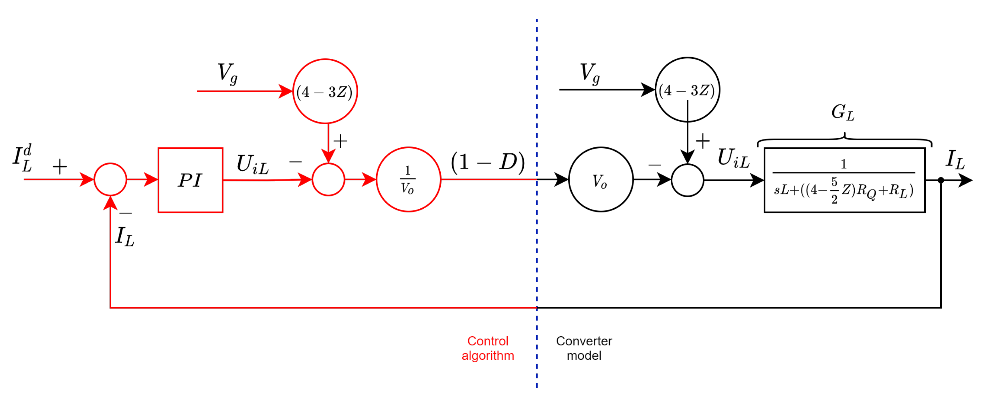
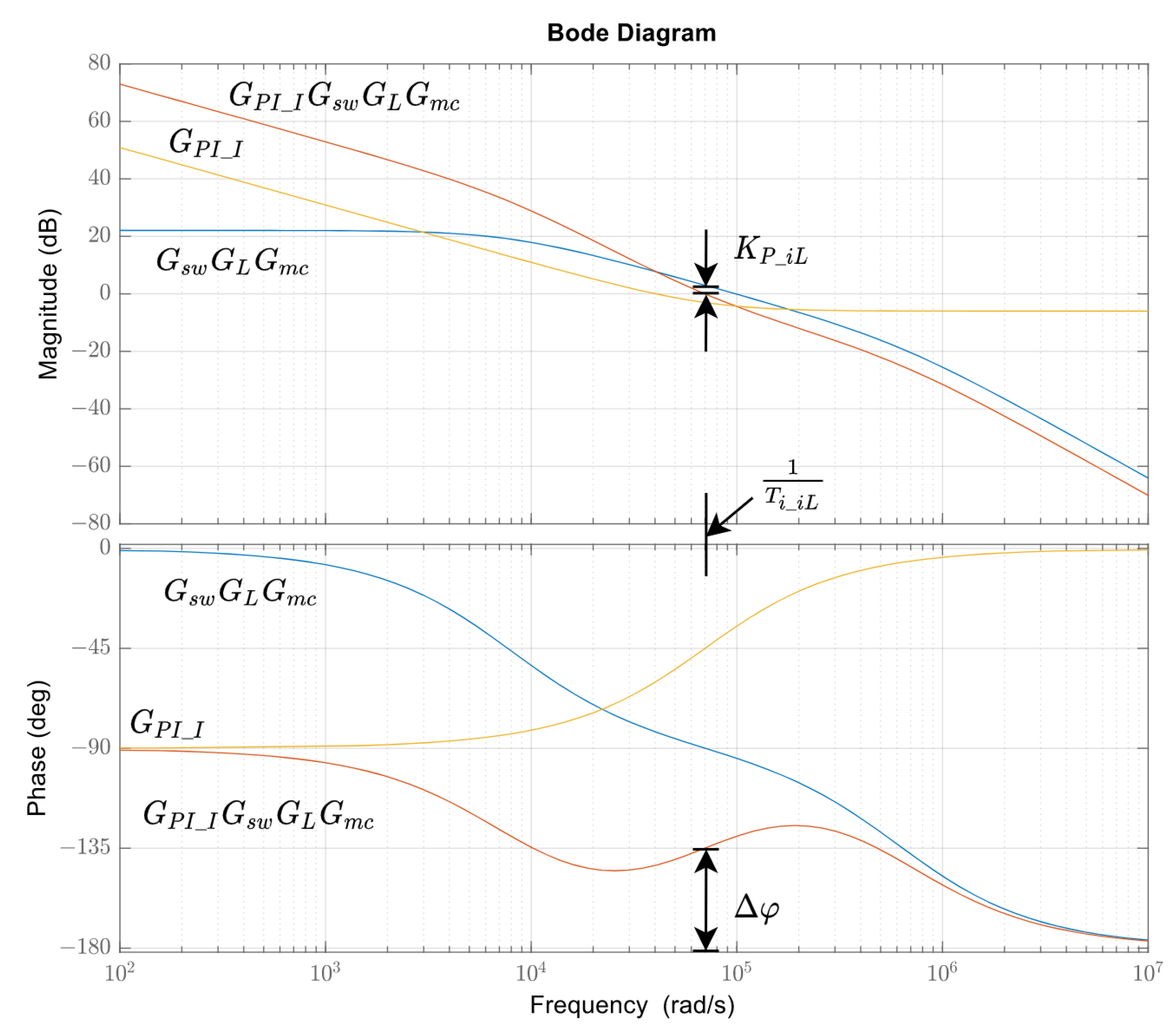
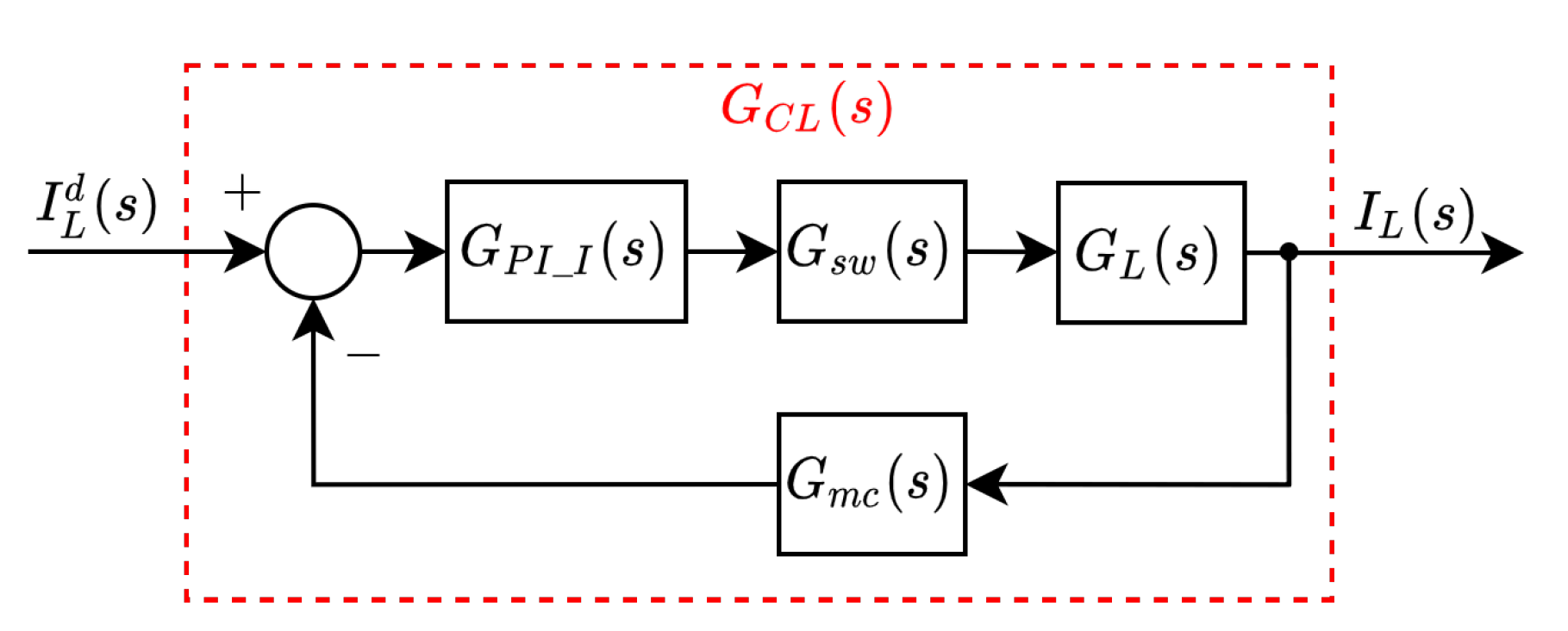
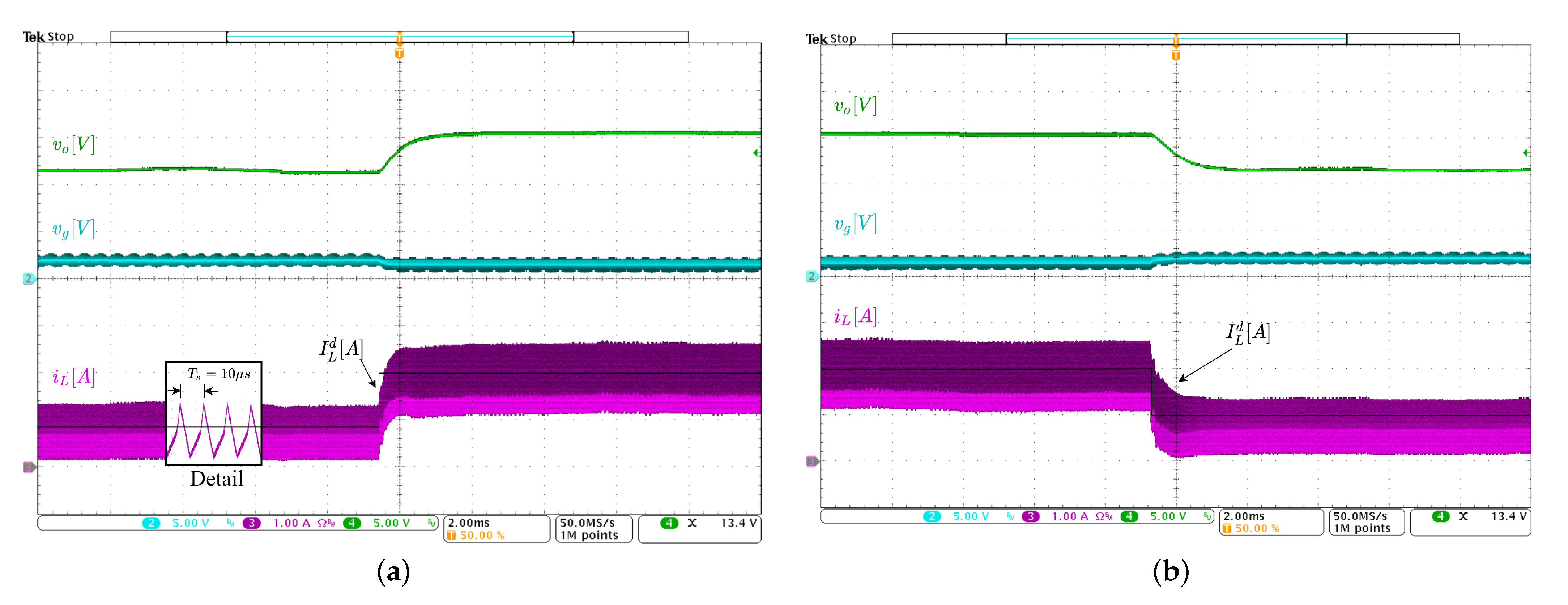
4.1. Inductor Current () Control
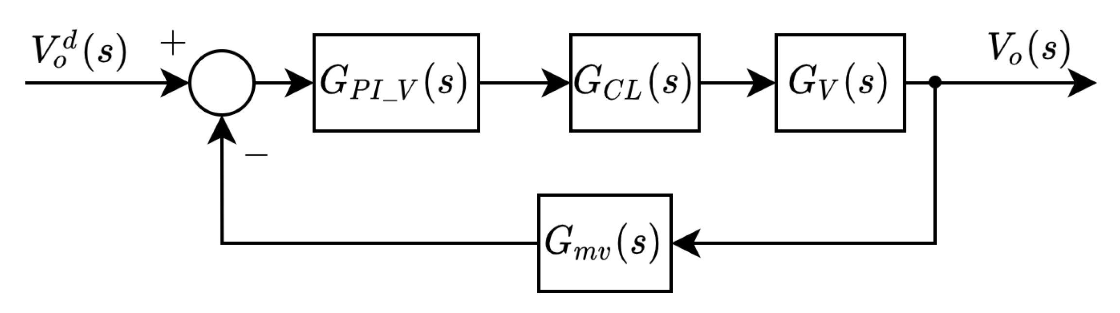
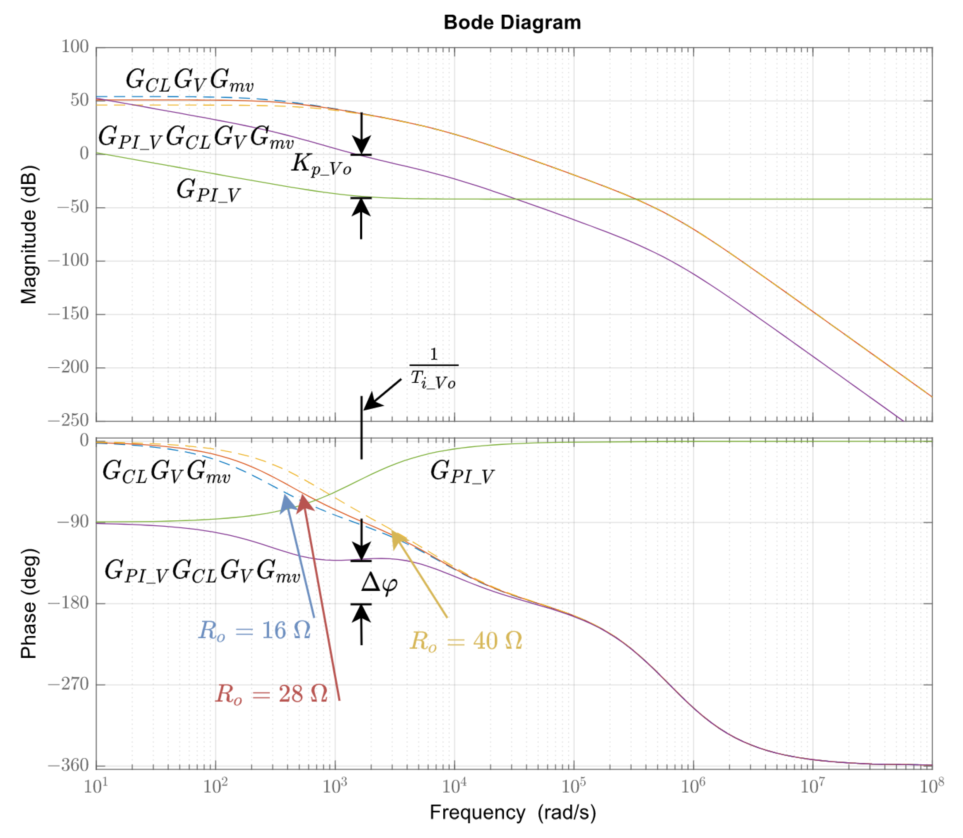
4.2. Output Voltage () Control
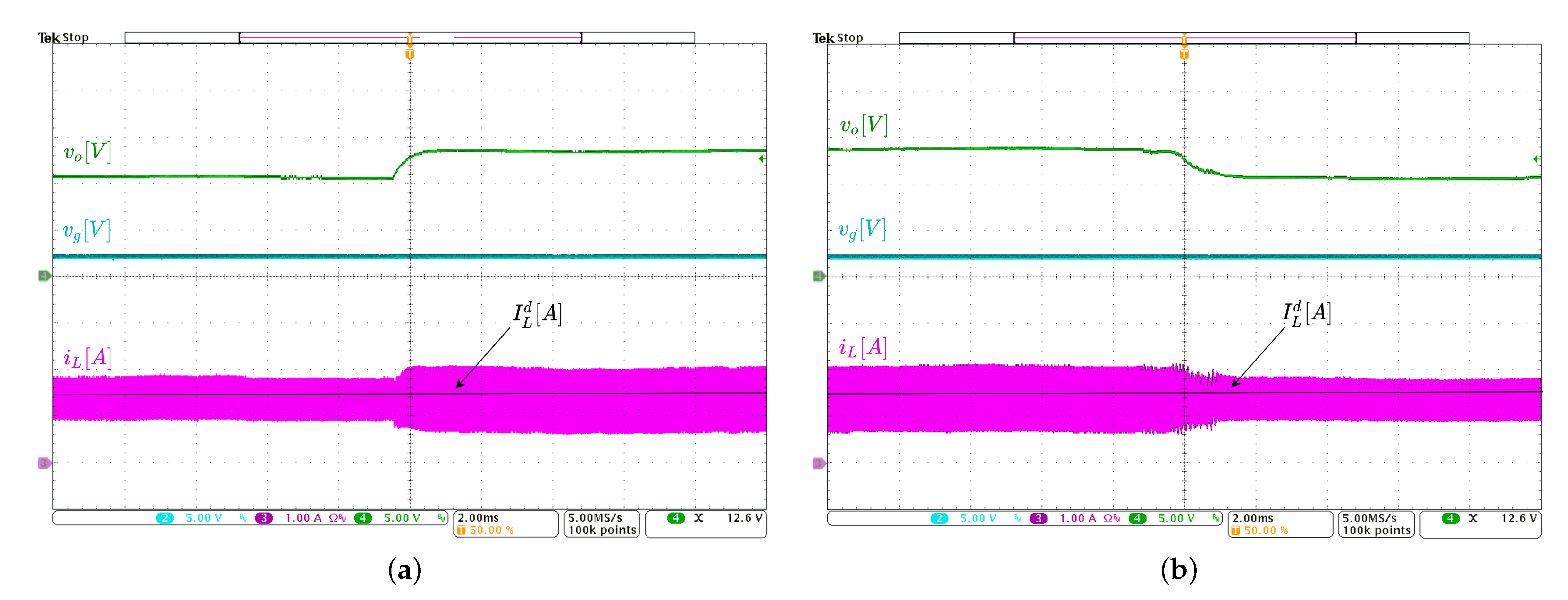
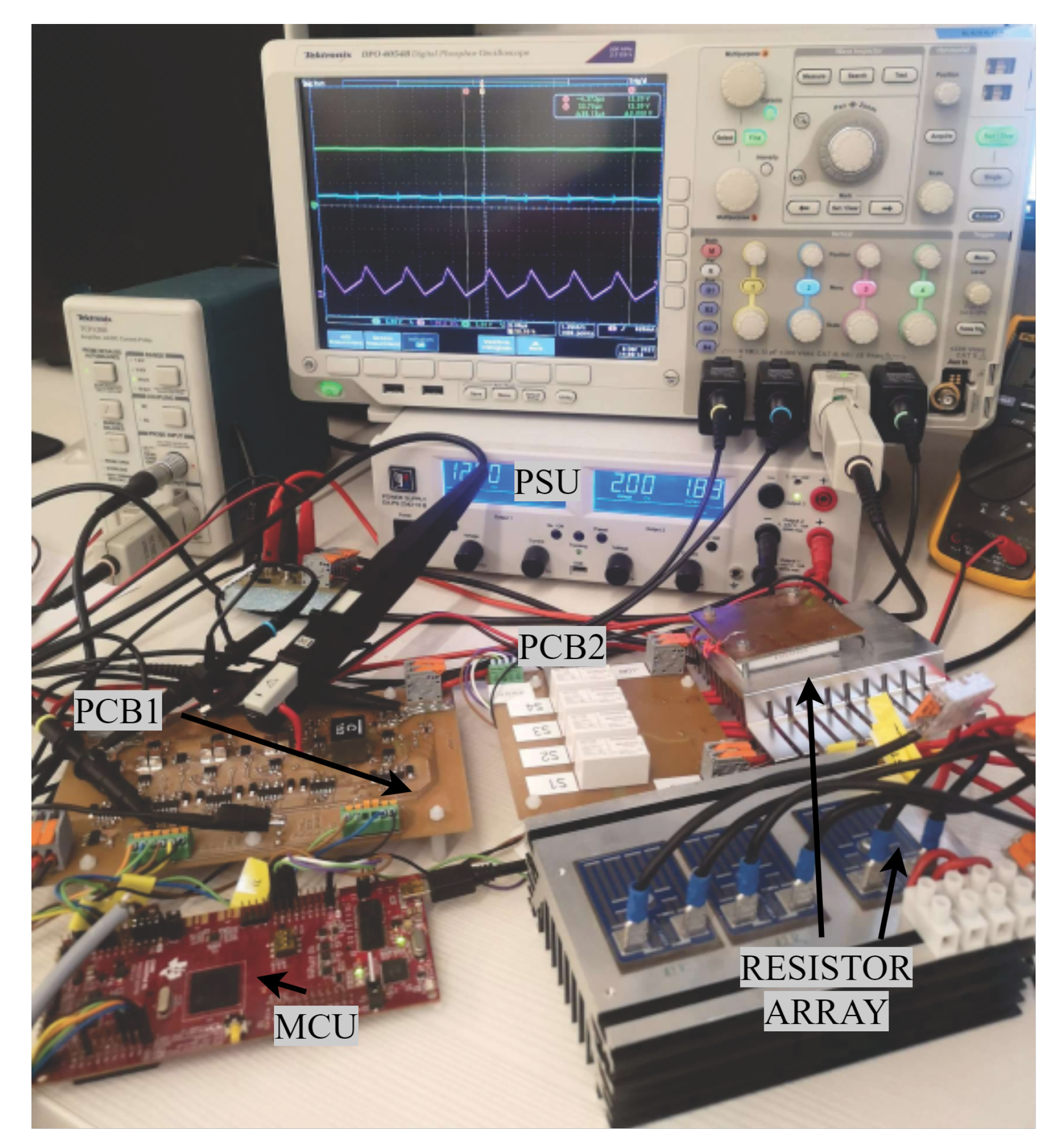
5. Results
5.1. Static Gain Verification
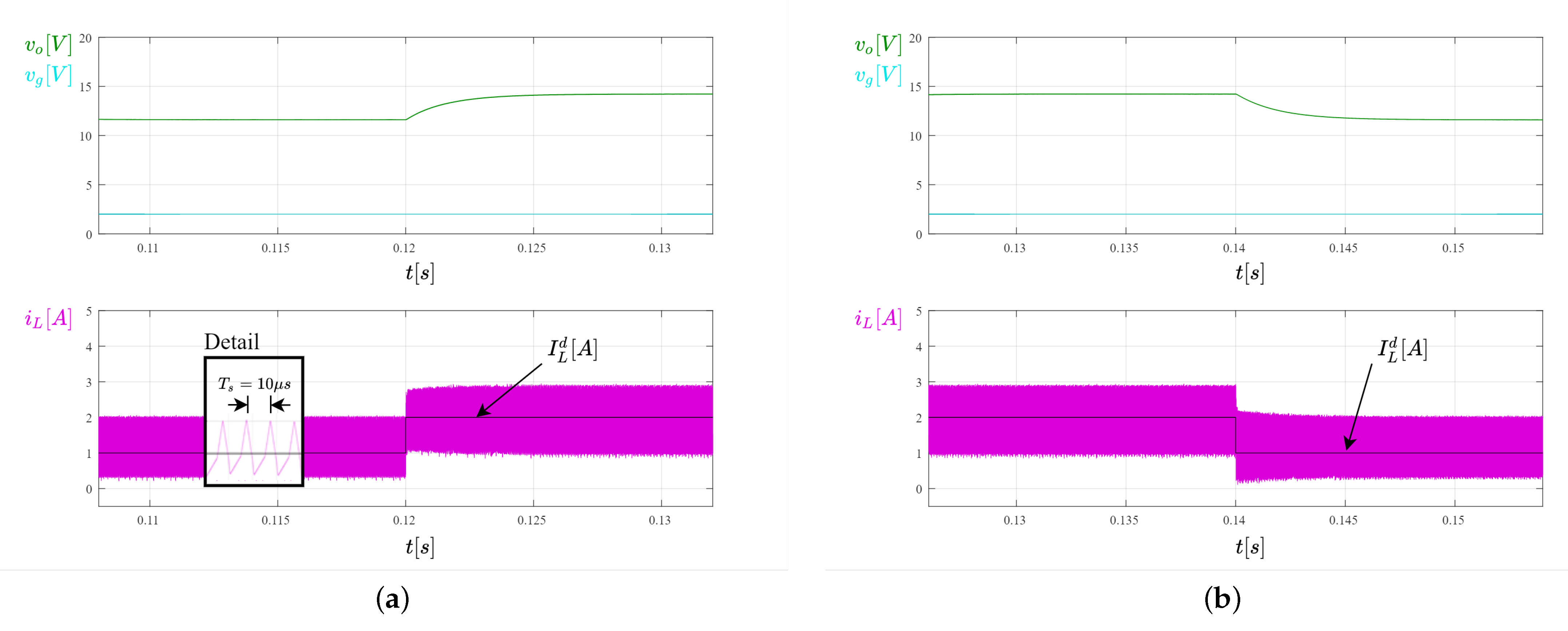
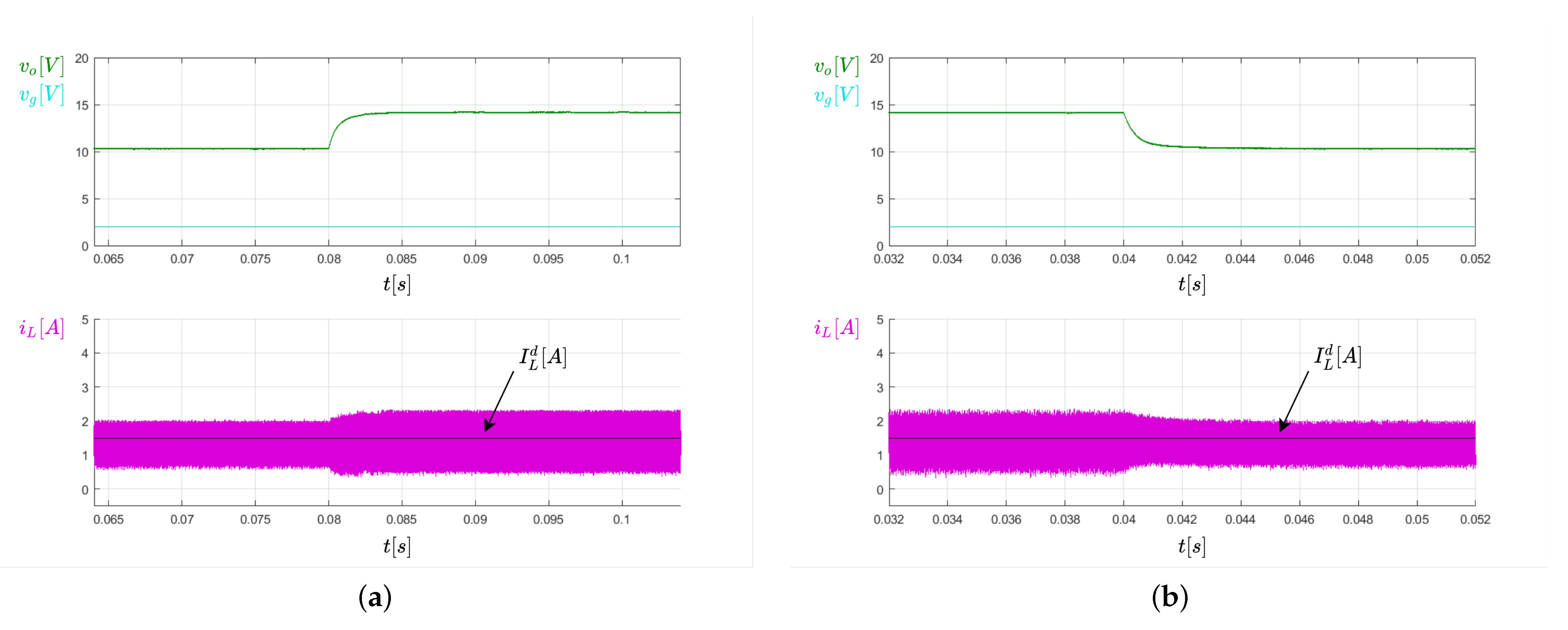
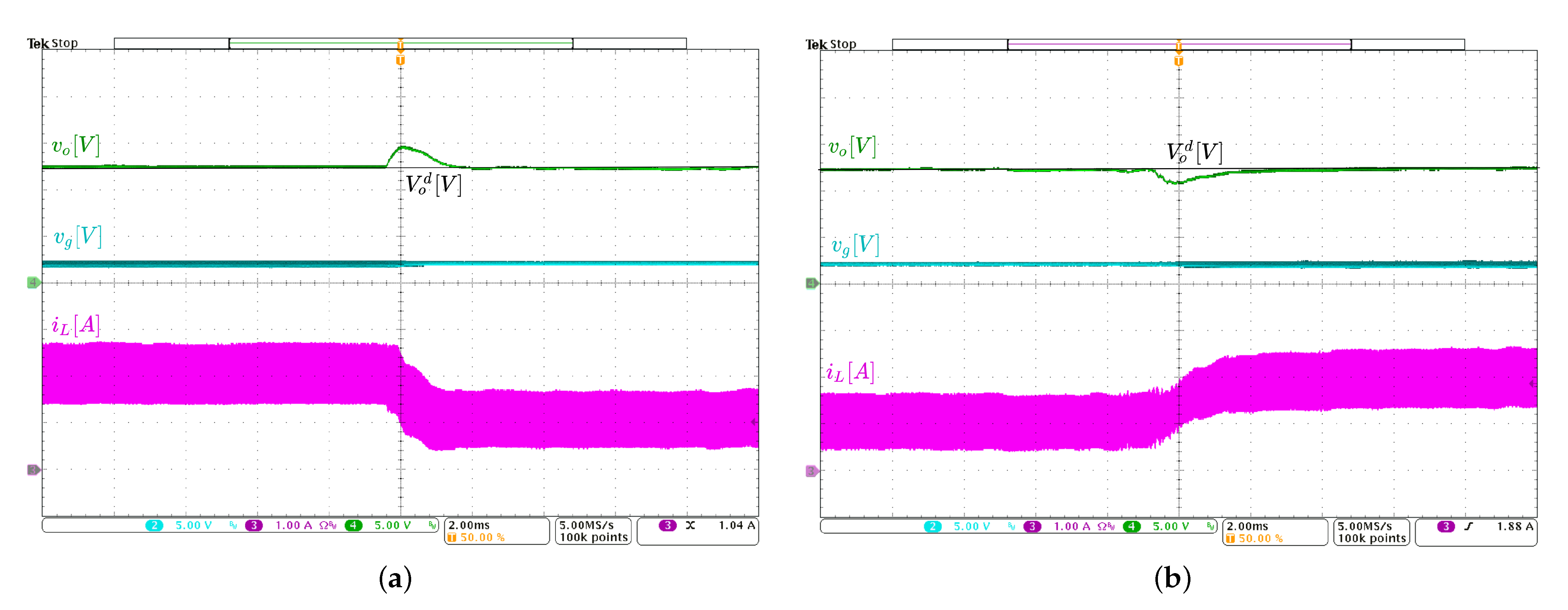
5.2. Inductor Current Control
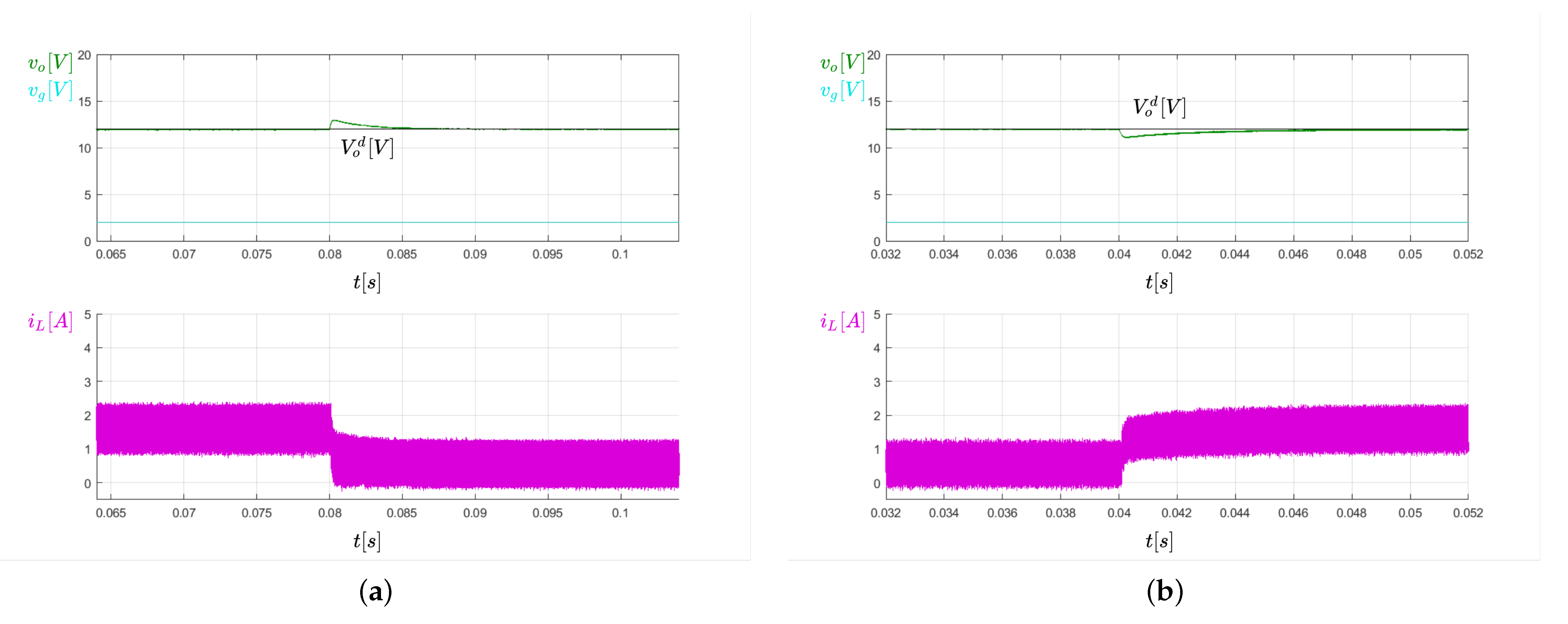
5.3. Output Voltage Control
5.4. Comparison of Control with Similar Converters
6. Discussion
Author Contributions
Funding
Conflicts of Interest
References
- Ioinovici, A. Switched-capacitor power electronics circuits. IEEE Circuits Syst. Mag. 2001, 1, 37–42. [Google Scholar] [CrossRef]
- Cao, D.; Qian, W.; Peng, F.Z. A high voltage gain multilevel modular switched-capacitor DC-DC converter. In Proceedings of the 2014 IEEE Energy Conversion Congress and Exposition (ECCE), Pittsburgh, PA, USA, 14–18 September 2014; pp. 5749–5756. [Google Scholar] [CrossRef]
- Lei, Y.; Liu, W.C.; Pilawa-Podgurski, R.C.N. An Analytical Method to Evaluate and Design Hybrid Switched-Capacitor and Multilevel Converters. IEEE Trans. Power Electron. 2018, 33, 2227–2240. [Google Scholar] [CrossRef]
- Jiang, S.; Nan, C.; Li, X.; Chung, C.; Yazdani, M. Switched tank converters. In Proceedings of the 2018 IEEE Applied Power Electronics Conference and Exposition (APEC), San Antonio, TX, USA, 4–8 March 2018; pp. 81–90. [Google Scholar] [CrossRef]
- Seeman, M.D.; Sanders, S.R. Optimization of Switched-Capacitor DC-DC Converters. IEEE Trans. Power Electron. I Regul. Pap. 2008, 23, 841–851. [Google Scholar] [CrossRef]
- Makowski, M.; Maksimovic, D. Performance limits of switched-capacitor DC-DC converters. In Proceedings of the PESC ’95—Power Electronics Specialist Conference, Atlanta, GA, USA, 18–22 June 1995; Volume 2, pp. 1215–1221. [Google Scholar] [CrossRef]
- Chang, Y.H. Variable-Conversion-Ratio Switched-Capacitor-Voltage-Multiplier/Divider DC-DC Converter. IEEE Trans. Circuits Syst. I Regul. Pap. 2011, 58, 1944–1957. [Google Scholar] [CrossRef]
- Abutbul, O.; Gherlitz, A.; Berkovich, Y.; Ioinovici, A. Step-up switching-mode converter with high voltage gain using a switched-capacitor circuit. IEEE Trans. Circuits Syst. I Fundam. Theory Appl. 2003, 50, 1098–1102. [Google Scholar] [CrossRef]
- Rodič, M.; Milanovič, M.; Truntič, M.; Ošlaj, B. Switched-Capacitor Boost Converter for Low Power Energy Harvesting Applications. Energies 2018, 11, 3156. [Google Scholar] [CrossRef] [Green Version]
- Middlebrook, R.D.; Ćuk, S. A general unified approach to modelling switching-converter power stages. Int. J. Electron. 1977, 42, 521–550. [Google Scholar] [CrossRef]
- Schaef, C.; Stauth, J.T. A 12-volt-input hybrid switched capacitor voltage regulator based on a modified series-parallel topology. In Proceedings of the 2017 IEEE Applied Power Electronics Conference and Exposition (APEC), Tampa, FL, USA, 26–30 March 2017; pp. 2453–2458. [Google Scholar] [CrossRef]
- Hamo, E.; Cervera, A.; Peretz, M.M. Multiple conversion ratio resonant switched-capacitor converter with active zero current detection. In Proceedings of the 2013 IEEE Energy Conversion Congress and Exposition, Denver, CO, USA, 5–19 September 2013; pp. 805–812. [Google Scholar] [CrossRef]
- Huber, L.; Jovanovic, M. A design approach for server power supplies for networking applications. In Proceedings of the APEC 2000. Fifteenth Annual IEEE Applied Power Electronics Conference and Exposition (Cat. No.00CH37058), New Orleans, LA, USA, 6–10 February 2000; Volume 2, pp. 1163–1169. [Google Scholar] [CrossRef] [Green Version]
- Rosas-Caro, J.C.; Ramirez, J.M.; Peng, F.Z.; Valderrabano, A. A DC–DC multilevel boost converter. IET Power Electron. 2010, 3, 129–137. [Google Scholar] [CrossRef]
- Mohan, N.; Undeland, T.M.; Robbins, W.P. Power Electronics: Converter, Application and Design; John Wiley & Sons: New York, NY, USA, 2002. [Google Scholar]
- Dodds, S.J. Feedback Control: Linear, Nonlinear and Robust Techniques and Design with Industrial Applications; Springer: London, UK, 2015. [Google Scholar]
- Truntič, M.; Konjedic, T.; Milanovič, M.; Šlibar, P.; Rodič, M. Control of integrated single-phase PFC charger for EVs. IET Power Electron. 2018, 11, 1804–1812. [Google Scholar] [CrossRef]
- Maruša, L.; Milanović, M.; Valderrama-Blavi, H. Evaluating a Switched Capacitor-Boost Converter (SC-BC) for energy harvesting in a Peltier-cells thermoelectric system. In Proceedings of the 2015 International Conference on Electrical Drives and Power Electronics (EDPE), High Tatras, Slovakia, 21–23 September 2015; pp. 227–234. [Google Scholar] [CrossRef]


| Characteristic | Topologies of Modular Boost Structures | |||
|---|---|---|---|---|
| Cascaded boost [13] | Multilevel boost [14] | High gain boost [8] | SC-BC | |
| Voltage stress across switches | ||||
| Static gain | ||||
| Number of switches | N, N > 1 | 1 | n + 2 | 3n + 2 |
| Duty cycle range | 0 < D < 1 | 0 < D < 1 | 0 < D < 1 | Z < D < 1 |
| Number of diodes | N | 2n + 1 | 2n + 1 | - |
| Number of capacitors | N | n + 1 | n + 1 | n + 1 |
| Operating frequency of magnetics | ||||
| Number of inductors | N | N | 1 | 1 |
| Boost modularity | yes | yes | yes | yes |
| D | ||
|---|---|---|
| 0.50 | 10.37 | 5.13 |
| 0.55 | 11.35 | 5.67 |
| 0.60 | 12.45 | 6.23 |
| 0.65 | 13.73 | 6.87 |
| 0.70 | 15.41 | 7.71 |
| 0.75 | 17.32 | 8.66 |
| 0.80 | 19.36 | 9.68 |
| 0.85 | 21.24 | 10.62 |
| 0.90 | 20.90 | 10.45 |
| 0.95 | 14.15 | 7.07 |
Publisher’s Note: MDPI stays neutral with regard to jurisdictional claims in published maps and institutional affiliations. |
© 2022 by the authors. Licensee MDPI, Basel, Switzerland. This article is an open access article distributed under the terms and conditions of the Creative Commons Attribution (CC BY) license (https://creativecommons.org/licenses/by/4.0/).
Share and Cite
Ošlaj, B.; Truntič, M. Control of a Modified Switched-Capacitor Boost Converter. Electronics 2022, 11, 654. https://doi.org/10.3390/electronics11040654
Ošlaj B, Truntič M. Control of a Modified Switched-Capacitor Boost Converter. Electronics. 2022; 11(4):654. https://doi.org/10.3390/electronics11040654
Chicago/Turabian StyleOšlaj, Benjamin, and Mitja Truntič. 2022. "Control of a Modified Switched-Capacitor Boost Converter" Electronics 11, no. 4: 654. https://doi.org/10.3390/electronics11040654
APA StyleOšlaj, B., & Truntič, M. (2022). Control of a Modified Switched-Capacitor Boost Converter. Electronics, 11(4), 654. https://doi.org/10.3390/electronics11040654