1. Introduction
The dual active bridge converter (DAB) has garnered great interest over the last 15 years [
1,
2,
3,
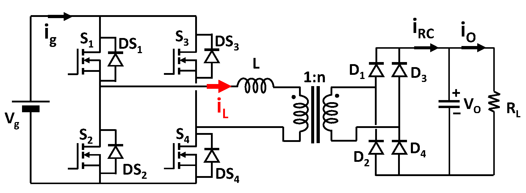
4]. Its input-output symmetry makes it especially interesting for applications where bidirectional power flow between the input and output ports is required. In applications where one of the ports will always act as the input and the other as the output, it is possible to replace the entire active output bridge with a diode bridge, lowering the cost of the converter. The converter thus obtained has been called the single active bridge (SAB). The general scheme of the SAB converter is shown in
Figure 1. Few studies have examined the basics of this converter [
5,
6,
7]; thus, a full study is warranted.
In recent years, different circuit topologies have been proposed for unidirectional isolated DC/DC converters, such as battery chargers. Multiple SAB converters are connected in the input-parallel and output-parallel (IPOP) configuration to achieve higher power in [
8]. In addition, an isolated three-port DC/DC converter based on SAB converters is proposed in [
9] to offer an efficient solution for meeting the increasing demand of integrating energy delivery elements, such as renewable energy sources, energy storage devices, and mains.
A different unidirectional topology, also based on the DAB converter in which two switches in the secondary H-bridge converter are replaced with diodes, is proposed in [
10] for fuel cell electric vehicles. Other topologies based on the SAB are analyzed in [
11], where the SAB with a voltage doubler and with a full-bridge rectifier are compared, and [
12] in which suitable modulation and controller schemes are proposed for improving the converter dynamics.
To improve the efficiency and power density of the SAB converter, soft-switching capabilities of this converter in its different conduction modes are analyzed in [
6,
13], and techniques to reduce switching and conduction losses are proposed in [
14,
15,
16].
This article describes an extensive study of the static characteristics of this converter, including its conduction modes and the boundary between them, the value of its voltage conversion ratio in each conduction mode, the determination of the electrical requirements of its semiconductors, a guide to its design, and a comparison with other similar topologies. This study was validated using simulation and experimental results.
2. Static Analysis of SAB Converter in Continuous Conduction Mode (CCM)
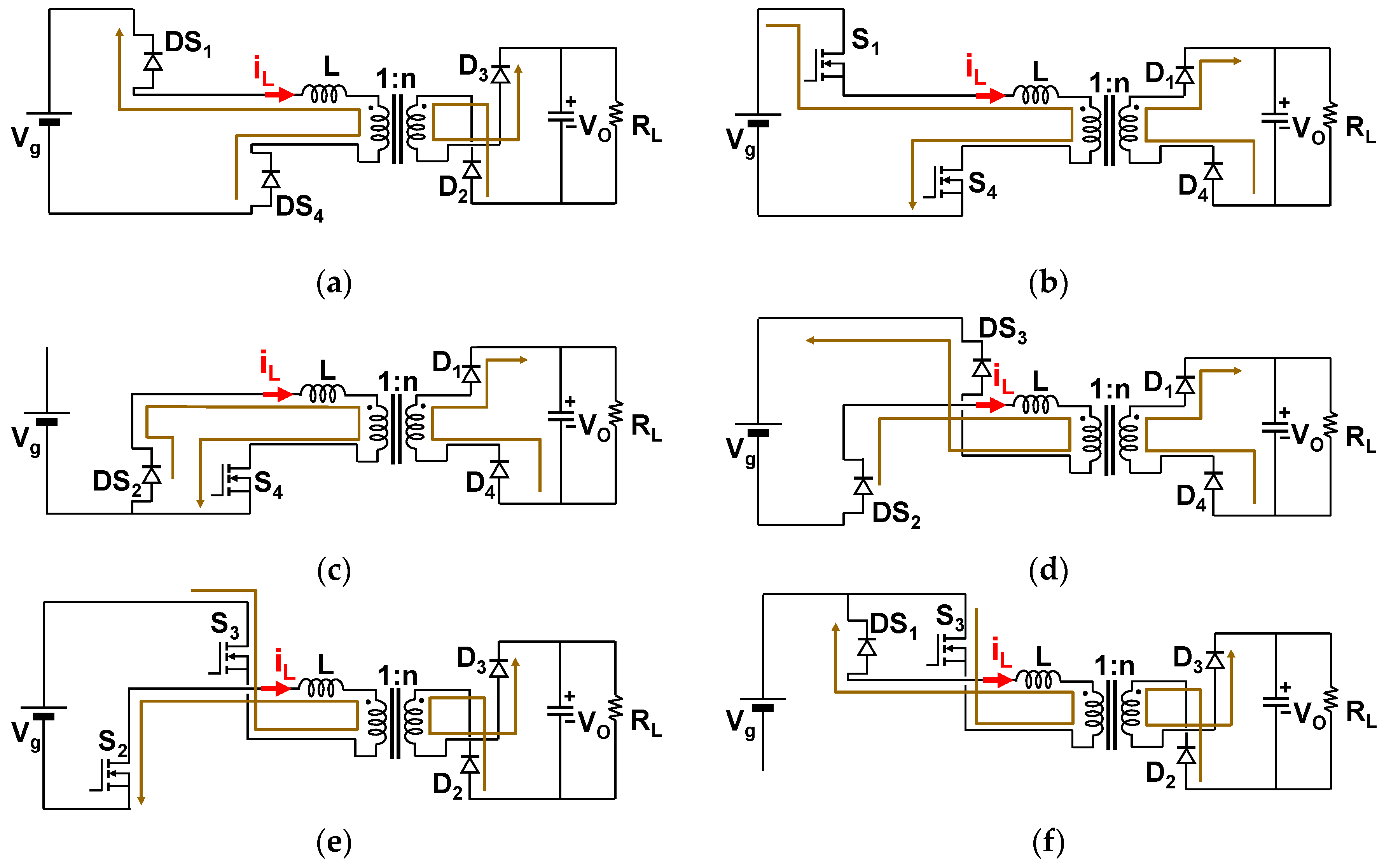
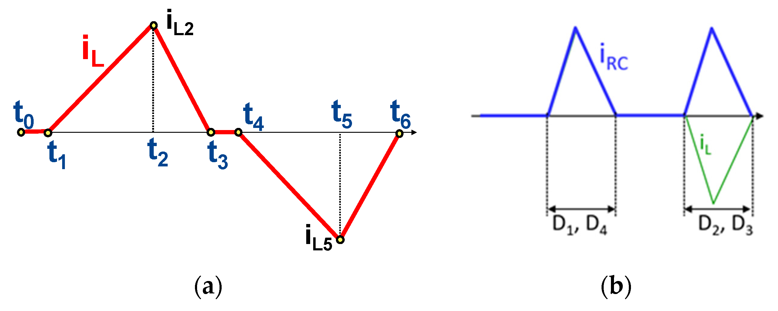
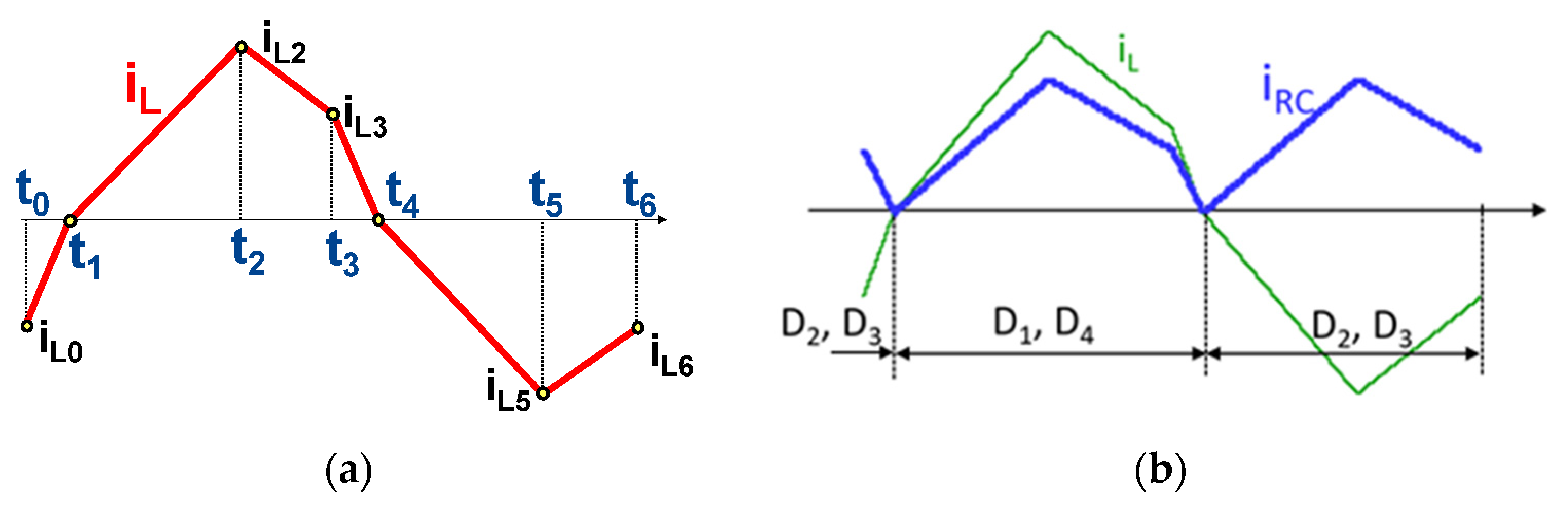
Figure 2 shows the six equivalent circuits that characterize the operation of the converter in the operation mode in which the current by the inductor does not remain at zero. This operation mode is called continuous conduction mode (CCM). The value of the current passing through the inductor (
iL), shown in
Figure 3a, can be calculated in all cases applying Faraday’s law. The results are as follows:
- Interval (
t0,
t1): Corresponds to
Figure 2a, where the semiconductors conducting the current are DS
1, DS
4, D
2, and D
3. The value of
iL is:
where
iL0 is the inductor current value at the beginning of this interval. This interval ends when
iL reaches zero at
t1, the value of which is:
- Interval (
t1,
t2): Corresponds to
Figure 2b, where the semiconductor conducting the current are S
1, S
4, D
1, and D
4. The value of
iL is:
At the end of this interval, the inductor current reaches the value
iL2 at instant
t2, the value of which is:
- Interval (
t2,
t3): Corresponds to
Figure 2c, where the semiconductors conducting the current are DS
2, S
4, D
1, and D
4. The value of
iL is:
At the end of this interval, the inductor current reaches the value
iL3 = −
iL0 at instant
t3, the value of which is:
- Interval (
t3,
t4): Corresponds to
Figure 2d, where the semiconductors conducting the current are DS
2, DS
3, D
1, and D
4. The value of
iL is:
This interval ends when
iL reaches zero at instant
t4, the value of which is:
- Interval (
t4,
t5): Corresponds to
Figure 2e, where the semiconductors conducting the current are S
2, S
3, D
2, and D
3. The value of
iL is:
At the end of this interval, the inductor current reaches the value,
iL5 = −
iL2, at instant
t5, the value of which is:
- Interval (
t5,
t6): Corresponds to
Figure 2f, where the semiconductors conducting the current are DS
1, S
3, D
2, and D
3. The value of
iL is:
At the end of this interval, the inductor current reaches the value,
iL6 = −
iL3, at instant
t6, the value of which is:
Finally, the switching period can be obtained as a result of the duration of these intervals using:
Given the operation symmetry of the converter in periods, (
t0,
t3) and (
t3,
t6), the following equation is satisfied:
One of the possible control techniques for this converter is to keep the frequency constant and to regulate the duration of the time corresponding to intervals, (
t0,
t1) and (
t1,
t2). For this reason, it is useful to define:
The voltage conversion ratio of this converter in this conduction mode can be calculated using the previous equations, determining the average current injected into the output RC network,
iRC_avg, during a switching half period, which for convenience can be measured between
t1 and
t4. Note that during this entire time interval, D
1 and D
4 diodes are conducting; thus, the
iL/n current is injected into the aforementioned RC network. Since the
iL waveform is composed of linear sections, this calculation is quite simple, but laborious. The result of the calculation is:
This current determines the output voltage value, given by the following equation:
Using Equations (16)–(18), the normalized voltage conversion ratio is easily obtained using:
where
N is the voltage conversion ratio normalized at the transformer ratio (
n) and parameter
k is defined as:
Equations (19) and (20) show that the SAB converter has high output impedance operating in CCM, as its voltage conversion ratio depends on the load resistance, RL, through the parameter k. This situation (a behavior similar to a current source) is the opposite of most DC/DC converters operating in CCM. This is because the inductor is placed on the AC side of the converter and not at the output of the rectifier, as in other bridge converters. The operation of the SAB converter in CCM only implies that the current does not remain at zero when it reaches this value.
3. Static Analysis of SAB Converter in Discontinuous Conduction Mode (DCM)
The operation mode in which the current passing through the inductor reaches zero in the intervals, (
t2,
t3) and (
t5,
t6), is called discontinuous continuous mode (DCM). If this occurs, the current remains zero until the end of these intervals. In this case, some of the equations for CCM must be modified. Thus, Equations (1) and (7) for CCM become, in both cases:
The value of
iL given by the previous equations in the other intervals remains valid. The duration of the different intervals, given by (2) and (8) are not valid, while Equations (4) and (10) remain unchanged, and Equations (6) and (12) must be modified by replacing the values of
iL3 and
iL6 with zero. The linear subcircuits of
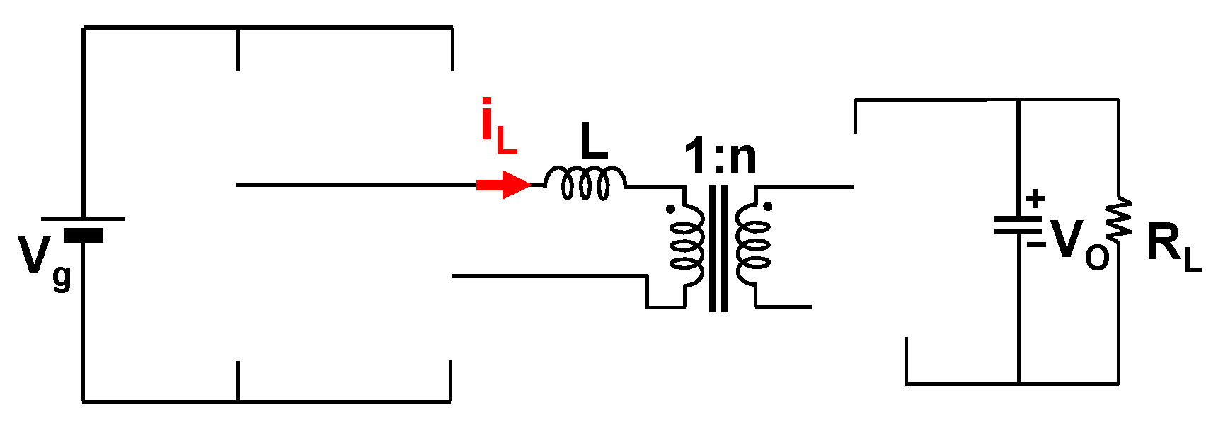
Figure 2a,d are no longer valid and must be replaced by the one depicted in
Figure 4. The
iL waveform in DCM is represented in
Figure 5a.
As in CCM, the voltage conversion ratio is calculated in DCM using the value of
iRC_avg. The calculation of
iRC_avg is again simple but laborious. The result is as follows:
Using (16), (18), and (22), the normalized voltage conversion ratio in DCM is easily obtained:
4. Boundary between the Two Conduction Modes and Voltage Conversion Ratio
In the operation of the SAB converter working at a constant frequency, the value of the parameter,
k, varies only with the load resistance (
RL). The
RL value corresponding to the converter operating on the boundary between the two conduction modes is called
RL_crit.
kcrit can be defined as follows:
As Equations (19) and (23) must be simultaneously verified on the boundary between the two conduction modes, and adding the suffix “
crit” to the corresponding
k and
d values to operate at this boundary, the following equation is obtained:
By substituting Equation (25) in (19) or (23), the following equation is obtained:
As in the case of other converters, CCM occurs when RL < RL_crit. Considering Equation (24), this is equivalent to verifying in CCM, while in DCM.
Once the boundary between the two conduction modes has been obtained, it is straightforward to determine when (19) (valid only in CCM) and when (23) (valid only in DCM) should be used to calculate the open loop voltage conversion ratio. Setting the value of duty cycle
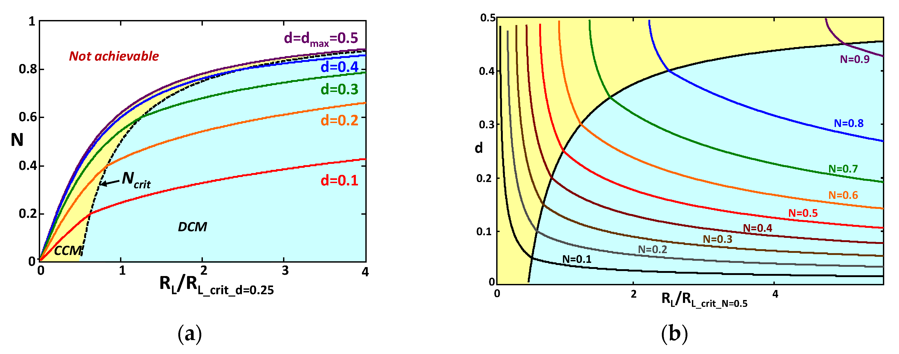
d and letting the output voltage change when changing
RL, the evolution of this normalized voltage conversion ratio is shown in
Figure 6a, which shows three different regions: operation in CCM, operation in DCM, and unachievable voltage conversion ratios.
Figure 6a shows that this converter has high output impedance, not only in DCM (as other converters) but also in CCM. This peculiar behavior can be interesting for certain applications. The maximum normalized voltage conversion ratio is obtained by unloading the converter to the limit, which corresponds to calculating the limit of
N (calculated in DCM, i.e., by (23)) as
k approaches zero:
The information provided by
Figure 6a is very important for understanding the operation of the SAB converter, but it is especially useful to have an idea of the closed-loop operation of the converter, that is, when a feedback loop ensures a given voltage conversion ratio at full load and the value of
RL is gradually increased. Under these conditions, the duty cycle of the converter will decrease, which can be seen in
Figure 6b. The normalized voltage conversion ratio,
N, has been used as a parameter. The duty cycle at the boundary of the two conduction modes,
dcrit, is the value shown in (26).
The curves shown in
Figure 6b are obtained using (19) and (23), clearing the value of
d. The value of
RL has been represented as normalized in
Figure 6b, using the critical value of
RL when
N is 0.5 as the base value for normalization. Remember that the maximum value of
N is 1, given by (27).
5. Voltage and Current Stresses of Semiconductors
One of the most interesting properties of this converter is that the maximum voltages in the transistors and diodes in the primary bridge, on the one hand, and in the diodes in the output rectifier bridge, on the other hand, are limited by the values of the input and output voltages, respectively.
In contrast, rms currents passing through the transistors and diodes of the primary bridge (in general, considering the possibility of using IGBTs) strongly depend on the point of operation of the converter and which of the branches is being considered. The latter is closely related to the sequence of control pulses in transistors.
As an example, an operation point has been chosen in CCM.
Figure 7a shows the voltages at the midpoints of the two branches of the bridge (v
S2 and v
S4). The phase-shift between them generates the v
B waveform, which is the voltage between those midpoints. Looking at the voltages, v
S2 and v
S4, it is clear that v
S2 is delayed from v
S4; thus, the branch where v
S2 is measured is called the “lagging branch”, and the other branch is called the “leading branch”.
From the sequence of intervals shown in
Figure 2, the waveforms in
Figure 7b are easily inferred. In the lagging branch there is a more equal distribution of the currents driven by the transistor and its diode in anti-parallel, compared to the leading branch. Therefore, conduction losses will be greater in transistors in the leading branch and in anti-parallel diodes of transistors in the lagging branch, than in transistors in the lagging branch and anti-parallel diodes of transistors in the leading branch.
Average and rms currents through the semiconductors of the primary bridge can be calculated using the following equations:
Average and rms currents through the diodes of the secondary bridge can be calculated using the following equations:
Average values of the input and output currents and the rms value of the inductor current can be calculated with the following equations:
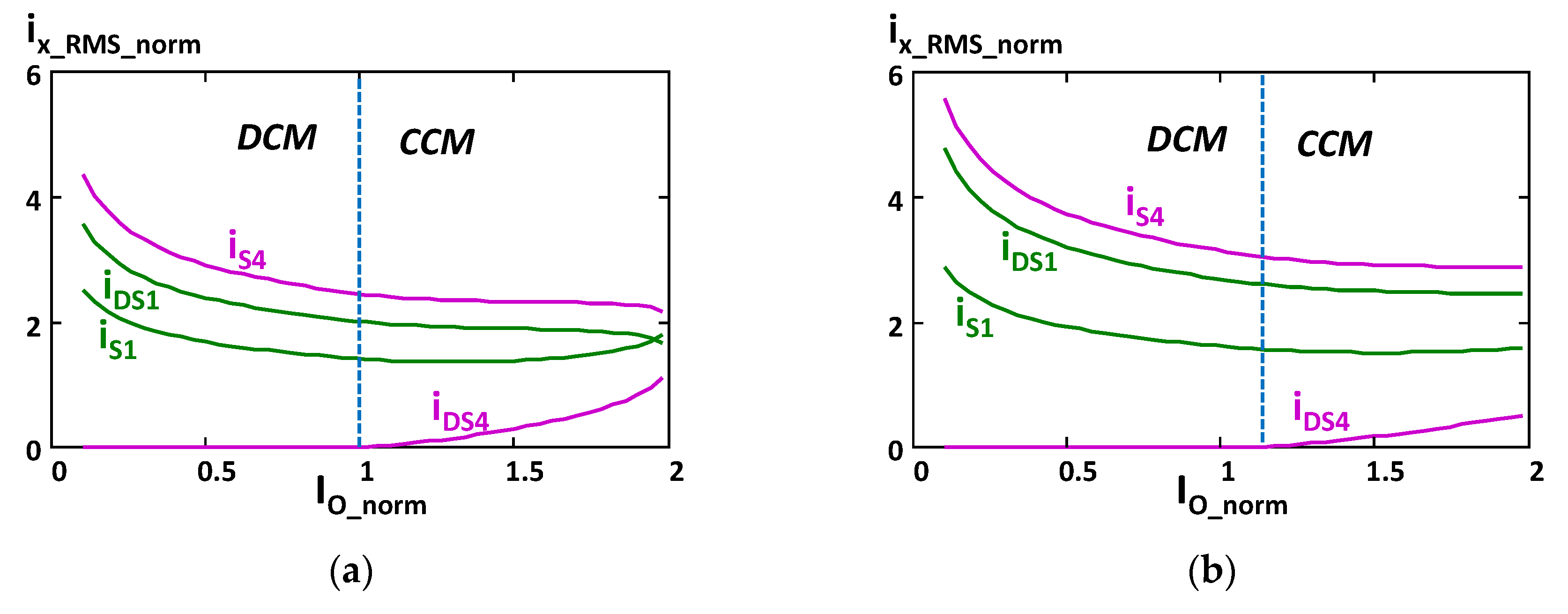
To graphically show the distribution of the currents through the transistor and its anti-parallel diode (
Figure 8), an SAB converter is designed, selecting the change between modes at half of the maximum output current for the lower input voltage and the higher output voltage (i.e., the maximum voltage conversion ratio). The semiconductor rms current values are normalized to the average input current, while the output current is normalized to its maximum value.
In
Figure 8a, normalized rms values of the current through the semiconductors are shown for the maximum voltage conversion ratio (
N =
Nmax), while in
Figure 8b, the voltages are changed to obtain a
N = 0.8·
Nmax.
Another important issue to consider is the possibility of operating with zero-voltage-switching (ZVS) on the transistors in the primary bridge. During the interval, (t0, t3), this is achieved if the iL current is positive in t2 and t3 since this current is responsible for redistributing the electrical charges associated with the parasitic capacitance of the midpoints of the branches. This current is always positive in t2 but is only positive in t3 if the converter operates in CCM. Of course, the same happens in the interval, (t3, t6), but in this case with iL being negative at t5 and t6. Therefore, transistors in the leading branch only operate with ZVS in CCM, while transistors in the lagging branch operate with ZVS in both conduction modes.
Consequently, the operation in CCM is desirable to minimize switching losses on the transistors. However, CCM implies that during intervals, (t0, t1) and (t3, t4), the iL current is not zero (unlike in DCM) and is circulating in such a way that electrical power is returned to the primary source (Vg). In other words, the converter works with electrical energy recirculated towards its input (reactive energy), which ends up decreasing its efficiency by increasing conduction losses. Therefore, the ideal situation is one in which the converter works in CCM but very close to the boundary between this mode and DCM.
Finally, rectifier diodes of the secondary bridge operate neglecting switching losses in both conduction modes. The current in the turn-off of the rectifier diodes is always zero, and consequently, there are no reverse recovery losses.
6. Comparison with Other Converters
As discussed above, the SAB converter operating in CCM differs markedly from similar DC/DC converters, as VO varies by changing the RL value when d and Vg are maintained constant. On the other hand, the operation in DCM is very similar to the other classic converters belonging to the buck family of converters, as will be explained in this section.
Regarding the SAB converter operating in the DCM, (23) can be rewritten as follows:
In the case of the buck converter operating in DCM, it is well known that the voltage conversion ratio in DCM is [
17]:
where the subscript “
Buck” has been added to the original expression given in [
17]. The value of the dimensionless conduction parameter
kBuck is defined in [
17] as follows:
Comparing (43) with (44) and (20) with (45), it can be concluded that N and NBuck coincide if:
(a) The dimensionless conduction parameters, k and k
Buck, also coincide, which means that:
In other words, k and kBuck coincide if the buck inductor is selected with the same value as the SAB inductor reflected to the transformer secondary side and the buck switching frequency is selected as twice the SAB frequency, which, in fact, coincides with the switching frequency corresponding to its output diodes.
(b) The buck duty cycle
dBuck is selected as twice the SAB duty cycle,
d:
As in the previous case, this is a consequence of the symmetrical operation of the SAB during (t0, t3) and (t4, t6).
(c) As the buck converter does not have any transformers, n must be selected as equal to 1.
In the case of the forward converter operating in DCM, the normalized voltage conversion ratio can also be easily deduced from [
17], taking into account that the LC output filter is excited by the input voltage multiplied by n, and it works at the same converter duty cycle and switching frequency, leading to:
where the subscript “
FW” denotes that the quantities correspond to the forward converter. This case is very similar to the case of the buck converter; the final conclusions being that the operation of the forward and SAB converters in DCM coincide if:
Special attention must be paid to the case of the phase shifted full-bridge converter. It should be noted that the LC output filter of this converter is excited by a square voltage waveform whose peak value is the input voltage multiplied by n; its duty cycle and frequency are both twice those of the converter. When this converter is operating in DCM, the normalized voltage conversion ratio can be easily deduced from [
17], taking into account the aforementioned differences in comparison to the buck converter, leading to:
where the subscript “
FB” denotes that the quantities correspond to the full-bridge converter (with phase shifted control). Comparing (43) with (55) and (20) with (56), it can be concluded that
N and
NFB coincide if:
In other words, the normalized voltage conversion ratio in DCM of the phase shifted full-bridge converter and SAB converter, NFB and N, coincide if both converters have been designed with the same transformer turns ratio, and the full-bridge inductor has been selected with the same value as the SAB inductor reflected to the transformer secondary side.
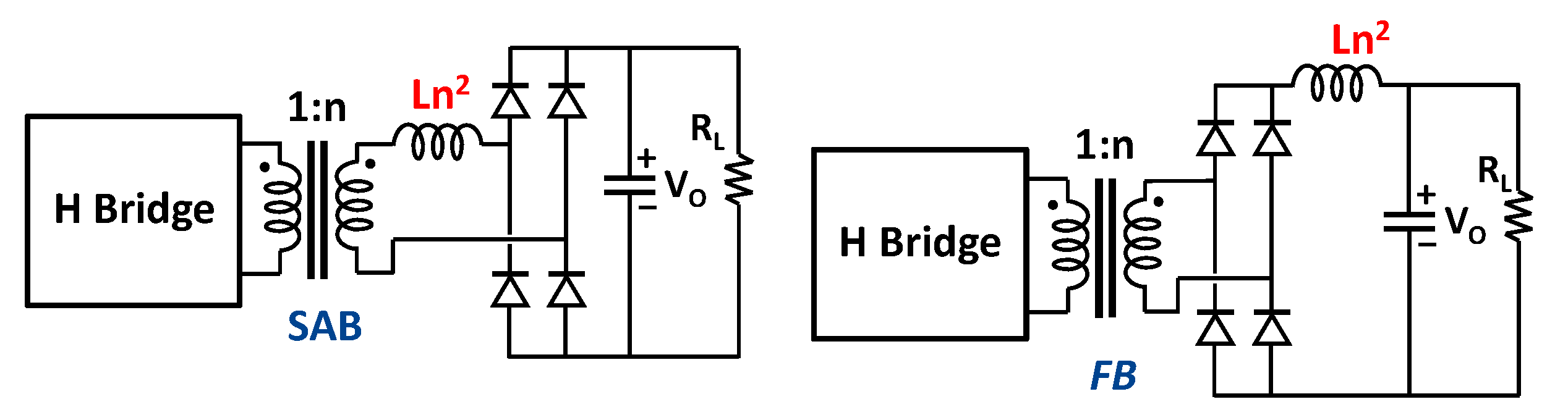
Therefore, if the power stages shown in
Figure 9 are compared, it can be concluded that the normalized voltage conversion ratio of both stages is the same if the stages have been designed to operate in DCM, whereas the normalized voltage conversion ratio of both stages differs completely if the stages start working in CCM. This also means that if the stages have been designed to operate in DCM, then the normalized voltage conversion ratio is independent of the position of the inductor, either before or after the output rectifier bridge. It should be noted that the position of the inductor modifies the maximum voltage withstood by the output diodes.
In
Table 1, the voltage conversion ratio in DCM of the previously described converters is shown to summarize the comparison of SAB with similar converters.
7. Converter Design Guide
The initial variables for the converter design, which are a function of the specifications of the application, are as follows:
- ▪
Maximum input voltage, Vgmax.
- ▪
Minimum input voltage, Vgmin.
- ▪
Maximum output voltage, Vomax.
- ▪
Minimum output voltage, Vomin.
- ▪
Maximum output current, Iomax.
- ▪
Minimum output current, Iomin.
- ▪
Maximum duty cycle, dmax, always lower than 0.5.
- ▪
Switching frequency, f.
Since the converter has a transformer, a certain voltage conversion ratio
VO/
Vg can be given by infinite possible values of
N, depending on the choice of
n and always taking into account (27). Moreover,
N depends on d and the choice of
L through
k. Therefore, a certain operation point, defined by
VO,
Vg, and
RL, can be achieved with infinite sets of values of
n,
d, and
L. That operation point will change during the use of the converter and the new operation point must be reached by changing only the value of d and always complying with the existing restrictions to the possible values of
d and
N (i.e.,
d <
dmax = 0.5 and
N <
Nmax = 1). Despite this, there are infinite combinations of n and L compatible with the new operation point obtained by changing
d. In conclusion, there is always a degree of freedom in the choice of
n and
L. Therefore, one of these values can be defined according to a certain objective. In this paper, an objective is proposed that the converter operates in CCM in a certain operating range. To do this, the value of
dcrit is set to the minimum input voltage and the maximum output voltage. This value of
dcrit is called
dcritmax. By setting this value, the value of
n is calculated from Equation (26), resulting in:
Once the value of n is chosen, the value of
L must be low enough to allow the converter to process the maximum output current, i.e., at
VOmax,
Vgmin, and
RLmin. Considering that
IOmax =
VOmax/
RLmin and using (19) and (20), the value of
L is obtained with:
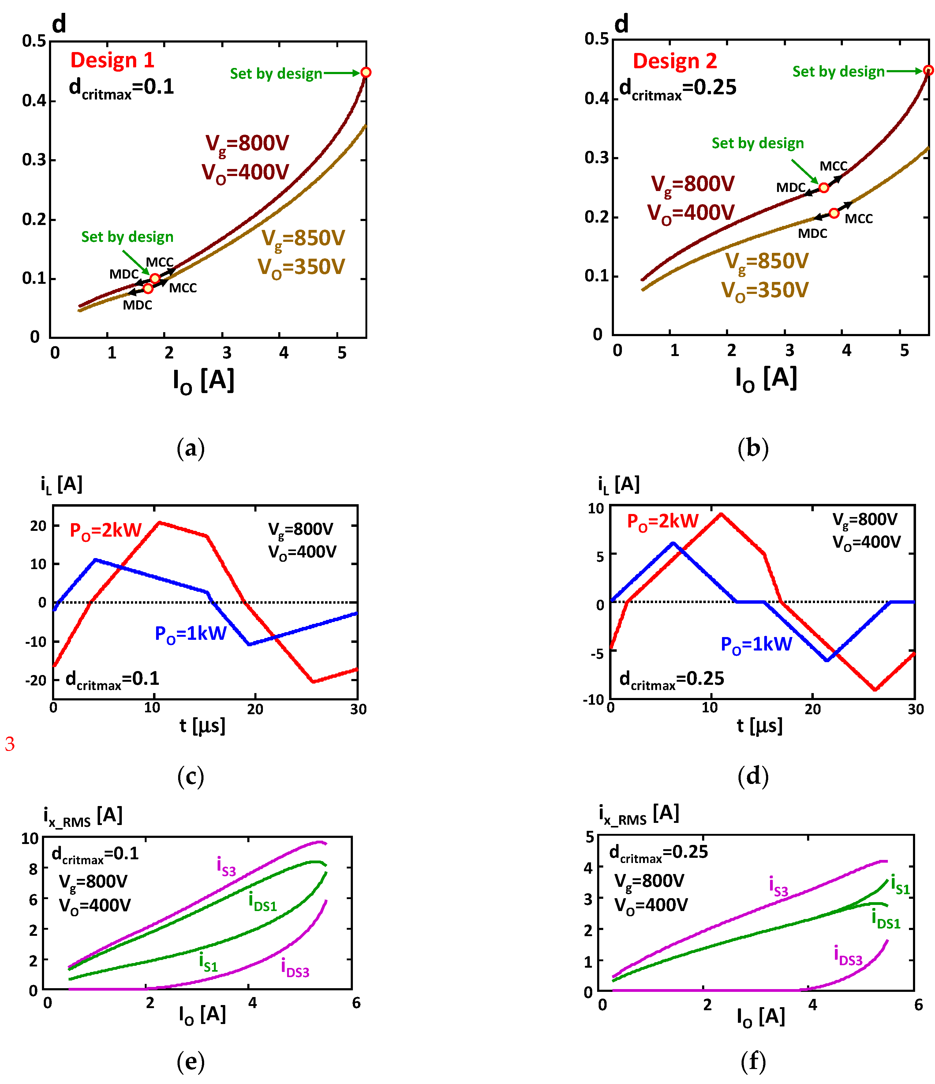
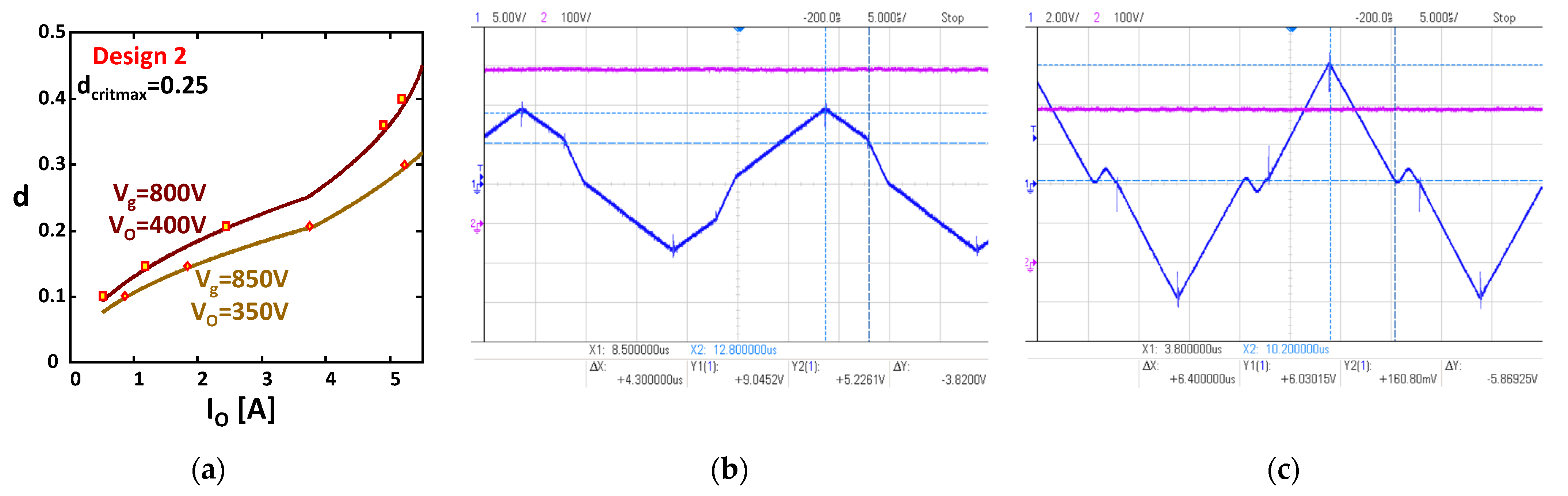
Two different design examples are shown here. The following specifications are the same for both designs: Vgmax = 850 V; Vgmin = 800 V; Vomax = 400 V; Vomin = 350 V; Iomax = 5.5 A; Iomin = 0.5 A; dmax =0.45; f = 33 kHz. The difference between the two designs is the selection of dcritmax:
Design1: dcritmax = 0.1 is selected. With the previously described global specifications, n is calculated using (59), obtaining the value of n = 2.5. With the previously calculated value of n and the global specifications, L is calculated using (60), obtaining the value of L = 209 µH.
Design2: dcritmax = 0.25 is selected. With the previously described global specifications, n is calculated using (59), obtaining the value of n = 1. With the previously calculated value of n and the global specifications, L is calculated using (60), obtaining the value of L = 408 µH.
In
Figure 10a,b, the evolution of the duty cycle depending on the output current is shown when the converter works in closed loop for both designs. These curves are obtained as in
Figure 6b, i.e., from Equations (19) and (23) and by clearing the value of d in them. The difference is that the independent variable is in this case
IO =
VO/
RL instead of
RL. It can be observed that choosing
dcritmax = 0.1 (Design 1), the converter operates in CCM for most of the I
O variation range. This is attractive for reducing switching losses, but it penalizes conduction losses. In Design 2 (
dcritmax = 0.25), since the converter works in DCM for most
IO values, conduction losses are reduced while switching losses are penalized. In
Figure 10c,d, the waveforms corresponding to
VO = 400 V,
Vg = 800 V and two output power levels are shown. Comparing the two figures, the current values in the second design are lower than in the first. The same pattern can be seen in more detail in
Figure 10e,f, which show the rms values of the current passing through the transistors and anti-parallel diodes of the leading branch (taking as an example S
3 and DS
3) and the lagging branch (taking as an example S
1 and DS
1). Considering the scales of the figures it is clear the conduction losses are lower in the second design.
8. Simulation and Experimental Results
The verification of the proposed static analysis of the SAB converter was initially carried out by simulation with PSIM on a converter with ideal components and the same characteristics as those presented in the design examples. The results predicted by the theory perfectly matched the results at various simulated operating points. In addition, the waveforms obtained in the simulation perfectly matched those produced by the theory. Simulation results are not shown because they are the same as the presented analytical results.
A preliminary SAB prototype has been developed and tested to validate the analytical study proposed in this paper. The prototype has the characteristics of Design 2. Experimental (squares and diamonds) and analytical (continuous line) results at various operating points are compared in
Figure 11a with good agreement. Moreover, experimental waveforms obtained using the prototype and shown in
Figure 11b,c match those obtained from the theory (
Figure 10d). As can be seen in
Figure 11c, a small resonant period is observed during the intervals where the inductor current should theoretically be zero. This resonant period is caused by the reverse recovery current of the anti-parallel diodes of the main transistors. This phenomenon occurs on many occasions when DC/DC converters work in DCM.
9. Conclusions
In this paper, the static behavior of the SAB converter has been thoroughly studied. The voltage conversion ratio in both CCM and DCM have been found, as well as the conditions for the change of conduction mode. Unlike other converters, operation in CCM does not imply low open loop output impedance, but, as in DCM, this converter has a high output impedance under both conduction modes. This means that when the converter works in a closed loop, its duty cycle changes extensively when changing the load in both conduction modes. It is also appreciated that the design for operation in CCM reduces switching losses, but penalizes conduction losses, just the opposite of operating in DCM. Finally, operation in DCM is identical to that of buck, forward and phase shifted full-bridge converters if appropriate transformations related to the switching frequency, duty cycle, and inductance value are performed.


 ,
, 


