Abstract
An acoustic second-order low-pass filter is proposed for filter banks emulating the operation of a human cochlea. By using a special filter structure and an innovative quality (Q)-factor tuning technique, an independent change of the cutoff frequency (ω0) and the Q-factor with unchanged gain at low frequencies is achieved in this filter. The techniques applied result in a simple filter design with low Q-factor sensitivity to component mismatch. These filter features greatly simplify the implementation of the electronic cochlea in CMOS technologies. An exemplary filter bank designed and simulated in an X-FAB 180 nm CMOS process is presented, which consumes 1.25–34.75 nW of power per individual filter when supplied with 0.5 V. The 11-channel filter bank covers a 20–20 kHz band, while the Q-factor of each channel can be tuned from 2 to 40. The simulation-predicted sensitivities of Q and ω0 to process/voltage/temperature (PVT) variations are less than 1%. The input-referred noise is no greater than 22 µVRMS, and the dynamic range is at least 68 dB for all filters in the bank.
1. Introduction
Systems for effective human speech processing and recognition are of increasing practical importance. They are used in controlling machines with the human voice [1], as well as in hearing aids [2,3,4,5,6]. Electronic circuits that emulate the operation of a human cochlea are gaining interest in such applications. The popularity of this approach comes from the belief that millions of years of evolution have led to a solution that is optimally suited for processing human speech in typical human environments. Work conducted on the physiology of hearing, particularly on the functioning of the cochlea, has enabled understanding the operation of this very important organ of the inner ear [7,8,9]. Due to the special properties of the cochlea, humans are able to hear and understand quiet speech even in environments with disruptive sounds. This highly desirable feature of human hearing is related to the ability of the cochlea to analyze and dynamically adjust to the properties of the sound heard. The cochlea processes the pressure of the received acoustic wave in multiple paths. Thus, the operation of the cochlea is similar to the operation of a system with multiple bandpass channels whose sensitivity is dynamically tuned to the volume of the sound, whereas out-of-band frequency components are largely suppressed. An accurate, complex model of the cochlea [10,11] takes into account both the processing of acoustic signals in individual channels and the coupling between the channels. However, due to practical limitations in electronic VLSI (very-large-scale integration) cochlea implementations, filter banks emulating only bandpass channels without coupling are most often used as compromise solutions [12,13,14,15,16,17,18]. Two architectures of the filter banks are used, consisting of elementary sections connected in cascade [12,13,14,15] or in parallel [16,17,18]. In both architectures, the key and difficult-to-implement feature is the low-pass biquadratic filter section with electronically programmable cutoff frequency and quality factor. For precise signal processing, the frequency characteristics of biquadratic sections should be insensitive to process/voltage/temperature (PVT) variations.
A number of publications have been devoted to the design of filters intended for electronic cochlea. The earliest developed solutions [10,11,12,13,14] feature relatively high power consumption and supply voltage; therefore, they cannot be used in implants or systems with limited power supply (powered by small batteries). In addition, some of these solutions [12,13] do not provide sufficient accuracy in signal processing, which is limited by the influence of circuit parameter variations.
This paper proposes a new filter solution well suited to the requirements of an electronic cochlea powered by a small battery or small renewable energy source based on, e.g., thermoelectric generators or electromagnetic energy harvesters. By using a “transistorized” filter structure with transistors operating in the sub-threshold range [19], a significant reduction in voltage and power supply was achieved. As a result of the special tuning method of the filter quality factor and other applied techniques, a high robustness to PVT variations was obtained.
2. Proposed Filter Solution
2.1. Principle of Operation
The transfer function of the second-order low-pass filter (biquadratic) expressed in the Laplace domain is as follows:
where Vout and Vin are the output and input voltages of the filter, A in V/V is the gain of the filter at zero frequency (DC gain), ω0 in rad/s is the natural frequency (ω0 = 2πf0), and QLP (dimensionless) denotes a quality factor.
Figure 1 shows a family of plots of the amplitude characteristics, |H(jω)| versus ω, for three exemplary values of QLP. The plots are normalized for ω0 of 1 rad/s, and A is assumed to be 1 V/V.
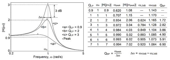
Figure 1.
A family of plots of the amplitude characteristics for different QLP (A = 1) and detailed numerical data on the plot parameters.
The bulged portion of the characteristic around ω0 can be used for bandpass filtering if QLP is at least 2. In this case (QLP ≥ 2), ω0 and QLP can be treated as a center (or peak-gain) frequency and as a quality factor of a bandpass filter, i.e., ωcenter (or ωpeak) and QBP. The detailed numerical data show that ω0 is practically equal to ωpeak (ω0 ≅ ωpeak) if QLP is at least 2. The factor QBP is approximately equal to QLP (QBP ≈ QLP) when QLP is 2–4, and QBP is practically equal to QLP (QBP ≅ QLP) if QLP is 5 or more.
This particular shape of the characteristics allows this filter to emulate the basic properties of the cochlea in the human ear. By using an appropriate set of such filters, the functioning of the human inner ear can be imitated faithfully enough [12,13,14,15,16,17,18]. Electronic emulation of the cochlea uses filter banks in which each filter emulates particular resonant property of this organ. In simple terms, adaptation of the electronic cochlea to different sound levels involves splitting the sound spectrum into a number of channels with different center (peak-gain) frequencies, and then adjusting the gain in each channel individually. In channels where the sound strength is low, the filter gain is increased, and, in channels where the sound strength is high, the gain is reduced accordingly to achieve the most effective sound processing. To faithfully represent the physiological properties of the cochlea, the gain in the passband of each filter must be adjusted to mimic the ear’s ability to adapt to different sound levels. This capability can be achieved by tuning the quality factor QLP of the low-pass filter since the value of this factor determines the value of the filter peak gain, as shown in Figure 1 (|H(jωpeak)| ≈ QLP for QLP < 2, |H(jωpeak)| ≅ QLP for QLP ≥ 2).
Figure 2 shows a proposed filter that has the desirable feature of tuning the QLP-factor by changing the attenuation (kQ). The filter consists of two transconductance amplifiers (Gm1, Gm2), two capacitors (C1, C2), and one attenuator (kQ).
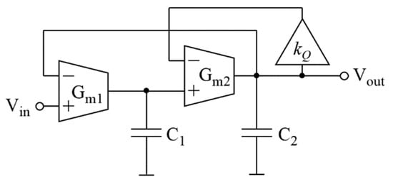
Figure 2.
Proposed second-order low-pass filter with independent QLP-factor tuning (OTA-C structure).
The filter in Figure 2 has the transmittance in Equation (1), in which A, ω0 and QLP are
where kQ is the voltage gain (in V/V) of the attenuator. Thus, kQ is assumed to be smaller than 1. All the undefined parameters have their usual meaning. The proposed high-Q filter structure with tunable Q is an extended version of the low-Q and not tunable structure presented in [19].
2.2. Sensitivity
In electronic cochlea emulators, banks consisting of many filters with center (peak-gain) frequencies of little difference are often used. In such solutions, it is particularly important to ensure that the peak gain frequencies and the peak gain magnitudes of the individual filters are sufficiently precise. The accuracy of filters implemented in CMOS technologies is influenced by the PVT variations. For the proposed filter in Figure 2, the influence of these factors on the peak gain frequency (≅ω0) and the peak gain magnitude (≅QLP) can be determined according to the following sensitivities:
where Gm1/Gm2 = kG12, and C2/C1 = kC21.
While determining the sensitivities, the peak gain frequency ω0 is assumed to be tuned by a simultaneous change of the transconductances Gm1, Gm2 or capacitances C1, C2 such that their ratio Gm1/Gm2 (or C2/C1) is constant and, thus, QLP remains unchanged. However, because of technology nonidealities, these ratios may vary, especially if an ω0 tuning range is wide. Notice that the sensitivities in Equations (3) and (4) are relatively small (≤1) and do not depend on the value of QLP. This means that the inaccuracy of ω0 and QLP does not exceed the inaccuracy of the parameters of the technology itself, which is a very advantageous feature of this filter structure. For example, a 1% variation in the transconductance ratio kG12 due to a technology imperfection induces only a 0.5% change in peak gain magnitude. Moreover, a high value of the peak gain magnitude can be obtained at low values of the transconductance and capacitance ratios, e.g., with kG12 and kC21 in the range of 1–2. Due to this, transconductors and capacitors of similar parameter values (unit components) can be used in the filter, which allows for an even better matching of these components, thereby obtaining a much better accuracy of ω0 and QLP realization. In addition, the use of the unit components significantly simplifies the filter design.
2.3. Noise
The filter noise performance can be analyzed according to the schematic in Figure 3, in which the equivalent (input-referred) noise sources for each amplifier are introduced.
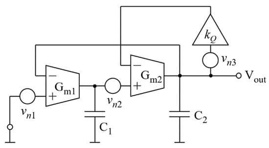
Figure 3.
Schematic for noise analysis.
Assuming that the noise sources are characterized by the power spectral densities, , , and , the respective powers of noise at the filter output are
Thus, the total noise power spectral density, referred to the filter input, is
It can be deduced from Equation (5) that the noise sources of the second transconductance amplifier and the voltage attenuator, vn2 and vn3, are shaped identically due to the same factor of ωC1/Gm1. However, the attenuator’s noise is reduced further due to the factor of kQ (kQ is smaller than 1). As a result, the attenuator does not substantially degrade the filter noise performance.
2.4. Transistor-Level Circuit
The transistor-level implementation of the OTA-C structure of Figure 2 is shown in Figure 4. The operational transconductance amplifiers (OTAs) are composed of the transistors M1–M4 and 2 × M0. The additional transistors MSH1, MSH2 are DC voltage shifters which improve the operating point conditions for OTAs [19]. All the transistors operate in the saturated subthreshold (weak inversion) region. The transconductances of OTAs are assumed to be identical, i.e., Gm1 = Gm2 = Iω/(np∙UT) (np is the subthreshold slope factor for p-channel transistors, UT is the thermal voltage, UT = k∙T/q). The filter capacitances are also assumed to be identical, C1 = C2. By using the floating capacitors (C1/2, C2/2), a twofold reduction in total capacitance and, thus, the area occupied by the filter was achieved [19].
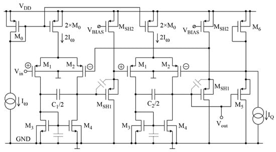
Figure 4.
Transistor-level implementation of the filter in Figure 2.
The attenuator consists of transistors M5–M6 and the current source IQ. Its gain depends on the transconductance of the transistors M5 and M6, i.e., kQ = gm5/(gm5 + gm6). For IQ equal to zero, both transistors M5 and M6 conduct the same current; therefore, gm6 = gm5, and kQ = 1/2. Increasing IQ makes the current flowing through M6 larger than that through M5; as a result, kQ decreases, according to the following formula:
where Iq is a quiescent (DC) current flowing through M5 and M6 when IQ is zero.
For the filter in Figure 4, the transmittance parameters can be tuned independently by the currents Iω and IQ, as explained by Equation (7) and the following formulas:
where Gm1 = Gm2, C1 = C2, and kQ ≤ 1/2 are assumed.
For the assumed kQ ≤ 1/2 (QLP ≥ 2), ω0 is practically equal to ωpeak, while QLP is well correlated with the peak gain magnitude and QBP, as explained in Section 2.1; thus, the designed filter satisfies the following equations:
3. Filter Bank
An exemplary set of 11 filters was designed to cover the full audio band from 20 Hz to 20 kHz. Thus, the peak-gain frequencies fpeak (fpeak = ωpeak/2/π) of the consecutive filters form an octave series, i.e., 20, 40, 80, …, 10,240, and 20,480 Hz. The transistor sizes (in µm/µm) in all filters are M0 = 10/6, M1 = M2 = 8/2, M3 = M4 = 10/10, M5 = M6 = 2/2, MSH1 = 30/3, MSH2 = 10/6. The bias current flowing through transistors MSH1–MSH2 is 0.25 nA. The values of the current setting the filter frequencies and the capacitances used in each filter are specified in Table 1.

Table 1.
Simulated 1 post-layout parameters of the individual filters with VDD = 0.5 V.
Figure 5 presents the amplitude characteristics of the filter bank for different values of parameter kQ, i.e., for different target peak gain values. The gain nonuniformity of the filter bank is relatively small, with differences between the peak gains of individual filters of ±0.5 dB for low gains and ±1 dB for high gains. The DC gain is 0 dB in all filters (A = 1). Note also that all filters feature a high stop-band attenuation of at least 50 dB.
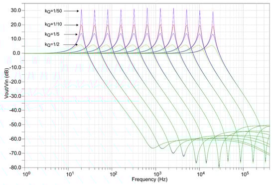
Figure 5.
Amplitude responses of the filter bank simulated using nominal device models.
The detailed values of the obtained peak gain magnitude, peak gain frequency fpeak, and values of the factor QBP are in Figure 6a–c. These figures show zoomed-in passband portions of the amplitude characteristics for the three selected filters: for the lowest (20 Hz), middle (1.28 kHz), and highest (20.48 kHz) frequencies, respectively.
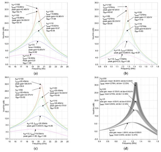
Figure 6.
Simulated amplitude responses of the selected filters: (a–c) 20 Hz, 1.28 kHz, and 20.48 kHz filters (nominal simulation); (d) 1.28 kHz filter under technology mismatch (500 Monte Carlo simulation runs).
In Figure 6a–c, it can be seen that, for small and medium values, the peak gain of the filters is approximately equal to QBP (QBP ≈ peak gain), which is consistent with the theory illustrated in Figure 1. However, at large values of the peak gain, the Q tuning process becomes nonlinear, i.e., the peak gain is no longer directly proportional to 1/kQ as shown in Equation (9). For example, in Figure 6b, the peak gain is 17.5 V/V for kQ of 1/20 V/V, and the peak gain is 38 when kQ is 1/50. This is caused by finite output resistance of OTAs (0.3–1.5 GΩ) which limits the maximum peak gain to 50–55 V/V. The tuning of the peak gain frequency is performed according to Equation (9), i.e., ωpeak ≅ ω0. The results in Figure 6a–c show that, when the quality factor increases, ωpeak (fpeak) moves from left to right, approaching the target value of ω0 (f0) (which is consistent with the theory in Figure 1). Details of the obtained fpeak values are also given in Table 1.
Simulations which take into account technology parameter variation and component mismatch show that the peak-gain-magnitude and peak-gain-frequency variations are less than 1% (1 sigma) for all filters in the bank. Exemplary Monte Carlo simulation results for the middle-band 1.28-kHz filter are shown in Figure 6d. Details of this filter’s performance under PVT variations are provided in the Appendix A.
All the filters feature a maximum amplitude of the input sinusoidal signal of at least 86 mVpeak at 1% output THD (fundamental frequency = f0/10). The input-referred noise integrated from 1 Hz to 2f0 is less than 22 µVRMS for all the filters, resulting in a filter bank dynamic range of 68 dB.
4. Discussion
The filter shown in Figure 7 is often used in many practical implementations of an electronic cochlea [12,13,14,15,20]. Therefore, this section compares the key features of this filter, which has become the preferred solution in the cochlea, with the features of the proposed new filter structure shown in Figure 2.
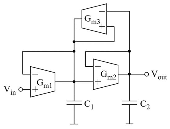
Figure 7.
Structure of a second-order low-pass filter frequently used in electronic cochlea implementations.
The filter in Figure 7 has the transmittance in Equation (1) with the following parameters:
The frequency ω0 can be tuned in the same manner as in the proposed filter, shown in Figure 2, by changing Gm1, Gm2 or C1, C2. To achieve ω0 tuning independent of QLP, it is necessary to keep constant values of the transconductance Gm1/Gm2 and capacitance C1/C2 ratios. Under these conditions, QLP tuning requires changing the transconductance of the positive-feedback-connected amplifier (Gm3). With these assumptions, the sensitivities of QLP to variations in transconductance and capacitance ratios are
where kG12 and kC21 are defined in Equation (4), and kG32 = Gm3/Gm2.
For a practical design case, i.e., kG12 = kC21 = 1, the quality factor is QLP = 1/(2 − kG32), and Equation (10) becomes
Comparing Equations (3) and (11), defining the sensitivities of the compared filters, it can be observed that, for all practical cases when QLP ≥ 2, the proposed filter has a much lower sensitivity to implementation mismatch between the transconductors (Gm1, Gm2) and the capacitors (C1, C2). Thus, the proposed filter is better suited for practical implementation in CMOS technologies.
5. Comparison to the State of the Art and Conclusions
Requirements for the filter banks used in electronic cochlea implementation depend on their application. In systems designed to control machines with the human voice, the values of the supply voltage and power consumption are usually less important, whereas the precision of the frequency characteristics is crucial. The most difficult criteria to meet are those related to hearing aid implants and devices for Internet of things. In such cases, low supply voltage and low power consumption must additionally be ensured due to the fact that such devices are powered from small batteries or small renewable energy sources based on, e.g., thermoelectric generators or electromagnetic energy harvesters. Therefore, in the presented comparison of the filter banks reported in the literature (Table 2), special attention was paid to these critical parameters.
Table 2.
Performance comparison of filter banks designed for electronic cochlea.
In the proposed filter bank, similarly to the implementation in [18], a relatively low supply voltage of 0.5 V was used, which allowed a reduction in power consumption. Note that, in [18], an additional programmable gain amplifier was required for proper operation of the filter, whose power supply is not included in the data in Table 1. Having this fact in mind, it can be concluded that the proposed solution is more beneficial in terms of power consumption. In practical implementation of the filters in CMOS technology, an important problem is to obtain a low sensitivity of the center frequency f0 and the quality (Q) factor to PVT variations. This issue is particularly important in systems with a large number of channels [15,17,18], where the center frequencies of consecutive channels do not differ much. For this reason, a special adjustment system is used in the implementation [15]. Such a solution complicates the whole system, increasing its area and power consumption. The data in Table 2 show that the variation of f0 and Q in the proposed filter bank is smaller compared to the other solutions. Another very critical problem in the solution proposed in [18] is a quadratic dependence of the filter gain at low frequencies on the Q-factor value. The consequence of such a dependence is a reduction in signal dynamics. This reduction results from the fact that, e.g., a fivefold increase in the filter Q-factor leads to a 25-fold increase in the filter gain and, consequently, the output signal amplitude. To reduce the impact of this phenomenon, additional attenuators at the filter input were applied in [18]. As can be seen from Equations (1) and (2), the proposed filter is free from this unfavorable feature because the low-frequency (DC) gain is always equal to one (A = 1).
Author Contributions
All authors contributed equally to conceptualization, methodology, formal analysis, simulations, writing—original draft preparation, and writing—review and editing. All authors have read and agreed to the published version of the manuscript.
Funding
This research was funded in part by the National Science Centre of Poland under grant 2016/23/B/ST7/03733.
Conflicts of Interest
The authors declare no conflict of interest.
Appendix A
This appendix provides, in Table A1, Table A2 and Table A3, simulation results of the proposed filter performance under PVT variations (process: CMOS X-FAB 180 nm xh018).
Table A1.
Corner simulation results for the middle-band filter at VDD of 0.5 V.
Table A1.
Corner simulation results for the middle-band filter at VDD of 0.5 V.
| T = 0 °C | T = 27 °C | T = 50 °C | |||||||||||||
|---|---|---|---|---|---|---|---|---|---|---|---|---|---|---|---|
| kQ | TM | WP | WS | WO | WZ | TM | WP | WS | WO | WZ | TM | WP | WS | WO | WZ |
| fpeak (Hz) | |||||||||||||||
| 1/50 | 1360 | 1395 | 1313 | 1326 | 1380 | 1281 | 1312 | 1246 | 1259 | 1298 | 1211 | 1241 | 1176 | 1187 | 1228 |
| 1/10 | 1357 | 1393 | 1309 | 1323 | 1378 | 1279 | 1310 | 1244 | 1256 | 1296 | 1208 | 1239 | 1173 | 1185 | 1226 |
| 1/5 | 1349 | 1385 | 1299 | 1312 | 1370 | 1271 | 1302 | 1235 | 1247 | 1288 | 1200 | 1231 | 1165 | 1177 | 1218 |
| 1/2 | 1274 | 1309 | 1221 | 1233 | 1295 | 1201 | 1231 | 1165 | 1177 | 1218 | 1134 | 1163 | 1099 | 1109 | 1152 |
| peak gain (V/V) | |||||||||||||||
| 1/50 | 43.47 | 69.35 | 18.34 | 18.08 | 68.44 | 70.29 | 79.3 | 43.9 | 43.59 | 77.25 | 76.53 | 53.82 | 66.47 | 66.69 | 51.48 |
| 1/10 | 10.13 | 11.11 | 7.658 | 7.62 | 11.04 | 11.11 | 11.35 | 10.11 | 10.11 | 11.24 | 11.24 | 10.65 | 10.93 | 10.95 | 10.49 |
| 1/5 | 5.15 | 5.4 | 4.421 | 4.41 | 5.367 | 5.39 | 5.456 | 5.137 | 5.14 | 5.413 | 5.42 | 5.296 | 5.325 | 5.34 | 5.238 |
| 1/2 | 2.03 | 2.067 | 1.907 | 1.91 | 2.055 | 2.06 | 2.076 | 2.023 | 2.03 | 2.061 | 2.07 | 2.056 | 2.047 | 2.05 | 2.039 |
| DC gain (V/V) | |||||||||||||||
| 1/50 | 0.9988 | 0.9992 | 0.998 | 0.9989 | 0.9956 | 0.9991 | 0.9999 | 0.9985 | 0.9996 | 0.9957 | 0.9997 | 1.003 | 0.9987 | 0.9999 | 0.9979 |
| 1/10 | 0.9979 | 0.9986 | 0.9961 | 0.9970 | 0.995 | 0.9984 | 0.9994 | 0.9976 | 0.9987 | 0.9951 | 0.9991 | 1.002 | 0.998 | 0.9992 | 0.9971 |
| 1/5 | 0.9968 | 0.9978 | 0.9938 | 0.9947 | 0.9942 | 0.9977 | 0.9986 | 0.9965 | 0.9976 | 0.9943 | 0.9983 | 1.001 | 0.9972 | 0.9984 | 0.996 |
| 1/2 | 0.9932 | 0.9953 | 0.9862 | 0.9871 | 0.9917 | 0.9951 | 0.9962 | 0.9929 | 0.9940 | 0.9919 | 0.9958 | 0.9974 | 0.9945 | 0.9957 | 0.9925 |
Table A2.
Corner simulation results for the middle-band filter at VDD of 0.475 V.
Table A2.
Corner simulation results for the middle-band filter at VDD of 0.475 V.
| T = 0 °C | T = 27 °C | T = 50 °C | |||||||||||||
|---|---|---|---|---|---|---|---|---|---|---|---|---|---|---|---|
| kQ | TM | WP | WS | WO | WZ | TM | WP | WS | WO | WZ | TM | WP | WS | WO | WZ |
| fpeak (Hz) | |||||||||||||||
| 1/50 | 1354 | 1392 | 1294 | 1307 | 1377 | 1279 | 1311 | 1243 | 1255 | 1297 | 1211 | 1241 | 1177 | 1189 | 1228 |
| 1/10 | 1351 | 1390 | 1289 | 1302 | 1375 | 1277 | 1309 | 1240 | 1252 | 1295 | 1209 | 1239 | 1174 | 1186 | 1226 |
| 1/5 | 1342 | 1381 | 1277 | 1290 | 1366 | 1269 | 1300 | 1231 | 1244 | 1287 | 1201 | 1231 | 1166 | 1178 | 1219 |
| 1/2 | 1266 | 1306 | 1194 | 1206 | 1291 | 1199 | 1230 | 1160 | 1171 | 1217 | 1135 | 1164 | 1100 | 1111 | 1152 |
| peak gain (V/V) | |||||||||||||||
| 1/50 | 32.3 | 58.25 | 11.35 | 11.15 | 57.58 | 58.79 | 72.47 | 32.57 | 32.22 | 70.68 | 69.53 | 53.11 | 54.71 | 54.61 | 50.81 |
| 1/10 | 9.364 | 10.78 | 6.081 | 6.03 | 10.69 | 10.77 | 11.19 | 9.356 | 9.34 | 11.06 | 11.08 | 10.62 | 10.56 | 10.58 | 10.44 |
| 1/5 | 4.945 | 5.318 | 3.842 | 3.83 | 5.275 | 5.311 | 5.419 | 4.933 | 4.94 | 5.363 | 5.38 | 5.288 | 5.238 | 5.25 | 5.216 |
| 1/2 | 1.996 | 2.055 | 1.792 | 1.79 | 2.039 | 2.052 | 2.07 | 1.991 | 1.99 | 2.05 | 2.061 | 2.055 | 2.035 | 2.04 | 2.031 |
| DC gain (V/V) | |||||||||||||||
| 1/50 | 0.9984 | 0.9989 | 0.9967 | 0.9978 | 0.994 | 0.9987 | 0.9996 | 0.9980 | 0.9994 | 0.9937 | 0.9993 | 1.002 | 0.9982 | 0.9998 | 0.9955 |
| 1/10 | 0.9973 | 0.9982 | 0.9938 | 0.9949 | 0.9933 | 0.998 | 0.999 | 0.9969 | 0.9983 | 0.9931 | 0.9987 | 1.001 | 0.9975 | 0.9990 | 0.9946 |
| 1/5 | 0.9959 | 0.9974 | 0.9901 | 0.9911 | 0.9924 | 0.9971 | 0.9982 | 0.9955 | 0.9969 | 0.9923 | 0.9979 | 1 | 0.9966 | 0.9981 | 0.9936 |
| 1/2 | 0.9913 | 0.9945 | 0.9782 | 0.9792 | 0.9895 | 0.9942 | 0.9957 | 0.9910 | 0.9923 | 0.9897 | 0.9952 | 0.9969 | 0.9935 | 0.9950 | 0.9901 |
Table A3.
Corner simulation results for the middle-band filter at VDD of 0.525 V.
Table A3.
Corner simulation results for the middle-band filter at VDD of 0.525 V.
| T = 0 °C | T = 27 °C | T = 50 °C | |||||||||||||
|---|---|---|---|---|---|---|---|---|---|---|---|---|---|---|---|
| kQ | TM | WP | WS | WO | WZ | TM | WP | WS | WO | WZ | TM | WP | WS | WO | WZ |
| fpeak (Hz) | |||||||||||||||
| 1/50 | 1364 | 1397 | 1323 | 1338 | 1383 | 1282 | 1313 | 1247 | 1260 | 1299 | 1209 | 1240 | 1172 | 1184 | 1227 |
| 1/10 | 1361 | 1395 | 1320 | 1335 | 1380 | 1279 | 1310 | 1245 | 1258 | 1297 | 1206 | 1238 | 1169 | 1181 | 1226 |
| 1/5 | 1353 | 1387 | 1311 | 1324 | 1372 | 1272 | 1302 | 1237 | 1249 | 1289 | 1199 | 1230 | 1161 | 1173 | 1218 |
| 1/2 | 1278 | 1312 | 1235 | 1248 | 1298 | 1202 | 1232 | 1167 | 1179 | 1219 | 1132 | 1162 | 1095 | 1106 | 1151 |
| peak gain (V/V) | |||||||||||||||
| 1/50 | 55.63 | 79.94 | 27.41 | 27.11 | 78.8 | 81.4 | 84.94 | 56.47 | 56.28 | 82.8 | 82.45 | 53.81 | 78.38 | 78.87 | 51.44 |
| 1/10 | 10.68 | 11.36 | 8.897 | 8.87 | 11.3 | 11.36 | 11.46 | 10.66 | 10.67 | 11.37 | 11.35 | 10.65 | 11.18 | 11.21 | 10.51 |
| 1/5 | 5.294 | 5.459 | 4.81 | 4.81 | 5.433 | 5.451 | 5.483 | 5.273 | 5.28 | 5.448 | 5.441 | 5.296 | 5.381 | 5.39 | 5.247 |
| 1/2 | 2.051 | 2.076 | 1.974 | 1.98 | 2.067 | 2.072 | 2.08 | 2.043 | 2.05 | 2.069 | 2.069 | 2.057 | 2.053 | 2.06 | 2.043 |
| DC gain (V/V) | |||||||||||||||
| 1/50 | 0.9991 | 0.9995 | 0.9986 | 0.9993 | 0.9968 | 0.9993 | 1 | 0.9988 | 0.9993 | 0.997 | 1 | 1.003 | 0.9990 | 1.0000 | 0.9997 |
| 1/10 | 0.9983 | 0.9989 | 0.9973 | 0.9980 | 0.9962 | 0.9988 | 0.9996 | 0.9981 | 0.9980 | 0.9965 | 0.9995 | 1.002 | 0.9985 | 0.9994 | 0.9988 |
| 1/5 | 0.9974 | 0.9982 | 0.9956 | 0.9964 | 0.9955 | 0.9981 | 0.9989 | 0.9972 | 0.9964 | 0.9958 | 0.9987 | 1.001 | 0.9977 | 0.9987 | 0.9977 |
| 1/2 | 0.9944 | 0.9958 | 0.9903 | 0.9911 | 0.9931 | 0.9957 | 0.9966 | 0.9942 | 0.9911 | 0.9934 | 0.9963 | 0.9978 | 0.9953 | 0.9962 | 0.9942 |
References
- Russo, M.; Stella, M.; Sikora, M.; Pekić, V. Robust Cochlear-Model-Based Speech Recognition. Computers 2019, 8, 5. [Google Scholar] [CrossRef]
- Raychowdhury, A.; Tokunaga, C.; Beltman, W.; Deisher, M.; Tschanz, J.W.; De, V. A 2.3 nJ/frame voice activity detector-based audio front-end for context-aware system-on-chip applications in 32-nm CMOS. IEEE J. Solid-State Circuits 2013, 48, 1963–1969. [Google Scholar] [CrossRef]
- Price, M.; Glass, J.; Chandrakasan, A.P. A 6 mW, 5000-word real-time speech recognizer using WFST models. IEEE J. Solid-State Circuits 2015, 50, 102–112. [Google Scholar] [CrossRef]
- Yang, G.; Lyon, R.F.; Drakakis, E.M. A 6 μW per channel analog biomimetic cochlear implant processor filterbank architecture with across channels AGC. IEEE Trans. Biomed. Circuits Syst. 2015, 9, 72–86. [Google Scholar] [CrossRef] [PubMed]
- Harczos, T.; Chilian, A.; Husar, P. Making use of auditory models for better mimicking of normal hearing processes with cochlear implants: The SAM coding strategy. IEEE Trans. Biomed. Circuits Syst. 2013, 7, 414–425. [Google Scholar] [CrossRef] [PubMed]
- Yip, M.; Jin, R.; Nakajima, H.H.; Stankovic, K.M.; Chandrakasan, A.P. A Fully-Implantable Cochlear Implant SoC With Piezoelectric Middle-Ear Sensor and Arbitrary Waveform Neural Stimulation. IEEE J. Solid-State Circuits 2015, 50, 214–229. [Google Scholar] [CrossRef] [PubMed]
- Robles, L.; Ruggero, M.A.; Rich, N.C. Mössbauer measurements of the mechanical response to single-tone and two-tone stimuli at the base of of the chinchilla cochlea. In Peripheral Auditory Mechanisms; Allen, J.B., Hall, J.L., Hubbard, A., Neely, S.T., Tubis, A., Eds.; Springer: Berlin/Heidelberg, Germany, 1986; pp. 121–128. [Google Scholar] [CrossRef]
- Ruggero, M.A.; Narayan, S.S.; Temchin, A.N.; Recio, A. Mechanical bases of frequency tuning and neural excitation at the base of the cochlea: Comparison of basilar-membrane vibrations and auditory-nerve-fiber responses in chinchilla. Proc. Natl. Acad. Sci. USA 2000, 97, 11744–11750. [Google Scholar] [CrossRef] [PubMed]
- Plack, C.J. The Sense of Hearing; Lawrence Erlbaum Associates: Mahwah, NJ, USA, 2005; ISBN 0805848843/9780805848847. [Google Scholar]
- Hamilton, T.J.; Jin, C.; van Schaik, A.; Tapson, J. An active 2-D silicon cochlea. IEEE Trans. Biomed. Circuits Syst. 2008, 2, 30–43. [Google Scholar] [CrossRef] [PubMed]
- Wen, B.; Boahen, K. A silicon cochlea with active coupling. IEEE Trans. Biomed. Circuits Syst. 2009, 3, 444–455. [Google Scholar] [CrossRef]
- Lyon, R.F.; Mead, C. An analog electronic cochlea. IEEE Trans. Acoust., Speech Signal Process. 1988, 36, 1119–1134. [Google Scholar] [CrossRef]
- Watts, L.; Kerns, D.A.; Lyon, R.F.; Mead, C.A. Improved implementation of the silicon cochlea. IEEE J. Solid-State Circuits 1992, 27, 692–700. [Google Scholar] [CrossRef]
- Sarpeshkar, R.; Lyon, R.F.; Mead, C.A. An analog VLSI cochlea with new transconductance amplifiers and nonlinear gain control. In Proceedings of the 1996 IEEE International Symposium on Circuits and Systems. Circuits and Systems Connecting the World. ISCAS 96, Atlanta, GA, USA, 15 May 1996; Volume 3, pp. 292–296. [Google Scholar] [CrossRef][Green Version]
- Liu, S.-C.; van Schaik, A.; Minch, B.A.; Delbruck, T. Asynchronous binaural spatial audition sensor with 2 × 64 × 4 channel output. IEEE Trans. Biomed. Circuits Syst. 2014, 8, 453–464. [Google Scholar] [CrossRef]
- Wang, S.; Koickal, T.J.; Hamilton, A.; Cheung, R.; Smith, L.S. A bio-realistic analog CMOS cochlea filter with high tunability and ultra-steep roll-off. IEEE Trans. Biomed. Circuits Syst. 2015, 9, 297–311. [Google Scholar] [CrossRef] [PubMed]
- Sarpeshkar, R.; Salthouse, C.; Sit, J.-J.; Baker, M.W.; Zhak, S.M.; Lu, T.K.-T.; Turicchia, L.; Balster, S. An ultra-low-power programmable analog bionic ear processor. IEEE Trans. Biomed. Eng. 2005, 52, 711–727. [Google Scholar] [CrossRef]
- Yang, M.; Chien, C.-H.; Delbruck, T.; Liu, S.-C. A 0.5 V 55 μW 64 × 2 Channel Binaural Silicon Cochlea for Event-Driven Stereo-Audio Sensing. IEEE J. Solid-State Circuits 2016, 51, 2554–2569. [Google Scholar] [CrossRef]
- Jendernalik, W.; Jakusz, J.; Blakiewicz, G. Ladder-Based Synthesis and Design of Low-Frequency Buffer-Based CMOS Filters. Electronics 2021, 10, 2931. [Google Scholar] [CrossRef]
- Grech, I.; Micallef, J.; Azzopardi, G.; Debono, C.J. A 0.9 V wide-input-range bulk-input CMOS OTA for GM-C filters. In Proceedings of the 10th IEEE International Conference on Electronics, Circuits and Systems, 2003. ICECS 2003, Sharjah, United Arab Emirates, 14–17 December 2003; Volume 2, pp. 818–821. [Google Scholar] [CrossRef]
Publisher’s Note: MDPI stays neutral with regard to jurisdictional claims in published maps and institutional affiliations. |
© 2022 by the authors. Licensee MDPI, Basel, Switzerland. This article is an open access article distributed under the terms and conditions of the Creative Commons Attribution (CC BY) license (https://creativecommons.org/licenses/by/4.0/).