1. Introduction
As the demand for mass storage devices is rapidly increasing because of the recent development of big data and AI technology, 3D-NAND flash memory is establishing itself as a mainstream medium for storage devices such as SSDs. By stacking cells, 3D-NAND flash memory achieves high capacity per unit area, overcoming the integration limit of the existing 2D-NAND structure, which integrates cells in a planar manner. However, because of the nature of the lamination process, the frequency of error occurrence varies depending on each layer or physical cell location, and this phenomenon becomes more pronounced as the number of flash memory writes/erases (Program/Erasure (P/E)) increases [
1].
In other words, SSDs employing 3D-NAND flash memory as a medium can provide high capacity per unit area; however, because of the high-density stacking structure, the frequency of errors may vary depending on the cell location [
1,
2,
3]. Consequently, instead of conventional 2D, we show the error rate pattern based on the P/E cycle of 3D-NAND flash, and we introduce a method to improve reliability based on the characteristics of the 3D-NAND flash, where the frequency of errors can vary depending on each layer or cell location [
4]. (This paper is an extension of the paper “Improve reliability of SSD through cluster analysis based on error rate of 3D-NAND flash memory and application of differentiated protection policy” presented at the 64th Summer Conference of the KSCI in 2021.)
Most of SSDs adopt an error correction code (ECC) for error correction. This method provides a constant level of data protection for all-flash memory pages, so it is appropriate when the number of error occurrences for each page and layer is similar. However, as the number of P/E cycles increases, the number of errors in each layer and page varies significantly, so applying ECC to all pages is insufficient for dealing with the error characteristics of 3D-NAND flash memory.
In this paper, we classify the flash memory area according to the error rates at the end of the endurance test, where the number of errors for each layer and page differs significantly through the k-means machine learning clustering algorithm. For 3D-NAND SSDs, we use a differentiated RAID-like protection policy based on the bit error rate (BER). The strength of error protection is adjusted by assigning appropriate
n parities to error-prone regions and nonvulnerable regions. In
Section 4 and
Section 5, the adequacy of the parity number
n is demonstrated and is evaluated using the BER analysis. We also propose a hot/cold-aware data placement policy for relieving retention error based on 3D-NAND process characteristics. The retention error rate of 3D-NAND flash memory varies depending on the physical location. It should be noted that the retention error rate based on physical location differs from the BER based on endurance. Consequently, it is critical to effectively deal with the retention error, which is one of the most serious errors in flash memories. We show that our two proposed policies significantly reduce the error rates compared with ECC and RAID, which are the existing error handling methods. For quantitative error rate comparison, we assume an SSD with ECC, RAID, and our proposed policies and analyze them using an analytical model. Among the existing studies considering the characteristic of flash memory, LI-RAID [
5] and WARM [
6] are the most similar to the two of our proposed policies, respectively. The differences from these previous studies are described in
Section 2.3 and
Section 2.8In this work, we make the following contributions:
Differentiated Protection: Using the characteristic that the error rate of each page and layer of 3D-NAND flash memory is different, all blocks and pages are classified into clusters through the k-means algorithm. In clusters with high error rates, the number of parities is added to increase data protection strength, and in clusters with low error rates, the number of parities is reduced to set differentiated data protection strength.
Hot/cold-aware data placement: It uses the characteristics of hot data, where data update and access attempts are active. Place hot data in the part vulnerable to retention error, and place cold data in the part less vulnerable to retention error.
Analysis of Reliability of SSDs: Error rates of the ECC, RAID, and our proposed policies are compared and evaluated quantitatively by an analytical model.
The remainder of this paper is organized as follows.
Section 2 discusses background and related work, especially 3D-NAND flash memory.
Section 3 demonstrates our two proposed policies and describes the relationship between the two methods.
Section 4 discusses analytic formulas used to analyze error rates.
Section 5 shows a quantitative comparison of error rates between the proposed and existing methods.
Section 6 concludes this work with a summary.
2. Background and Related Work
2.1. Flash Memory Features
NAND flash memory forms the basic building blocks of SSDs today, and most SSDs on the market connect a large number of NAND flash memories to a channel and parallelize them with an SSD controller to provide high performance and large capacity [
7,
8,
9,
10,
11]. A NAND flash memory chip is made up of multiple dies and planes with multiple blocks, each with several fixed pages [
7,
9]. The most fundamental operations in flash memory are read and write operations, which are conducted in page increments. A typical page write takes hundreds of microseconds, whereas a typical page read takes tens of microseconds, which is much faster than writing a page [
12].
A unique feature of flash memory is that new data cannot be overwritten on a page once data has been written [
13]. This is different from HDD where data can be overwritten. To write data back to the page where it was written, the block containing the page must first be erased. This erase operation is slower than the page write operation, and the number of erase-after-write operations, also known as the P/E cycle, is limited by the flash memory’s manufacturing technology [
14]. Four technologies are widely used today: single-level cell (SLC), multi-level cell (MLC), triple-level cell (TLC), and quad-level cell (QLC). Among them, TLC is widely used because it is inexpensive and suitable for large capacity [
15].
2.2. Structure of 3D-NAND Flash Memory
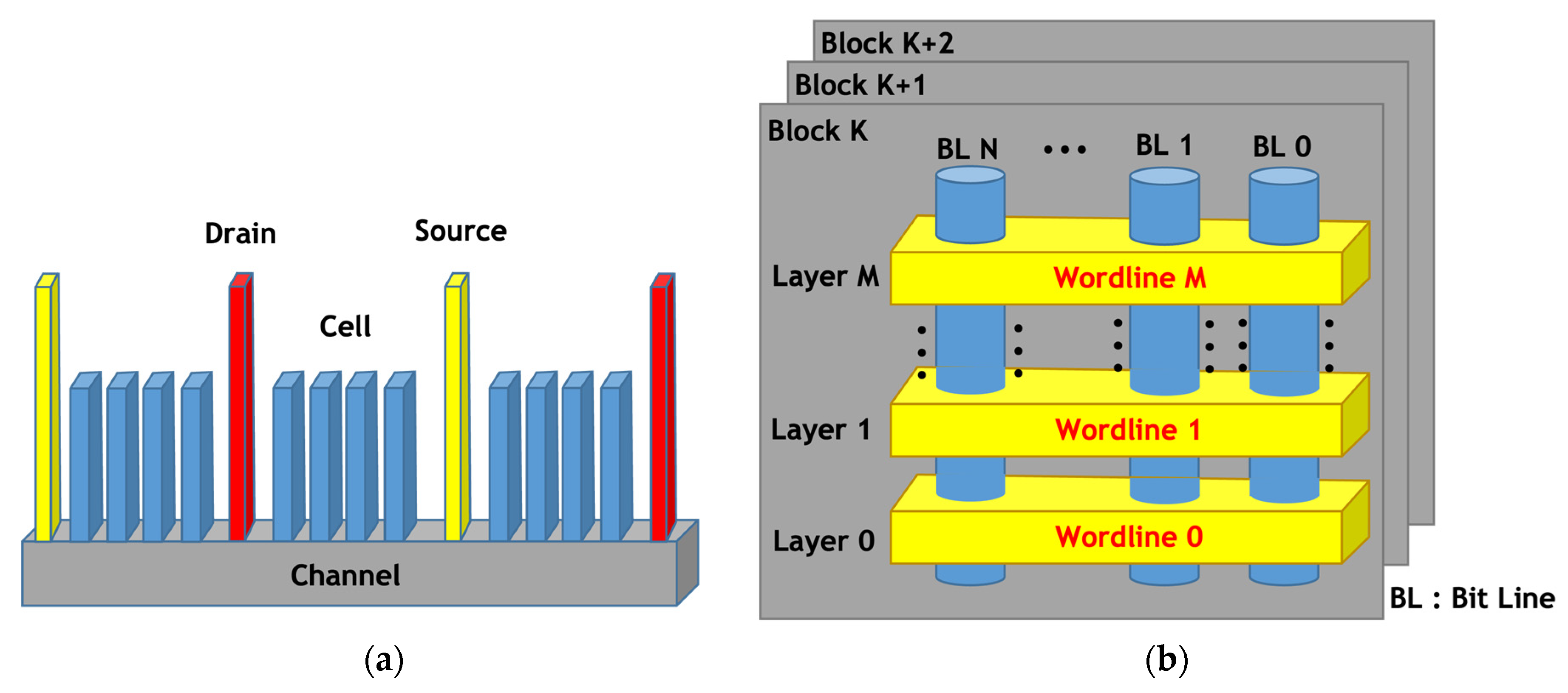
Figure 1 shows the structure of 2D- and 3D-NAND flash memory [
2].
Figure 1a shows the structure of 2D-NAND flash memory. It consists of a cell for storing data, a channel providing pathway for electrons transportation, and a drain and source providing a path for electron movement on the application of voltage to the cell. Conversely, 3D-NAND flash memory is made into a three-dimensional structure by stacking 2D-NAND flash memory, and one layer is called a layer. The blue cylindrical model in
Figure 1b was created by vertically rotating the existing 2D-NAND flash memory. Storage capacity per unit space has increased significantly compared with 2D-NAND flash memory because of the three-dimensional design and process. Wordline, as shown in
Figure 1b, is a passage through which the voltage applied to each cell passes. It can be seen that wordline and bit line are orthogonal to each other.
One layer consists of upper, middle, and lower pages. Like 2D-NAND, 3D-NAND flash memory has several planes and dies, and one die consists of several blocks, and one block consists of several pages.
2.3. Reliability Issues Due to the Process-Variation of 3D-NAND Flash
3D-NAND flash memory is manufactured by stacking planar (2D) NAND cells. However, because of the nature of the stacking process, the frequency of errors may vary depending on each layer or cell location when the layers are stacked in this manner [
1]. This problem can be influenced by factors such as structure distortion during processing, channel hole bending, and a change in the diameter of the channel hole from the upper layer to the lower layer. These process issues are representative factors that can affect flash memory reliability [
2,
3].
As a method to cope with 3D-NAND process variation, an error prediction method using machine learning [
16] and LI-RAID [
5] have been proposed. The error prediction method [
16] predicts an error level through machine learning based on the raw bit error measured for each block and allocates a block group to be used according to the predicted level. LI-RAID [
5] is the most similar to our proposed differentiated protection policy and it composes pages with different error rates into one stripe to keep the error rates of all stripes uniformly. The difference between LI-RAID and the proposed method is to adjust the protection strength by adjusting the number of parities. We believe that our proposed policy is a more flexible configuration.
2.4. Error Rate Pattern according to P/E Cycles of 3D-NAND Flash
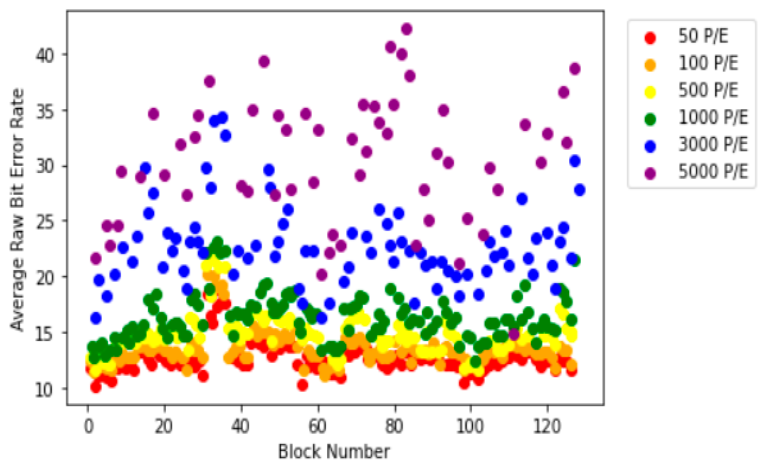
Yuqian Pan et al., designed a NAND flash test platform with Xilinx Zynq-7020 and tested blocks on different chips of 3D-TLC flash memory [
16].
Figure 2 depicts the distribution of error rates revealed in the papers by Yuqian Pan et al. [
16]. In this figure, we show the average error rate as a function of block number, ranging from 50 to 5000 P/E cycles. The figure shows that the difference in average BER by block does not appear significantly below 1000 P/E cycles but as the number of P/E increases, the difference enlarges.
2.5. Number of Errors per Page and Layer
Zambelli et al., showed that the number of errors in 3D TLC NAND flash differs for each layer and page [
1].
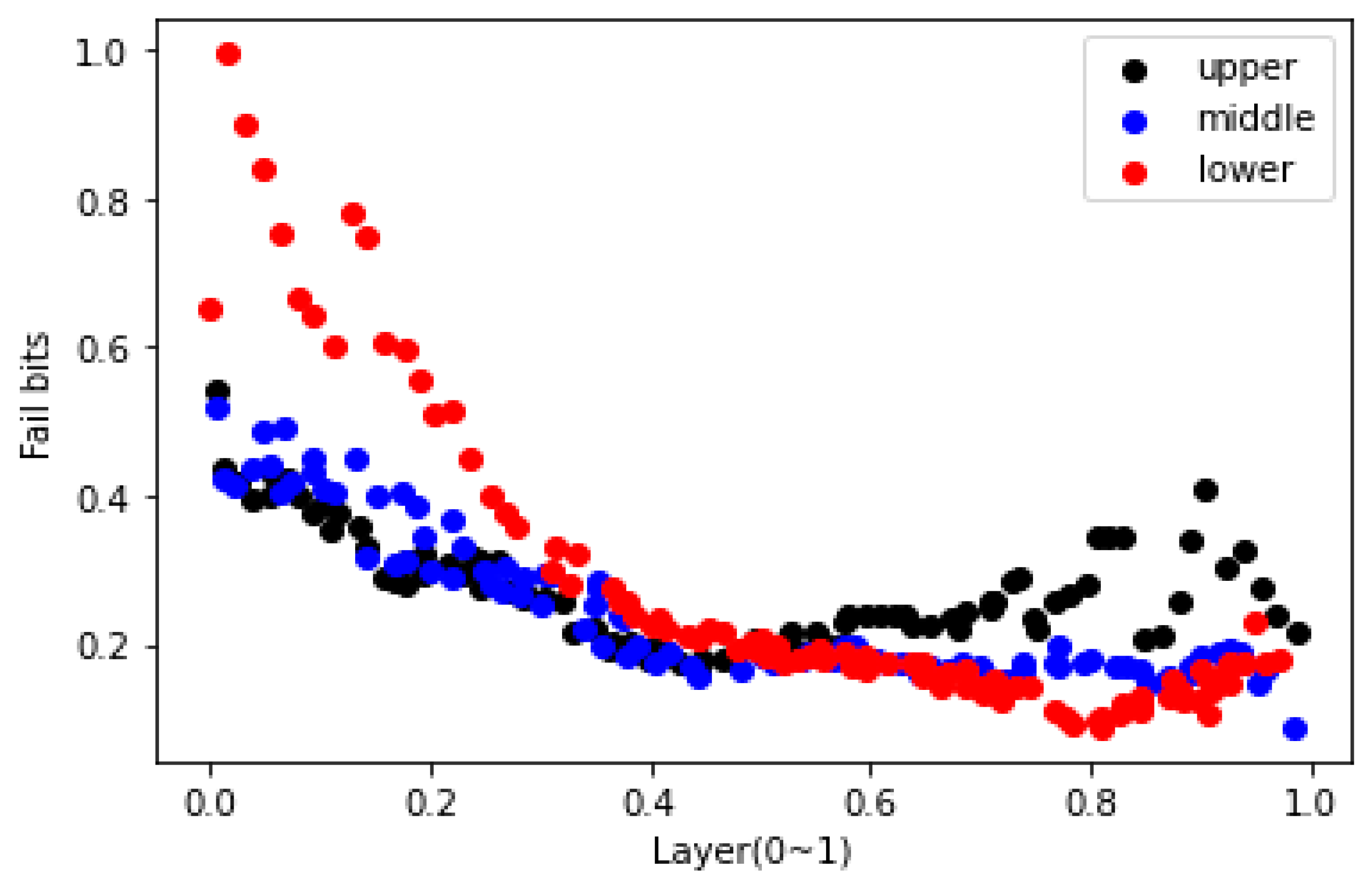
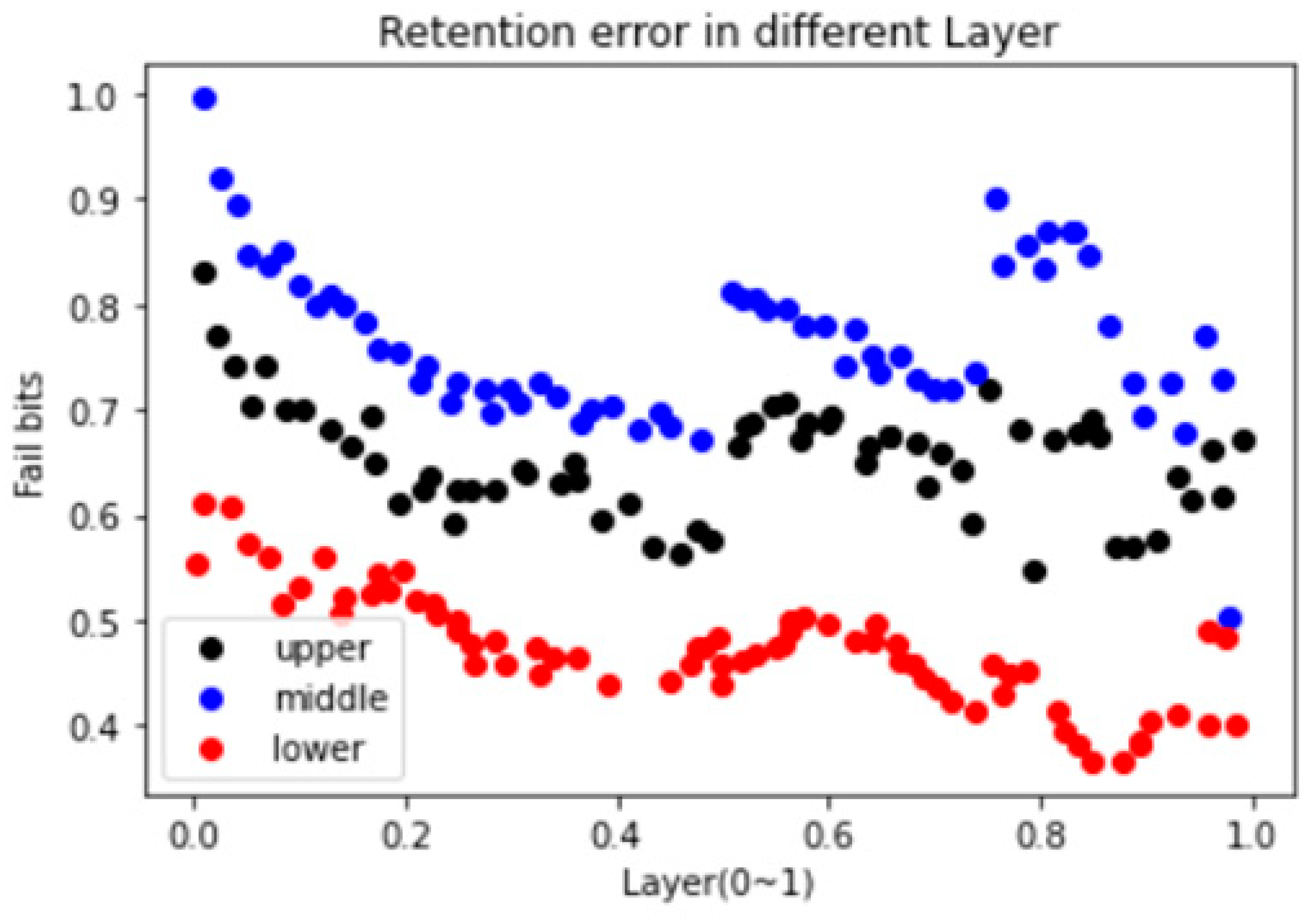
Figure 3 is a distribution chart of the number of errors reported by Zambelli et al. [
1]. Endurance testing is a procedure that determines the number of incorrect bits for each page and layer after repeatedly writing and erasing a memory block in a random pattern.
Figure 3 depicts an error bit distribution measured at the end of the endurance test reported by [
1]. The
x-axis layers in
Figure 3 range from 0 to 1. The closer the layer is to 0, the lower the layer, and the closer the layer is to 1, the higher the layer. Furthermore, the Fail bits represent the number of times an error occurred, and it is expressed as a relative value ranging from 0 to 1. The black, blue, and red dots represent the top, middle, and bottom of the page, respectively. We can see the characteristics of the errors that occur in each layer in
Figure 3. The lower page has the most errors in the lower layer, and the number of errors occurs regardless of the page type. Conversely, in the middle layer, you can see that the number of error occurrences for each page is comparable. In addition, in the upper layer, it can be seen that the upper page has the most number of errors and the lower page has the least number of errors.
2.6. K-means Cluster Analysis Based on Error Rate
As shown in
Figure 3, 3D-NAND flash has a characteristic that the number of errors is different for each page and layer. The reliability of 3D-NAND flash memory can be improved by applying a clustering algorithm to classify according to this characteristic and using a data protection policy suitable for the characteristics of each cluster.
There are various types of clustering algorithms, such as k-means, mean shift, Gaussian mixture model, and DBSCAN. Among them, the graph in
Figure 3 was used as input data and classified using the k-means algorithm, which is easy and concise, and generally used frequently (see
Figure 4) [
17]. The
x-axis in
Figure 4 represents layers from 0 to 1. A value closer to 0 means the lower layer and a value closer to 1 means the upper layer. The
y-axis indicates the number of error occurrences as Fail bits, and it is expressed as a relative value from 0 to 1 as in
Figure 3.
In the k-means algorithm, the number of clusters is determined according to an arbitrary
k value determined by the user, and similar clusters are classified only by the distance between the input data. The k-means algorithm seeks a set of data that minimize the variance of each cluster. Looking at how the k-means algorithm classifies clusters, the user determines the center point of the clusters as much as the
k (the number of clusters) value based on the first input data (here, the data in
Figure 3). The data closest to each centroid are then classified into the same cluster using the Euclidean distance formula. The previously determined
k center points are repositioned in the center of the newly classified cluster. Until the center point cannot be moved any further, the data closest to each center point are newly classified into the same cluster, and the process of moving the center point is repeated.
We adopt a heuristic way of increasing k by 1 to find an appropriate k. In this way, we obtain k values with clear error rate cluster identification. Result of classification, when the k value was 6 (the number of clusters was 6), areas according to the error rate were clearly identified.
2.7. Write Amplification Factor (WAF)
Another reason to use a data protection policy that is differentiated according to the characteristics of each cluster is related to the performance of the SSD. If our goal is simply to lower the error rate, we can apply the maximum data protection strength to all clusters. However, doing so will increase WAF because of indiscriminate parity data writing and adversely affect performance.
WAF stands for write amplification factor. WAF is the ratio of writes generated by an actual device (i.e., flash memories) to user write. In addition to simply writing data, the operation of finding and writing a new location in the flash memory for reading, updating, and rewriting data takes place. Consequently, even if the user attempts to write
n bytes,
n +
a bytes are written inside the flash memory. WAF has a significant impact on flash memory storage I/O (Input and Output) performance; that is, as WAF increases, I/O performance decreases [
12]. Parity data writes are another factor that increases WAF, which increases the number of P/E cycles, resulting in faster wear [
12]. Rather than adding parity data to all clusters to reduce error rates, performance and reliability should provide differentiated data protection strength by selectively adding parity data based on the number of errors in each cluster.
2.8. Retention Error
A retention error is a data error caused by the loss of retained electric charge. When data is stored on a flash memory page and read after a certain period, the data value changes because of the loss of electric charge retained in the data. In terms of retention error, the error rate rises as retention time increases. The retention error tends to increase rapidly until about 11 days after data is written, after which the error increase rate tends to decrease [
5]. Furthermore, because of the nature of the error, retention error occurs more frequently for cold data, where data update is difficult once it is stored on a page than for hot data, where data update occurs frequently. Consequently, by storing hot data in an area prone to retention errors, the error rate can be effectively reduced.
Figure 5 is the retention error distribution of 3D TLC NAND flash, which is reported by Zambelli et al. [
1]. From the figure, it is obvious that the number of errors on the middle page is higher, whereas the number of errors on the lower page is relatively low. It can be seen that the number of errors on the upper page is less than on the middle page but greater than on the lower page. The overall distribution clearly indicates that the number of error occurrences is relatively high in the lower, middle, and 0.82–0.85 layers. Additionally, the number of errors in the upper layer is relatively low. Therefore, it can be seen that the areas vulnerable to retention errors are the middle page and the upper page of the lower, middle, and upper-middle layers.
There have been several studies [
5,
6,
18,
19,
20] to reduce retention error, and the most similar technique to the proposed method is WARM [
6]. WARM proposes a write-hotness aware retention management policy. It classifies hot and cold write data through a window-based algorithm to mitigate refresh overhead, which significantly increases the internal write amount of flash memory. WARM increases the lifespan of flash memory by selectively performing refresh only for write-cold. It exploits the property that write-hot data requires a shorter retention time guarantee. Similar to WARM, our proposed hot/cold-aware data placement policy utilizes data hotness. The difference is that we exploit the error rate differentiation according to the physical location of 3D NAND to place hot- and cold-data at high and low retention error rates, respectively.
3. The Proposed Scheme
This section explains how to apply a differentiated protection policy to an SSD using 3D-NAND flash memory and a structure for arranging hot/cold data by identifying areas vulnerable to retention errors. Prior to the description, parity data is redundant data for error correction that is stored in the same stripe as user data when a page in a stripe is stored. When an error occurs in a specific piece of data in a stripe and the corresponding data cannot be read, the data in which the error occurred can be restored using the parity stored in the same stripe. Consequently, adding parity data can both lower the error rate and increase reliability. In
Section 4, we investigated how much the error rate can be reduced by incorporating parity with analytic formulas.
3.1. Differentiated Data Protection Policy Structure
First,
Figure 6 briefly shows a general SSD internal structure to illustrate the proposed structure. It is assumed that five flash memory chips are connected by a channel to the SSD controller, and the block is configured as four pages. As shown in
Figure 1 and
Figure 3, one layer has a lower, middle, and upper page, and the error rate varies by page and layer.
Figure 4 depicts six clusters classified by the k-means algorithm based on the characteristics of these 3D-NAND flash memories to apply differentiated data protection strength based on error rates. If numbering the clusters in order from top left to right, depending on the error rates, the stripe of the first cluster sets the parity to
n, the stripe of 2, 3, and 6 clusters sets the parity to
n − 1, and the stripe of 4 and 5 clusters sets the parity to
n − 2 to apply the differentiated data protection strength [
14].
Assuming
n (by analyzing the error incidence analysis introduced in
Section 4, the number of parity per stripe can be adjusted to achieve the desired reliability level) is 2, one stripe spans five flash memory chips. If flash memory blocks corresponding to the first cluster of the error occurrence are represented as shown in
Figure 6c, it applies to the lower page of the lower layer. Similarly, the flash memory chip stripe corresponding to clusters 2, 3, and 6 can be expressed as
Figure 6a,c, and it applies to all pages of the upper layer and to the upper and middle pages of the lower layer. If the flash memory chip stripe corresponding to the 4 and 5 clusters has a low number of error occurrences, it can be represented as
Figure 6b and applies to all pages of the middle layer. The first cluster that has the most number of error occurrences sets the data protection strength highest by setting the number of parity data per stripe (
n parity). For 2, 3, and 6 clusters, where the number of error occurrences is middle, the number of parity data per stripe is set to
n − 1, and set the data protection strength of middle. Finally, for the 4 and 5 clusters that have the lowest number of error occurrences, the number of parity data per stripe is set to
n − 2. So, specifies differentiated data protection strength for each cluster. The management methods of striping and partial stripe parity for partial data follow the recent efficient log structure writing schemes [
12,
14]. Differentiated protection policy should be similar to the efficient log write methods. Details will be discussed in
Section 5.3.
3.2. Hot/Cold-Aware Data Placement Structure
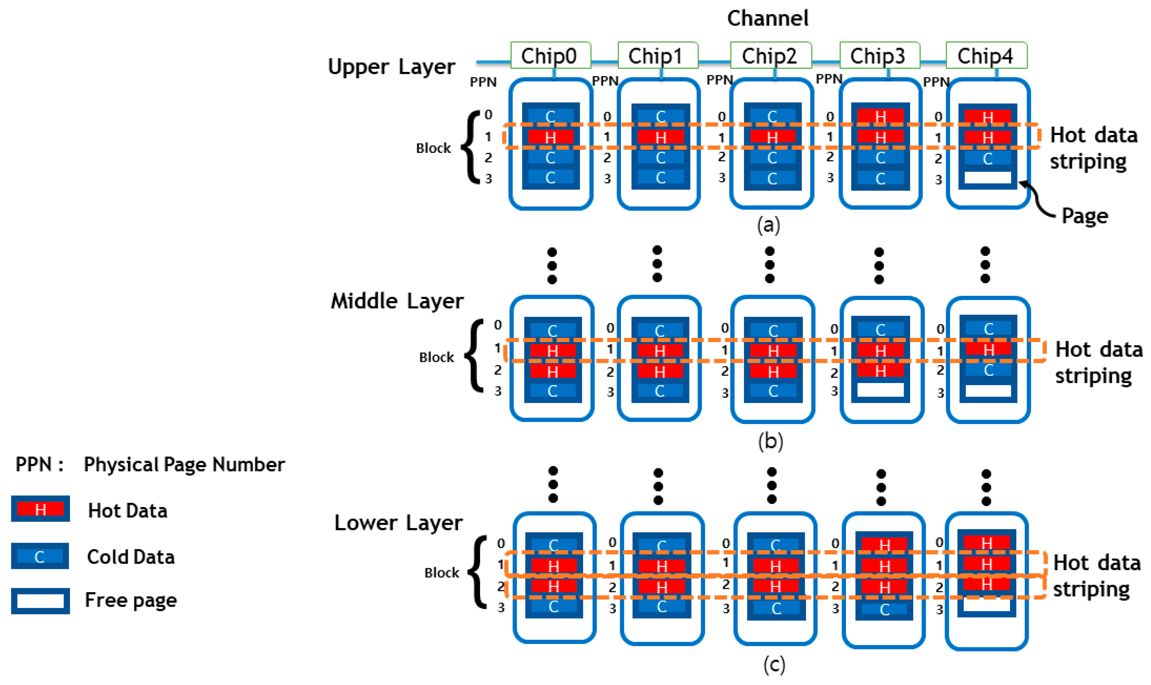
As can be seen in
Figure 5, retention error is also seen that the number of errors occurs differently by page and layer. It can be seen that the middle and upper pages have a relatively high number of errors, whereas the lower page has a relatively low number of errors. When looking at the number of errors by layer, it is clear that the lower layer has the highest number of errors. The middle and upper pages of the lower layer are vulnerable to the retention error, as are the middle and upper pages of the middle and upper layers, as well as the lower layer.
Retention error means an error that occurs when data is stored on the flash memory page and then read data after a certain period. This mostly happened with cold data, which is data that has been stored but has no access to it. Conversely, hot data is a relatively frequent update to the data in a short period after the data is stored on the page, and the probability of occurrence of retention error is low. If we arrange cold and hot data, we place hot data in a relatively vulnerable area to retention error.
In
Figure 7, we present a data placement structure we proposed. We assume that cold and hot data exist at a ratio of 50% for the sake of simple notation. We also assume that the SSD is made up of five flash memory chips and that one block is made up of four pages, as shown in
Figure 7. Let us start with the lower layer, which is the most vulnerable to the retention error. We use hot data striping on the middle page, which has the highest number of retention errors. Furthermore, if new hot data arrives, it can be placed on an empty upper page. Then, let us consider the middle layer, where the retention error rate is lower than the lower layer but more than the upper layer. Similarly, we can see that hot data is organized on the middle page. However, since the retention error rate of the middle layer is lower than that of the lower layer, it can be seen that the number of hot data is relatively smaller than the lower layer. Finally, let us look at the upper layer that the number of errors is relatively the least shown. Hot data, like other layers, is placed first in the middle pages where the most errors occur. As the lower page of the upper layer is less vulnerable to the retention error, many cold data have been placed. Furthermore, because the number of errors is lower than in the middle layer, the number of hot data is lower. Additional overhead with the proposed policy will be discussed in
Section 5.3.
3.3. Relationship between Two Policies
The differentiated data protection policy and hot/cold-aware data placement technique presented in this paper can be independent and complementary data protection policies. The differentiated data protection policy can be applied flexibly and dynamically in response to changes in the error rate. For example, it can be selectively applied to the early and late stages of SSD by adjusting the data protection strength based on the change in the number of P/E cycles of the flash memory or depending on the bathtub model that appears in most systems. The hot/cold-aware data placement can consistently deal with retention errors throughout the SSD’s lifetime.
4. Analysis of Reliability of SSDs
In this section, we explain analytic formulas used to analyze the ECC that protects data using only the existing ECC and RAID-like protection model that provides differentiated data protection strength (we also refer to this as Differentiated Protection in this work) in terms of error rates.
The raw bit error rate (
RBER) of flash memory increases exponentially with the P/E cycle period as follows. In this equation,
x represents the P/E cycle of the block, and
A and
B are constant values depending on the type and process of the flash memory [
14].
ECC codes can correct errors up to
k bits per
n-specific code words. If ECC can correct
k bits errors. The correctable page error rate
(CPER) that ECC can correct from 0 bit error to
k bits error rate, can be calculated with a binary distribution as follows [
12,
14].
Furthermore, there is a
k + 1 or more bits error rate that ECC cannot correct, the uncorrectable page error rate
(UPER) is as follow [
12,
14].
ECC has a limitation that ECC cannot correct errors when the number of error bits exceeds k, and errors that cannot be corrected by ECC are corrected through RAID parity. In addition, to correct the error through RAID parity, the error must first be detected through ECC.
ECC can correct errors up to
k bits and detect errors up to 2
k bits. This is generally valid because coding theory supports this claim [
12]. Additionally, assume that SSDs using RAID architecture can correct errors with parity only when a page has bit errors less than or equal to 2
k. Therefore, although it cannot be corrected, the detectable page error rate that can be detected by ECC is defined as follows [
14].
There are two cases in which bit errors in the stripe can be corrected. The first case is when all pages containing a stripe have less than or equal to
k bits errors. A case in which an error of
k bits or less occurs in all pages containing a stripe can be corrected by ECC, and the probability of occurrence, in this case, is defined as follows [
21].
The second case is when
N − 1 pages of the stripe have
k bits or fewer errors that occur, and one page has more than
k bits and no more than 2
k bits errors occur. The probability of occurrence, in this case, is as follows [
21].
If there is no parity per stripe (only ECC is provided), the error bit will be corrected only by the ECC of the stripe page, so the
UPER in the ECC model is as follows.
N stands for stripe size, if there is one parity per stripe: (1) When only bit errors that can be corrected by ECC occur in the striped page, and (2) ECC detectable errors occur on one page of the stripe and ECC correctable errors occur on the remaining pages. Since errors can be corrected in these two cases, the
UPER is as follows [
14].
In the case where two parities per stripe are maintained, if two-page errors that can be detected by ECC occur at the same time, both pages can be modified at the same time, so the
UPER is as follows [
14].
6. Conclusions
In this paper, we present two error handling techniques considering the characteristics of 3D-NAND flash memory. As the frequency of error occurrence varies by page and layer when ECC is used collectively, the efficiency of error correction decreases. Furthermore, one of the layers is more or less vulnerable to retention error, and this characteristic significantly affects the deterioration of the flash memory’s reliability [
1].
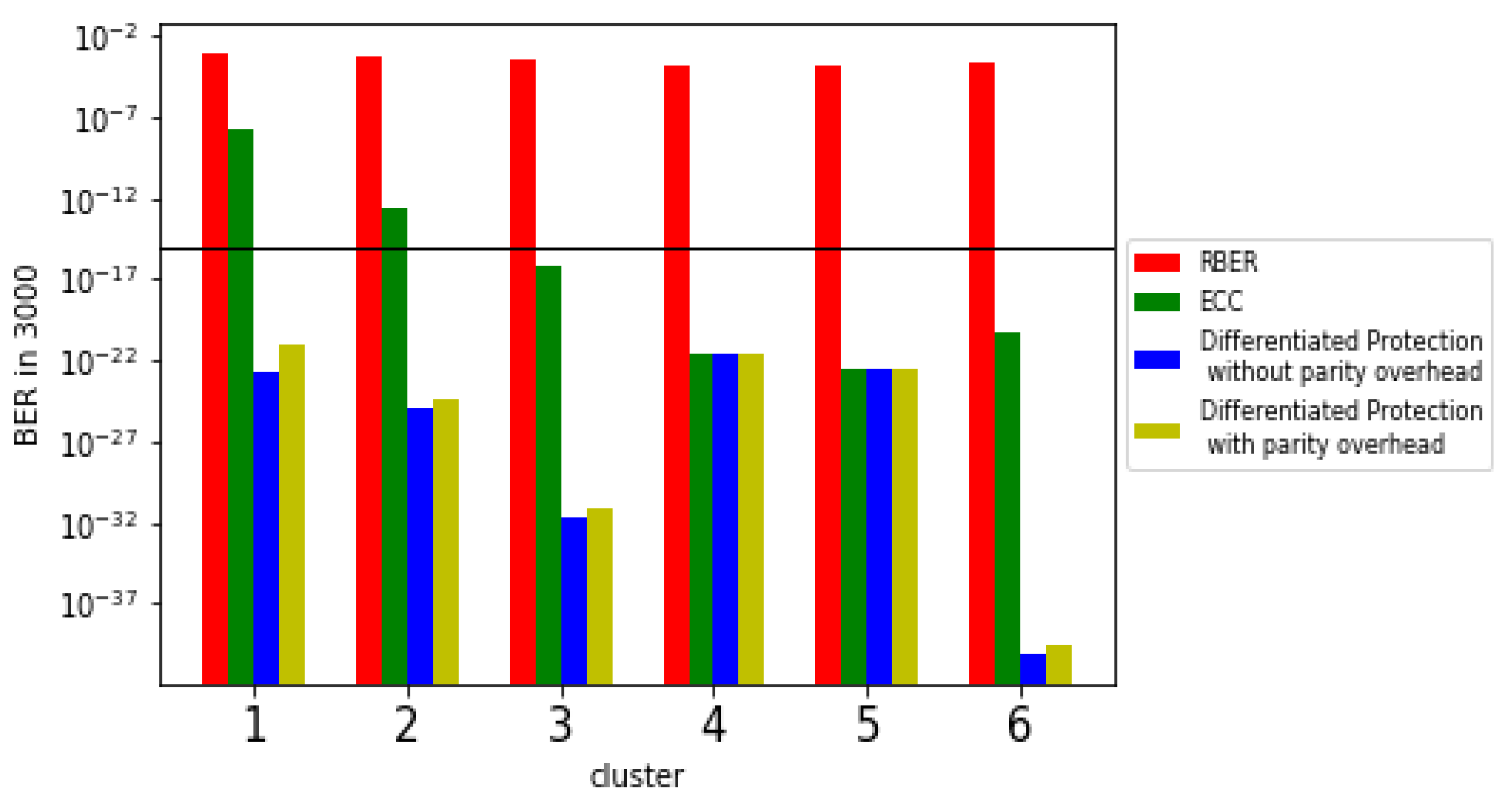
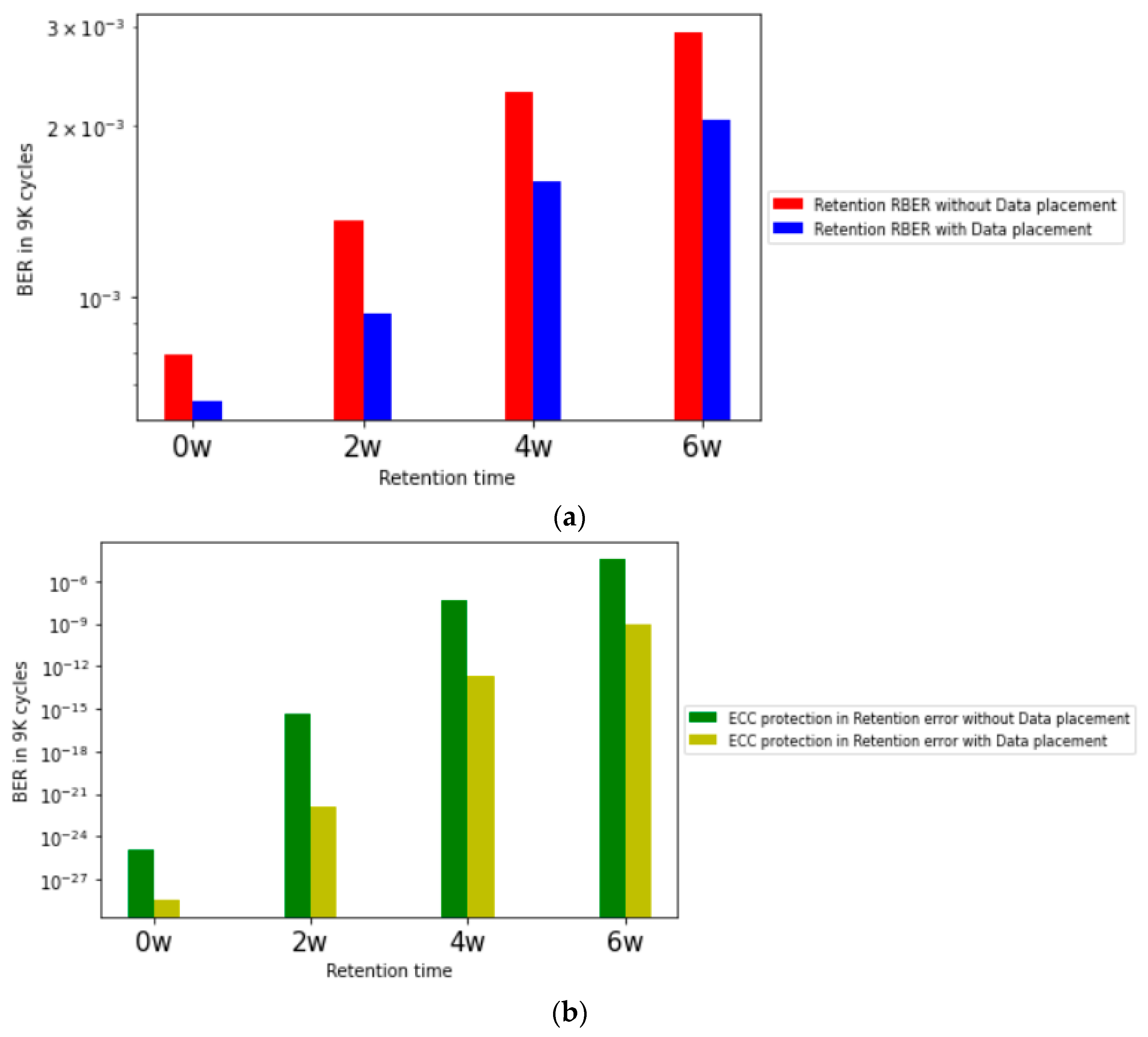
We present the number of errors after the endurance test, which shows the characteristics of different error rates for each page and layer. It shows that the ECC operation that provides the same data protection strength to the pages of the flash memory is not suitable. In addition, by classifying the data through the k-means clustering algorithm, the regions are classified according to the number of errors, and the differentiated protection strength is applied by adding parity data. The SSD model that protects data using only the existing ECC and the Differentiated Protection model we proposed are evaluated in terms of error rates. Through the distribution of the number of occurrences of retention errors, the hot data are placed to areas that are relatively more vulnerable to retention errors. Based on 9K P/E cycles, it is shown that the BER caused by retention error is lowered and the data placement structure and Differentiated Protection model presented in the paper improve the reliability of 3D-NAND flash memory through quantitative evaluation.


