Article

A Deep Learning Approach for Efficient Electromagnetic Analysis of On-Chip Inductor with Dummy Metal Fillings

Engineering Research Center of Smart Microsensors and Microsystems, Ministry of Education, School of Electronics and Information, Hangzhou Dianzi University, Hangzhou 310018, China
*
Authors to whom correspondence should be addressed.
Electronics 2022, 11(24), 4214; https://doi.org/10.3390/electronics11244214
Submission received: 18 November 2022 / Revised: 6 December 2022 / Accepted: 15 December 2022 / Published: 16 December 2022

Abstract

:
A deep learning approach for the efficient electromagnetic analysis of an on-chip inductor with dummy metal fillings (DMFs) is proposed. By comparing different activation functions and loss functions, a deep neural network for DMF modeling is built using a smooth maximum unit activation function and log-cosh loss function. The parasitic capacitive effect of DMFs is quickly and accurately extracted though this model, and the effective permittivity can be obtained subsequently. An on-chip inductor containing DMFs with different filling densities is analyzed using this proposed method and compared with the electromagnetic simulation of entire structures. The results validate the accuracy and efficiency of this proposed method.

1. Introduction

Chemical mechanical polishing (CMP), a key step in modern integrated circuit (IC) processes, allows for the homogenization and flattening of metal and dielectric thicknesses [1,2]. In order to meet the CMP process requirements and achieve a uniform metal density, it is necessary to fill the areas of lower metal density with additional dummy metal. However, DMFs introduce additional parasitic capacitances and resistances [3,4], which increase the coupling with the on-chip structures and degrade the chip performance. The accurate modeling of the DMF effect using an electromagnetic (EM) solver can lead to the huge consumption of computational resources such as CPU time and memory requirements, which is unacceptable in IC designs.
Typically, the effect of DMF is simulated through an equivalent circuit of on-chip passive components or by using numerical methods to equate the DMF to an effective dielectric constant to avoid the significant time and resources spent in calculating the DMF directly using EM simulation. In [5], the parasitic parameters of DMFs were extracted based on the measured data to construct an equivalent circuit, and then predict the inductor characteristics containing DMFs. In [6], the parasitic parameters of DMFs were extracted based on the PEEC modeling method [7], and then an equivalent circuit model was constructed for the analysis of the inductors containing DMFs. However, the method proposed in [5,6] was only applicable to a fixed metal filling density. In [8], on-chip inductors containing DMFs were modeled by using a single π-circuit model, but the method used a simple formula to extract the parasitic capacitance of DMFs, and the model accuracy was low. In [9], the on-chip inductor containing DMFs was modeled by using a double-π circuit model, but this method requires a separate calculation of the S-parameters of the inductor containing and not containing DMFs, which is a very tedious modeling process. A simple capacitance extraction formula was proposed in [10,11], but the formula is only applicable for the signal line modeling. An empirical formula was proposed in [12], which is applicable to floating metal filling between flat plates, and the key parameters of this empirical formula were obtained by least-squares fitting by the measured data, so this formula does not have good generality.
In this work, a method for constructing an equivalent model containing DMFs using deep neural networks (DNNs) is proposed. By comparing the performance of different activation and loss functions, the smooth maximum unit (SMU) activation function and log-cosh loss function are used in the proposed method, because this combination performs better than the traditional Rectified Linear Unit (Relu) [13] activation function and mean squared error (MSE) [14] loss function. After constructing a DNN capacitance extraction model containing DMF (DNN-DMF model), the capacitance increments introduced by different densities of DMFs can be quickly and accurately evaluated, and then DMFs can be equated to the effective permittivity of the surrounding medium, which can get rid of the time-consuming dummy simulation while ensuring accuracy. This equivalent modeling method is only related to the filling density of DMFs and can be applied to IC simulation, e.g., inductors containing DMFs. Finally, the effectiveness of the proposed modeling approach is verified using full-wave calculations of inductors containing DMFs and is compared with the single-π circuit modeling approach in [8].

2. Neural Network Equivalent Model

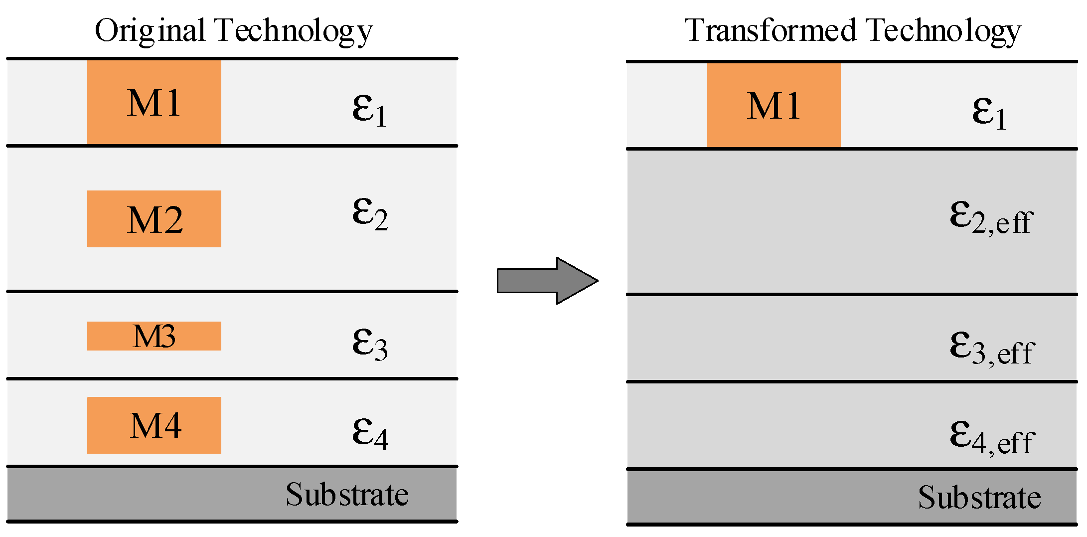
2.1. Equivalent Relative Permittivity

As shown in Figure 1, if the metal dummy fill is located at layers M2, M3 and M4, the permittivity of the corresponding layered dielectric medium can be replaced by an effective permittivity, and the influence of the metal fill is contained in the effective permittivity.
The effective relative permittivity can be obtained by calculating the capacitance values before and after the virtual metal filling [15]:
ε r , e f f = C M F C N o M F · ε r , I L D
where ε r , e f f is the effective relative permittivity, ε r , I L D is the relative permittivity of the surrounding inter-layer dielectric (ILD), C M F is the unit cell capacitance with metal fill and C N o M F is the unit cell capacitance without metal fill.

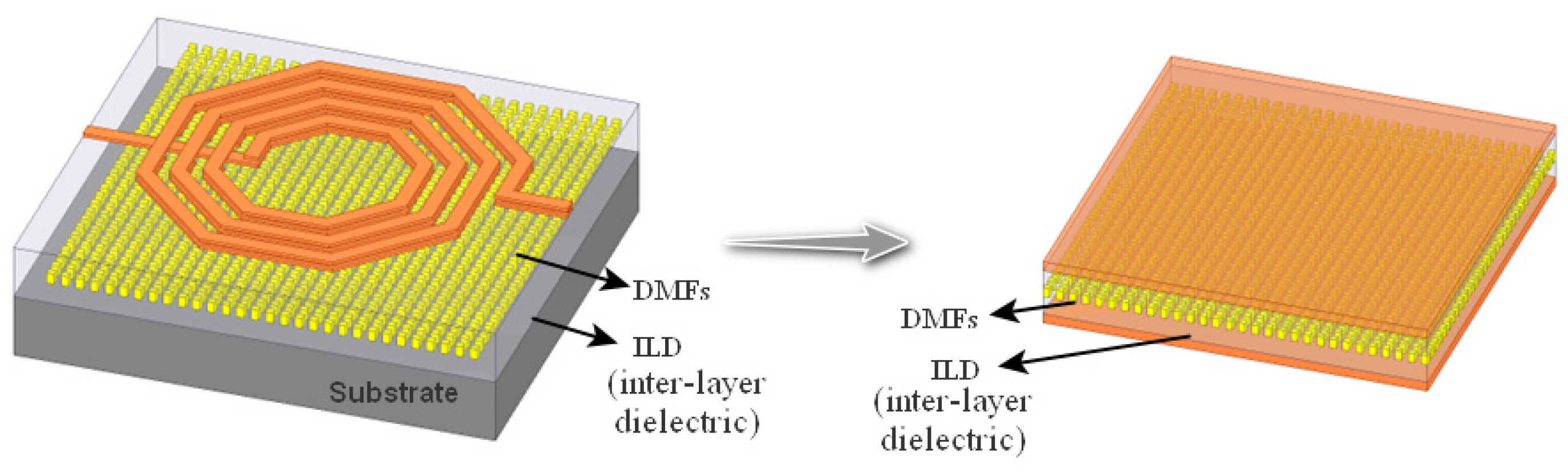
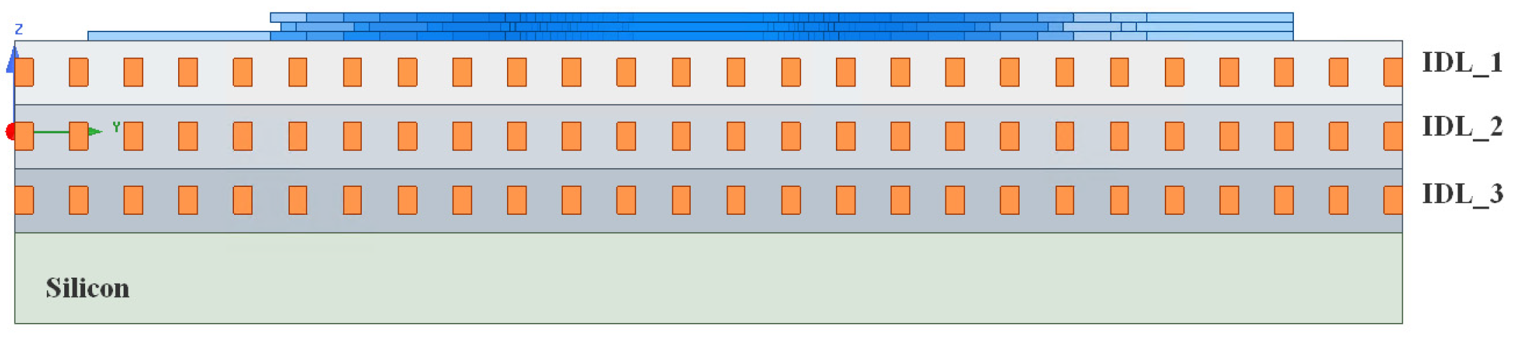
2.2. Equivalent Flat Capacitance Model with DMFs

If the capacitance with and without (multilayer-) DMF is calculated according to the actual structure of IC, and then obtains the overall equivalent permittivity, it is not universal because if the structure changes, the capacitance needs to be recalculated. The effective permittivity is calculated layer by layer. For each DMF layer, a flat capacitor is added to cover the DMF region. Since the additional parasitic capacitance is introduced by the DMFs, the incremental capacitance can be calculated equivalently using a flat capacitor containing the same DMF process. After evaluating the effective permittivity, the simulation of the IC devices can be simulated without containing the geometry of DMFs, and thus the simulation is very highly efficient.
A schematic diagram for constructing an equivalent flat capacitor model based on the original inductor containing DMFs is shown in Figure 2. The equivalent flat capacitor covers the DMFs with the original surrounding interlayer dielectric. The length and width of the top and bottom metal plates equal the total length and width of the DMF array.

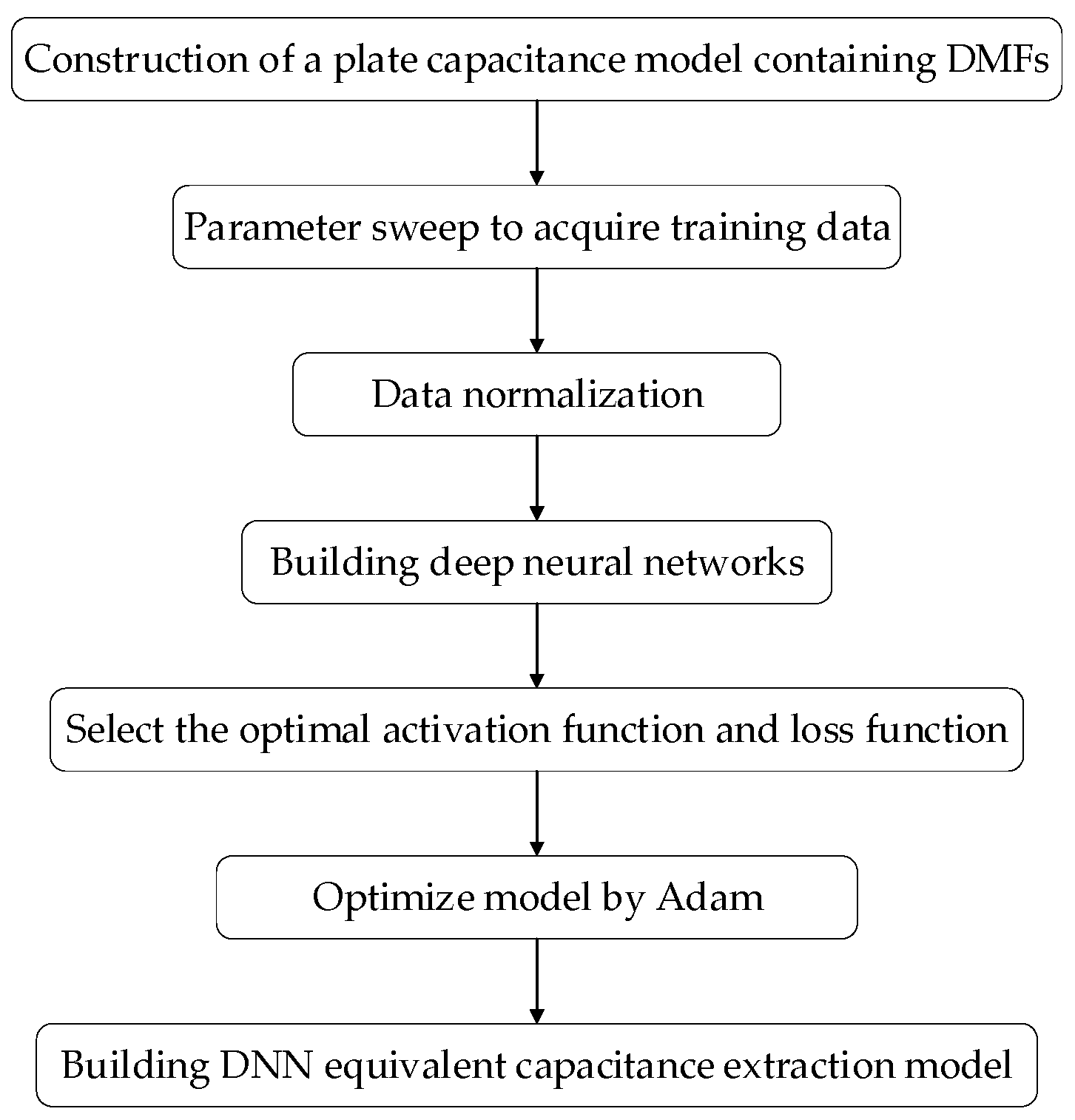
2.3. Construction of DNN Capacitance Extraction Model Containing DMF (DNN-DMF Model)

Figure 3 shows the flow chart of the DNN-DMF training model. A flat capacitor model is built for each DMF layer. After building the parameterized DMF structures, some typical DMFs with the sampling filling density are chosen, and the capacitance with the DMFs is calculated. The calculated capacitance with the corresponding filling density of DMFs and the original permittivity are the training and testing data of the DNN. Once the DNN-DFM model is built, the capacitance for the different filling densities of the DMFs and the surrounding permittivity is quickly obtained. Compared with the capacitance without DMF, the effective permittivity is evaluated using (1).

2.3.1. Deep Neural Network Model

In the DNN, the neurons are used as components of the neural network and the mathematical expression is:
Y = φ ( i n a i X i + b )
where X i denotes the i-th element of the input matrix; a i represents the weight factor of the i-th element; b is the offset.
The deep neural network model is made up of multiple layers of neurons connected in pairs between adjacent layers. The mathematical expression of a complete neural network can be expressed as:
Y = φ ( A n φ ( A 2 ( φ ( A 1 X + b 1 ) ) + b 2 ) + b n )
where φ represents the activation function, which can introduce nonlinear factors into neurons and be used to fit various nonlinear models, X denotes the geometric parameters of the DMF layer (inputs to the neural network) and Y denotes the corresponding capacitance value of the equivalent flat capacitor model containing DMF (outputs to the neural network). In the field of deep learning, the Relu function is the mostly used activation function due to its simplicity and good convergence. However, the output of Relu is not zero centered, and it is easy to have neuron death failure during the training process. As the recently proposed activation functions, the ELU [16], Mish [17] and SMU [18] activation functions have some advantages in modeling. The definitions of these functions are shown in (4)–(7).
E L U ( x ) = { e x 1 ,   x < 0 x , x 0
M i s h ( x ) = x · tan h ( l n ( 1 + e x ) )
S M U ( x , α x ; μ ) = ( 1 + α ) x + ( 1 α ) x · e r f ( μ ( 1 α ) x ) 2
In the expression of SMU, α and μ can be hyperparameters or trainable parameters, and in this paper we set α and μ as 0.01 and 2.5, respectively. e r f is the Gaussian error function defined as follows:
e r f ( x ) = 2 π 0 x e t 2 d t
In this work, the Relu, ELU, Mish and SMU activation functions are used for the training of DNN-DMF equivalent flat capacitance models, and the performance of these activation functions will be compared later.

2.3.2. Loss Function and Optimization Algorithm

The role of the loss function is to calculate the difference between the forward calculation result of each iteration of the neural network and the true value to guide the next training step in the right direction, and it will also be used to check the accuracy of the model. As a widely used loss function, the MSE function is applied to many general regression problems [19]. However, because MSE squares the error, it will aggravate the error of outlier samples and lead to the slow or even non-convergence of the model. The loss function of the log-cosh type is another loss function applied in regression problems, which is smoother than MSE. This function combines the advantages of MSE and mean absolute error (MAE), reduces the sensitivity to outliers, and enhances the robustness of the neural network model to outliers. The log-cosh loss function is defined as follows:
L ( y , y p ) = i = 1 n log ( cosh ( y i p y i ) )
where y is the actual value; y p is the predicted value. In training the DNN-DMFs model, y represents the real capacitance in the dataset and y p represents the capacitance obtained from the DNN-DMFs model.
Next, the loss function is minimized using the Adam [20] optimization algorithm, and the training error of the loss function is reduced by continuously adjusting the weight factors and offsets in the neural network with the loss function as the objective function during the optimization process to improve the accuracy of the network model.

2.3.3. Training DNN-DMF Model

A parametric flat capacitance model containing DMFs is established as shown in Figure 4, where WD denotes the width of each filler metal, SD denotes the spacing between the adjacent filler metals, TD denotes the thickness of the filler metals and Tox denotes the distance between the filler metals and the upper and lower flat plates. The aforementioned four geometric parameters of DMF will be swept to provide the training data of the DNN-DMF model, and the scanning range of geometric parameters is shown in Table 1. After training the DNN-DMF model, the corresponding capacitance increments introduced by DMFs can be quickly obtained by inputting any geometric parameter in the range of Table 1, and then the DMFs’ effect can be equated to the increase in surrounding permittivity. As these four geometrical parameters are swept in Table 1, the testing final error can be guaranteed if the DMFs do not exceed the parameter range. Although the DNN can predict the EM parameters even outside the range of the geometrical training data, the testing final error is not guaranteed. In other words, this model is able to apply the DMF distribution if the WD, SD, TD and Tox are from 1 μm to 5 μm. The model may be invalid if the DMF distribution exceeds the training range or the IC technology changes, e.g., the dielectric layer changes or the number of dummy layers increases. Under these circumstances, the model requires to be re-established.
The actual convergence performance of the DNN-DMF model using different combinations of the activation and loss functions is compared in Table 2. In this table, the final test loss is set as the criterion of convergence. As can be seen from Table 2, for different activation functions, the log-cosh loss function always achieves a smaller test loss compared with the MSE. That is because the log-cosh loss is smoother than the MSE, and it will decrease the sensitivity to the outliers and consequently enhance the robustness of the neural network to the outliers. Moreover, among the listed activation functions, only the SMU activation function has two adjustable hyperparameters α and μ. These two hyperparameters provide flexibility to fit the DNN-DMF problem more easily (α = 0.01 and μ = 2.5 in this problem). As a result, even using the same log-cosh loss function, the SMU activation function performs better than the other three functions, and can satisfy the error threshold of 1 × 10 6 .

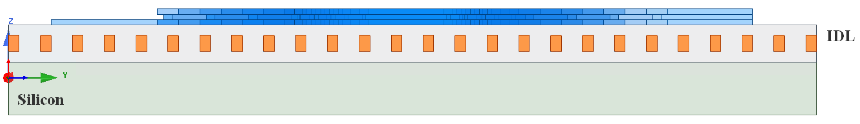
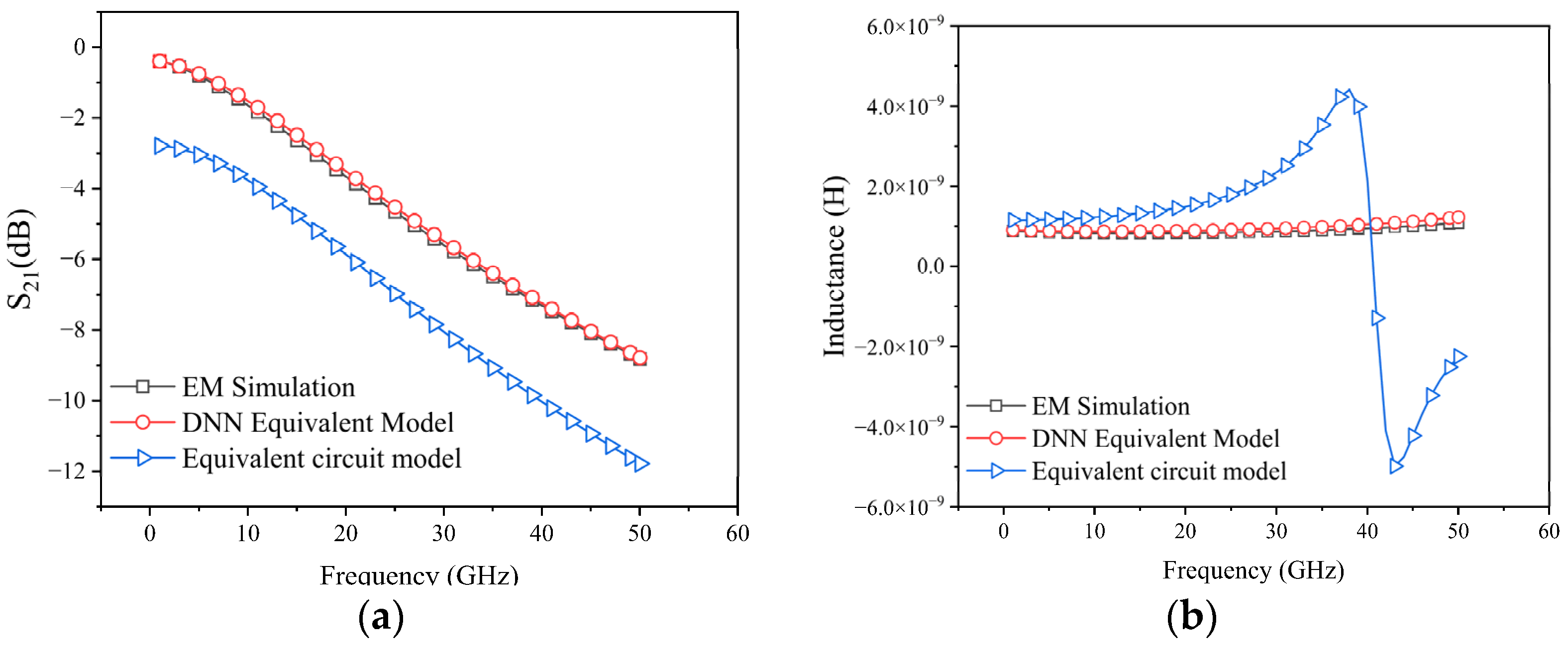
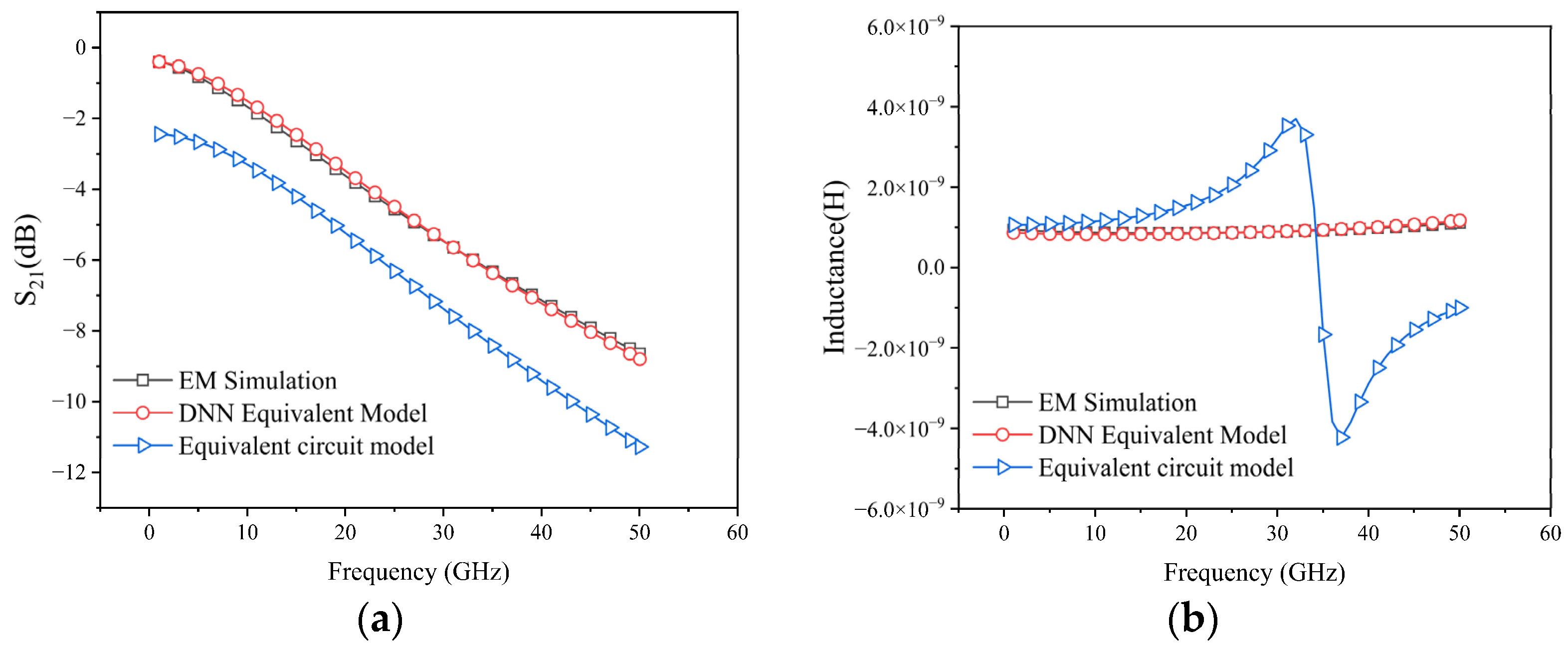
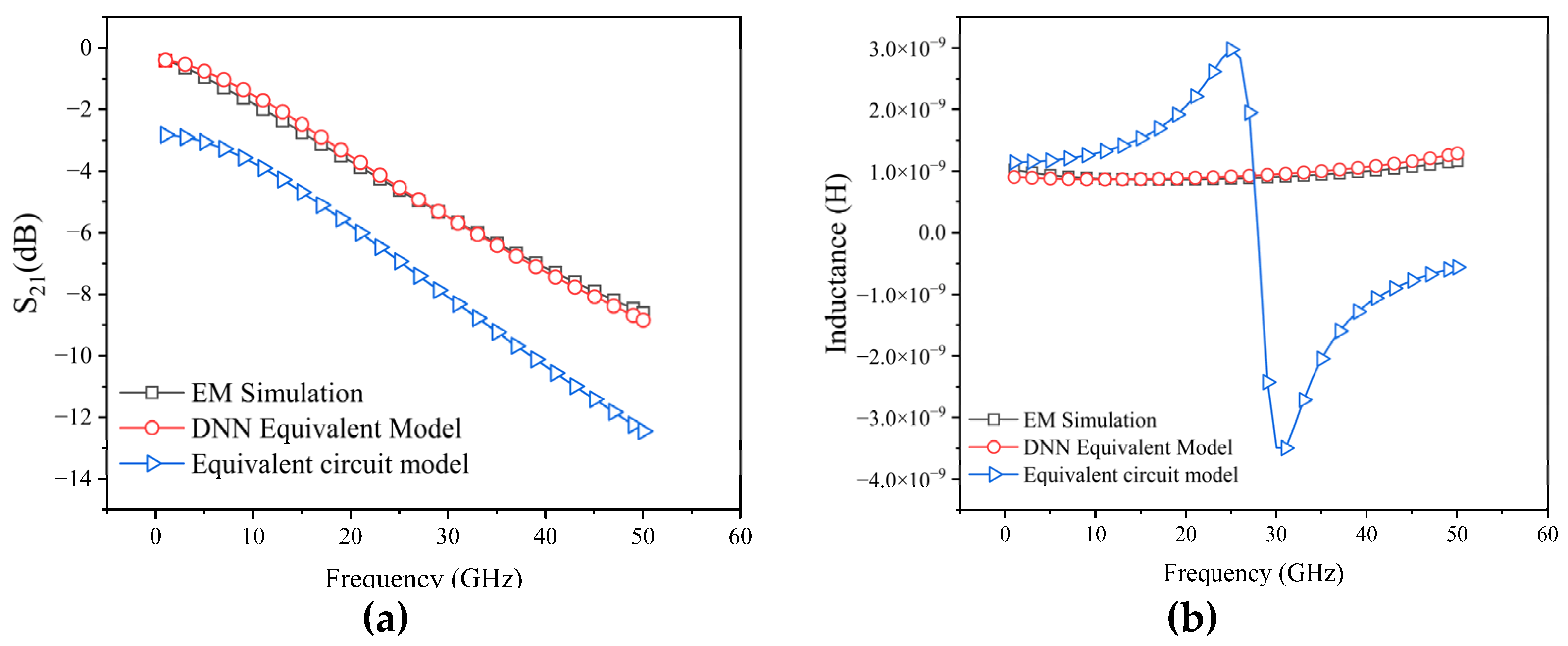
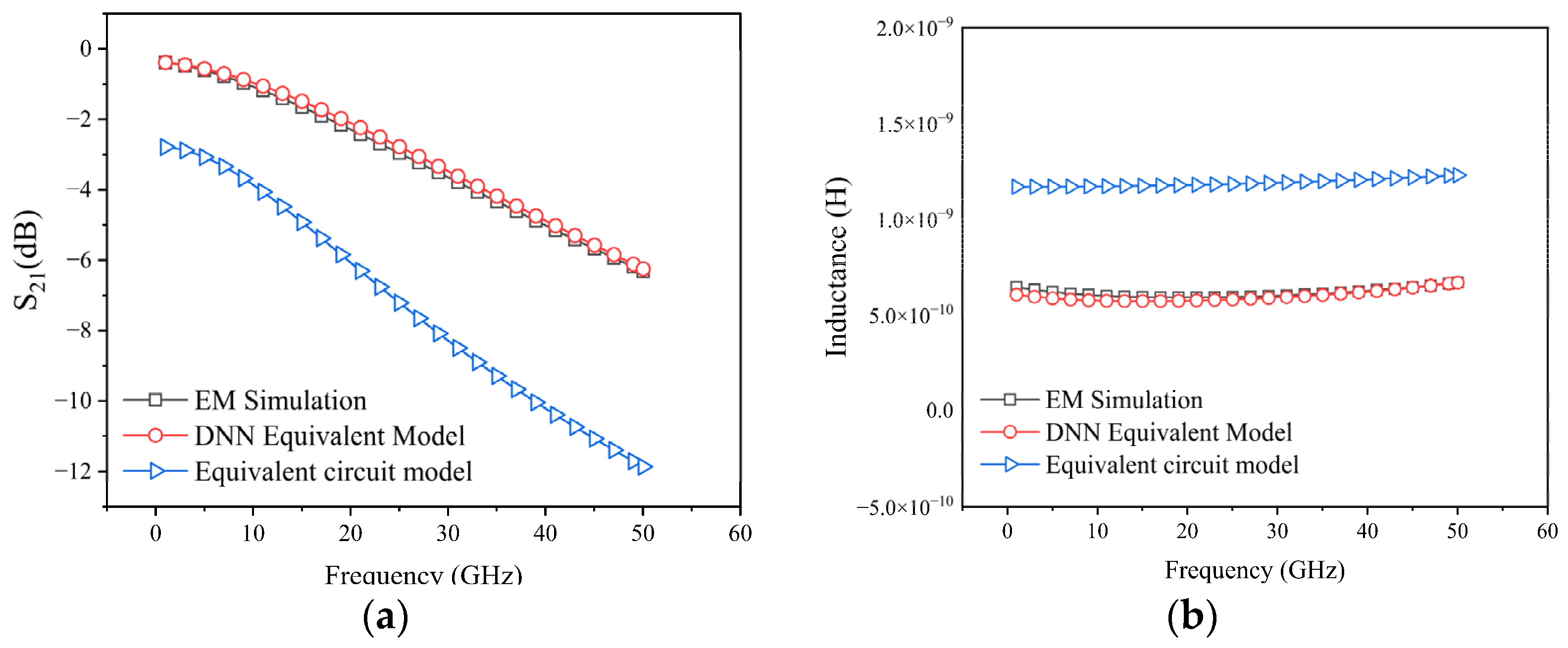
3. Validation of DNN Equivalent Model

The capacitance increments introduced by DMFs with different filling densities can be quickly obtained using the DNN-DMF model so that the DFM can be equated to an increase in the permittivity of the surrounding dielectric layer to avoid EM calculations for DMFs. In Figure 5, on-chip inductors containing different DMF densities are calculated using the equivalent permittivity method based on the DNN-DMF model, and a single π-circuit model is constructed as shown in Figure 6, and then the effectiveness of both methods is verified using EM simulations. In this example, the geometric parameters are as the following: ind equals 20 μm, w equals 2 μm and d equals 2 μm. The spacing between the DMFs layer and the on-chip inductor metal layer, i.e., Tox, is equal to 1 μm. The DMF layer thickness TD is equal to 1.5 μm. When the dummy width and spacing (i.e., WD and SD) change and make the metal filling densities 20%, 50% and 80%, the ratio of capacitance values ( C M F / C N o M F ) for the three metal filling densities is shown in Table 3, and the parameters of the lumped device for the single-π circuit model are shown in Table 4, where for the capacitance of the oxide layer containing DMF we use Equation (4) in [9]. In calculation, the effect of the crosstalk capacitance Cs is negligible [21].
Figure 7 gives the side view of the inductor filling one DMF layer. The capacitance increment introduced by the DMF can be easily obtained using the DNN-DMF model, and once the capacitance increment has been determined the DMF can be equated to the effective permittivity using (1). The S-parameters (S21) and inductance values of the on-chip inductors with 20%, 50% and 80% DMF densities calculated by the effective permittivity method based on the DNN-DMF model and the single π circuit model equivalent method were verified using direct EM simulations of the complete structure containing DMFs, as shown in Figure 8, Figure 9 and Figure 10, respectively. It can be seen that the results obtained using the equivalent permittivity method based on the DNN-DMF model are very close to those obtained using direct EM simulations, but the single-π equivalent circuit model has a large error. This may because the capacitance Cox introduced by the DMF is calculated using a simple numerical formula, and the mutual coupling between the DMF layers is not considered in the equivalent circuit model.
Moreover, the inductor containing three layers of DMFs with a 20% fill density, as shown in Figure 11, was analyzed, and the accuracy of the DNN-DMF model was verified, with a large error in the same single π equivalent circuit model method. The S-parameters (S21) and inductance values for two methods are shown in Figure 12.
In Table 5, the computation cost listed in the DNN-DMF model does not include the deep learning process. To train the DNN-DMF model, it takes about 43 min and occupies the memory of 1.4 MB. It is observed that the training time is less than the EM simulation except in case 3 in the table. Moreover, the trained DNN-DMF model can be applied to a category of DMF problems, e.g., cases 1 to 3 are not required to be re-trained. After building the DNN-DMF model, it takes about 3 s to obtain the effective dielectric constant, and the total computation cost including the EM simulation using the effective dielectric constant is compared with the full structure EM simulation in Table 5. To further improve the accuracy of the DNN-DMF model, the simplest and most effective way is to increase the number of training sets by increasing the scan parameters, which can further improve the convergence of the model, but this will also increase the training time of the DNN-DMF model. In addition, the development of better performance activation and loss functions is also an effective way of improving the accuracy of the DNN model.

4. Conclusions

In this work, the deep learning network is applied to the EM analysis of on-chip inductors containing DMFs. A DNN-DMF model considering the dummy effect of the effective dielectric constant is proposed to approach the EM simulation, and get rid of the time-consuming dummy simulation. Different activation and loss functions were compared to obtain better accuracy of the DNN-DMF model, and it was found that the combination of the SMU activation function and log-cosh loss function performs best in the accuracy of capacitance evaluation. Using the DNN-DMF model and the further derived effective dielectric constant, the S-parameters and inductance of the on-chip inductor containing DMF can be efficiently calculated. Some examples of inductors containing different DMF filling densities and numbers of layers were given to validate the accuracy and efficiency of the proposed method.

Author Contributions

Conceptualization, X.L., Y.T. and P.Z.; Data curation, X.L.; Funding acquisition, P.Z.; Investigation, X.L. and Y.T.; Methodology, X.L.; Project administration, X.L.; Supervision, P.Z., S.C., K.X. and G.W.; Writing—original draft, X.L.; Writing review and editing, X.L., Y.T., P.Z., S.C., K.X. and G.W. All authors have read and agreed to the published version of the manuscript.

Funding

This work was supported in part by the National Natural Science Foundation of China under Grant 62141409, Grant 61971171 and 61971174 in part by the Zhejiang Provincial Key Research & Development Project under Grant 2021C01041.

Conflicts of Interest

The authors declare no conflict of interest.

References

  1. Fury, M.A. Emerging Developments in CMP for Semiconductor Planarization. Solid State Technol. 1995, 38, 81–86. [Google Scholar]
  2. Stine, B.E.; Boning, D.S.; Chung, J.E.; Camilletti, L.; Kruppa, F.; Equi, E.R.; Loh, W.; Prasad, S.; Muthukrishnan, M.; Towery, D.; et al. The Physical and Electrical Effects of Metal-Fill Patterning Practices for Oxide Chemical-Mechanical Polishing Processes. IEEE Trans. Electron Devices 1998, 45, 665–679. [Google Scholar] [CrossRef] [Green Version]
  3. Lee, K.H.; Park, J.K.; Yoon, Y.N.; Jung, D.H.; Shin, J.P.; Park, Y.K.; Kong, J.T. Analyzing the Effects of Floating Dummy-Fills: From Feature Scale Analysis to Full-Chip RC Extraction. In Proceedings of the Technical Digest—International Electron Devices Meeting, Washington, DC, USA, 2–5 December 2001. [Google Scholar]
  4. Kim, Y.; Petranovic, D.; Sylvester, D. Simple and Accurate Models for Capacitance Considering Floating Metal Fill Insertion. IEEE Trans. Very Large Scale Integr. (VLSI) Syst. 2009, 17, 1166–1170. [Google Scholar] [CrossRef]
  5. Hsu, H.M.; Hsieh, M.M. On-Chip Inductor above Dummy Metal Patterns. Solid-State Electron. 2008, 52, 998–1001. [Google Scholar] [CrossRef]
  6. Shilimkar, V.S.; Gaskill, S.G.; Weisshaar, A. Scalable Modeling of On-Chip Spiral Inductors Including Metal Fill Parasitics. In Proceedings of the IEEE MTT-S International Microwave Symposium Digest, San Francisco, CA, USA, 30 May 1984–1 June 1984. [Google Scholar]
  7. Ruehli, A.E. Equivalent Circuit Models for Three-Dimensional Multiconductor Systems. IEEE Trans. Microwave Theory Techn. 1974, 22, 216–221. [Google Scholar] [CrossRef]
  8. Wang, Y.; Chen, B.; Liu, S.; Lou, L.; Tang, K.; Zhang, Y.; Zheng, Y. Analysis and Modelling on CMOS Spiral Inductor with Impact of Metal Dummy Fills. In Proceedings of the 14th International Symposium on Integrated Circuits, ISIC 2014, Singapore, 10–12 December 2014. [Google Scholar]
  9. Chen, D.; Wu, Y.; Liu, H.; Yin, W.-Y.; Kang, K. A Scalable Model of On-Chip Inductor Including Tunable Dummy Metal Density Factor. IEEE Trans. Compon. Packag. Manufact. Technol. 2019, 9, 296–305. [Google Scholar] [CrossRef]
  10. Kim, Y.; Petranovic, D.; Sylvester, D. Simple and Accurate Models for Capacitance Increment Due to Metal Fill Insertion. In Proceedings of the Asia and South Pacific Design Automation Conference, ASP-DAC, Yokohama, Japan, 23–26 January 2007. [Google Scholar]
  11. Kurokawa, A.; Kanamoto, T.; Kasebe, A.; Inoue, Y.; Masuda, H. Efficient Capacitance Extraction Method for Interconnects with Dummy Fills. In Proceedings of the Custom Integrated Circuits Conference, Orlando, FL, USA, 6 October 2004. [Google Scholar]
  12. Gaskill, S.G.; Shilimkar, V.S.; Weisshaar, A. Accurate Closed-Form Capacitance Extraction Formulas for Metal Fill in RFICs. In Proceedings of the Digest of Papers—IEEE Radio Frequency Integrated Circuits Symposium, Boston, MA, USA, 7–9 June 2009. [Google Scholar]
  13. Brownlee, J. A Gentle Introduction to the Rectified Linear Unit (ReLU) for Deep Learning Neural Networks. Available online: https://machinelearningmastery.com/rectified-linear-activation-function-for-deep-learning-neural-networks/ (accessed on 15 October 2022).
  14. Guan, Z.; Zhao, P.; Wang, X.; Wang, G. Modeling Radio-Frequency Devices Based on Deep Learning Technique. Electronics 2021, 10, 1710. [Google Scholar] [CrossRef]
  15. Lee, W.S.; Lee, K.H.; Park, J.K.; Kim, T.K.; Park, Y.K.; Kong, J.T. Investigation of the Capacitance Deviation Due to Metal-Fills and the Effective Interconnect Geometry Modeling. In Proceedings of the Proceedings—International Symposium on Quality Electronic Design, ISQED, San Jose, CA, USA, 24–26 March 2003. [Google Scholar]
  16. Clevert, D.A.; Unterthiner, T.; Hochreiter, S. Fast and Accurate Deep Network Learning by Exponential Linear Units (ELUs). In Proceedings of the 4th International Conference on Learning Representations, ICLR 2016—Conference Track Proceedings, San Juan, Puerto Rico, 2–4 May 2016. [Google Scholar]
  17. Misra, D. Mish: A Self Regularized Non-Monotonic Activation Function. In Proceedings of the 31st British Machine Vision Conference, Manchester, UK, 7–10 September 2020. [Google Scholar] [CrossRef]
  18. Biswas, K.; Kumar, S.; Banerjee, S.; Pandey, A.K. Smooth Maximum Unit: Smooth Activation Function for Deep Networks Using Smoothing Maximum Technique. In Proceedings of the 2022 IEEE/CVF Conference on Computer Vision and Pattern Recognition (CVPR), New Orleans, LA, USA, 18–24 June 2022. [Google Scholar]
  19. Girod, B. Psychovisual Aspects of Image Processing: What’s Wrong With Mean Squared Error. In Proceedings of the Seventh Workshop on Multidimensional Signal Processing, Lake Placid, NY, USA, 23–25 September 1991. [Google Scholar]
  20. Kingma, D.P.; Ba, J.L. Adam: A Method for Stochastic Optimization. In Proceedings of the 3rd International Conference on Learning Representations, ICLR 2015—Conference Track Proceedings, San Diego, CA, USA, 7–9 May 2015. [Google Scholar]
  21. Yue, C.P.; Wong, S.S. Physical Modeling of Spiral Inductors on Silicon. IEEE Trans. Electron Devices 2000, 47, 560–568. [Google Scholar] [CrossRef]
Figure 1. Conversion of metal filling into equivalent relative permittivity.
Electronics 11 04214 g001
Figure 2. Schematic diagram of the equivalent flat capacitor model, with the original inductor containing DMFs on the left and the equivalent flat capacitance containing the same DMF process on the right.
Electronics 11 04214 g002
Figure 3. Flow chart for building DNN capacitance extraction model containing DMF.
Electronics 11 04214 g003
Figure 4. Parametric flat capacitance model with DMFs.
Electronics 11 04214 g004
Figure 5. Top view of an inductor containing DMFs.
Electronics 11 04214 g005
Figure 6. Single π circuit model.
Electronics 11 04214 g006
Figure 7. Side view of an inductor containing only one layer of DMFs.
Electronics 11 04214 g007
Figure 8. S-parameters (S21) and inductance values for a metal filling density of 20%; (a) shows S-parameters (S21) and (b) shows inductance values.
Electronics 11 04214 g008
Figure 9. S-parameters (S21) and inductance values for a metal filling density of 50%; (a) shows S-parameters (S21) and (b) shows inductance values.
Electronics 11 04214 g009
Figure 10. S-parameters (S21) and inductance values for a metal filling density of 80%; (a) shows S-parameters (S21) and (b) shows inductance values.
Electronics 11 04214 g010
Figure 11. Side view of an inductor containing three layers of DMFs.
Electronics 11 04214 g011
Figure 12. S-parameters (S21) and inductance with three layers of DMFs and a metal filling density of 20%; (a) shows S-parameters (S21) and (b) shows inductance values.
Electronics 11 04214 g012
Table 1. Sweep Parameters.
Input ParametersStarting ValueEnd ValueStep
WD (μm)151
SD (μm)151
TD (μm)151
Tox (μm)151
Table 2. Comparison of the convergence of different activation functions and loss functions when training DNN equivalent flat capacitance models containing DMFs.
Test LossMSELog-Cosh
Relu 9.04 × 10 6 2.49 × 10 6
ELU 5.09 × 10 5 1.14 × 10 5
Mish 9.98 × 10 6 3.06 × 10 6
SMU 4.84 × 10 6 8.81 × 10 7
Table 3. The ratio of capacitance before and after metal filling for different metal filling densities.
Metal Filling Densities C M F / C N o M F
20%1.26
50%1.46
80%1.53
Table 4. Parameters of lumped devices for single π-circuit model at different DMF densities.
Metal Filling DensitiesRs(Ω)Ls(pH)Rsub(Ω)Csub(pF)Cox(fF)
20%37.621.1736.572.512.9
50%32.291.0830.512.6619.35
80%38.241.1837.322.4826.57
20% (Triple DMF)37.621.1736.572.54.3
Table 5. Comparison of the efficiency of the EM simulation and the method proposed in this paper.
MethodNumber of Layers of DMFsMetal Filling DensityTimeMemory
EM Simulation120%54 min306 M
DNN-DMFs120%73 s77.5 M
EM Simulation150%78 min678 M
DNN-DMFs150%59 s77.1 M
EM Simulation180%28 min378 M
DNN-DMFs180%79 s76.9 M
EM Simulation320%118 min497 M
DNN-DMFs320%72 s77.6 M
Publisher’s Note: MDPI stays neutral with regard to jurisdictional claims in published maps and institutional affiliations.

