Article

Silicon-Germanium Heterojunction Bipolar Transistor DC and AC Analysis Operating under Cryogenic Temperature

Department of Electrical Engineering, Indian Institute of Technology Hyderabad, Kandi 502284, India
*
Author to whom correspondence should be addressed.
Electronics 2022, 11(24), 4164; https://doi.org/10.3390/electronics11244164
Submission received: 17 October 2022 / Revised: 19 November 2022 / Accepted: 7 December 2022 / Published: 13 December 2022
(This article belongs to the Section Electronic Materials)

Abstract

:
In this work, the numerical simulation of a SiGe heterojunction bipolar transistor (HBT) for DC and AC performance operating at cryogenic temperature with a hydrodynamic carrier transport model is analyzed. A new modified temperature-dependent Si1−xGex energy bandgap model was used. Using a simplified 2D TCAD design structure, the device characteristics on 55 nm SiGe HBT technology and the mobility model are calibrated with experimental data. Base current reversal due to induced impact-ionization at the collector-base junction is analyzed, where the estimated collector-emitter breakdown voltage with the base open (BVCEO) is 1.48 V at 300 K. This reveals good voltage handling ability. At cryogenic temperatures, dopant incomplete ionization in the lightly doped collector region shows a 28% decrease in ionized dopant concentration at 50 K; this affects the base-collector depletion capacitance. The emitter electron barrier tunneling leakage on collector current is studied using a non-local e-barrier tunneling model at different temperatures that shows an improvement in peak DC gain at lower temperatures. Using the small-signal ac analysis, the cut-off frequency and the maximum oscillation frequency are extracted for high-frequency application, and the base widening effect is discussed. A comparison of this work with measured data on 90 nm SiGe HBT is also discussed in brief, which shows improvements in the simulated structure.

1. Introduction

The SiGe HBTs in advanced CMOS technology (BiCMOS) continue to be a desirable option due to their compatibility with the CMOS process flow, which expands their field of application for high-frequency communication and mixed-signal circuits [1]. The SiGe HBT shows better AC performance than Si-based CMOS in terms of lithography node, device-to-device matching improvement (i.e., less variability), and the increase in doping levels in advanced technology generations [2,3]. The advanced SiGe HBTs offer DC current gain (β), unity gain cut-off frequency (fT), and maximum oscillation frequency (fmax) of 1900/320 GHz/370 GHz for 55 nm SiGe HBT at 300 K, respectively [4,5]. The state-of-the-art SiGe HBT covers the field of cryogenic electronics with high speed and high performance applications such as radio astronomy, radar communication, and other extreme environmental conditions [6]. The experimental DC and AC performance of SiGe HBT down to 4.3 K has been reported [2,7,8], and DC evaluation has reached, experimentally, down to 70 mK [9] in 90 nm SiGe HBT technologies. However, 55 nm SiGe technology was explored at 300 K, with very few literature reports being available under cryogenic temperatures [10,11]. This paper reports the results of DC and AC analysis using numerical analysis with calibrated models. A detailed discussion on the same structure for collector-emitter saturation voltage using a hydrodynamic transport model is explored in the previous work [10]. We have analyzed different aspects (partial dopant ionization, intrinsic gain and transconductance, collector current leakage, base resistance, fT and fmax) of the SiGe HBT device from 300 K to 50 K. The advantage of cryogenic temperatures is the improvement in the operating frequency from sub-THz to THz for mm-wage/RF applications. Section 2 discusses a new modified SiGe energy bandgap model and its accuracy with respect to germanium content. Section 3 of the manuscript explores the numerical device structure, simulation methodology, and calibration. The next section discusses the impact-ionization and collector-emitter breakdown voltages with an open-circuited base (BVCEO). In Section 4.1, the impact of the dopant incomplete ionization effect on the lightly doped collector region under cryogenic temperatures is studied. The collector current (IC) due to tunneling leakage of the emitter’s electron through the emitter-base junction is investigated in Section 4.2. The AC performance metric is analyzed using small-signal AC analysis in Section 4.3. The next section discusses the comparison of the performance metrics in this work with measurement data on 90 nm SiGe HBT. Finally, conclusions are drawn in Section 5.

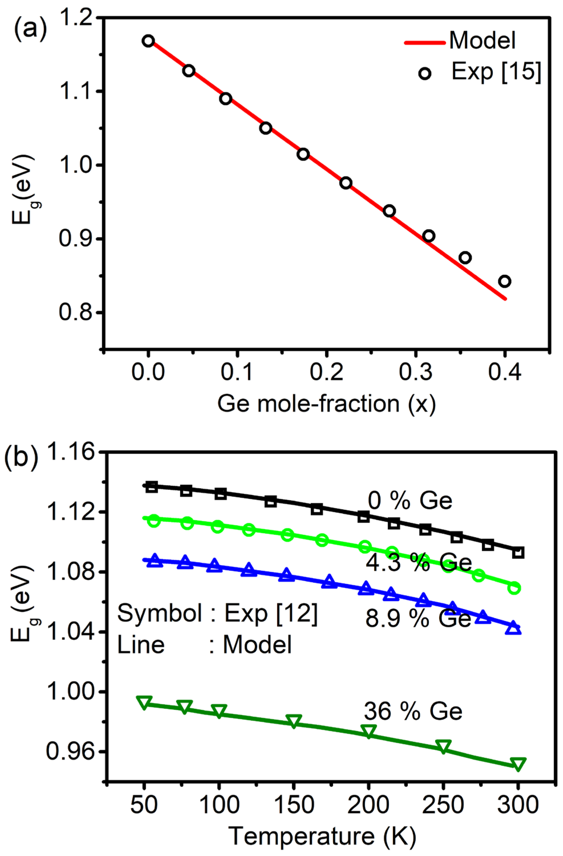
2. Energy Band Gap Model

The SiGe energy bandgap (Eg) changes with germanium (Ge) mole fraction (x) due to a lattice mismatch of 4.2% between Si and Ge. In reported work [6], an approximation has been considered for the SiGe bandgap model that, for every 10% Ge content in Si, Eg reduces by 75 meV for SiGe device design, which can tolerate up to 30% of Ge content [6]. First, an experimental study on the SiGe bandgap with Ge content and temperature dependence from optical absorption measurements is investigated by Braunstein et al. [12]. A new modified temperature and Ge mole fraction (x) dependent Si1−xGex energy band gap analytical model (1) based on Varshni [13] is used in this SiGe HBT simulation, as shown in Equation (1).
E g ( x , T ) = E g , i ( 0 ) α i T 2 β i + T 0.45 x
P i = ( 1 x ) P S i + x P G e
where Pi represent Eg,i(0), αi and βi; PSi and PGe are Si and Ge parameters, respectively, as shown in Table 1.
The mole fraction dependent term induced the energy bandgap to lower for each x consistently between 300 K–50 K, as shown in Figure 1b. In Figure 1b, a lowering of the energy band gap with increasing temperature is shown. This can also be observed in Figure 1a, which resembles that with increasing mole fraction of Ge the bandgap reduces. Both the plots in Figure 1a,b are used to validate the calibrated model for varying mole fraction and temperature parameters with reference to the energy gap. The model (1) accuracy with the experimental data [12,15] is 97% up to a Ge mole fraction of 36%, which is useful for SiGe HBT devices.

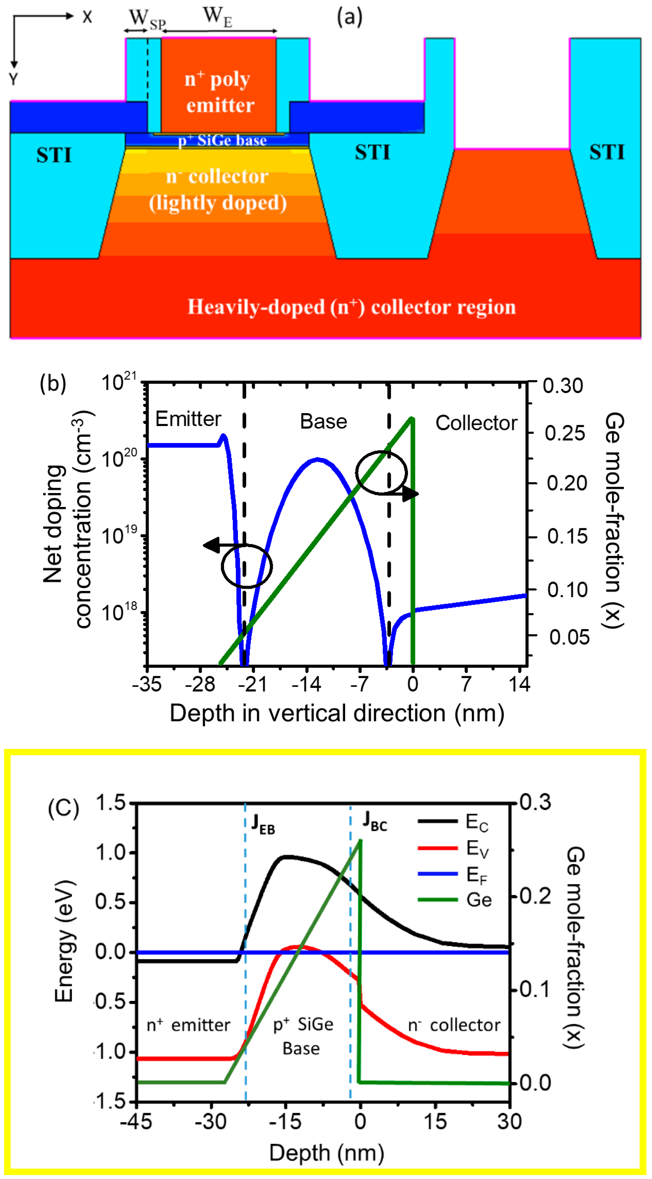
3. Numerical Device Structure and Simulation Methodology

Figure 2a shows the 2D schematic diagram of SiGe HBT with the doping profile of the intrinsic region. Numerical device dimensions and calibrated model parameters are shown in Table 2. The intrinsic collector region is lightly doped (i.e., NC = 3.0 × 1017 cm−3) in the vertical current flow direction (y-direction) to reduce the collector-base (CB) junction capacitance, whereas the intrinsic emitter region is heavily doped with peak emitter doping (NEP = 1.5 × 1020 cm−3) and has a doping gradient of 0.8 nm/dec towards the base region. In order to enhance the intrinsic drift field for electrons in the p + SiGe base, linearly graded Ge with a mole fraction (x) of 0 to 0.26 is used, as shown in Figure 2b. The epitaxial Si1−xGex layer is pseudomorphic and stable in nature using this Ge profile [16]. Figure 2c shows the equilibrium energy band diagram of n-p-n SiGe HBT with Ge profile. The blue dashed line shows the metallurgical junctions at the emitter-base and base-collector junctions, marked as JEB and JBC, respectively. The linearly graded Ge profile resulted in a bandgap (Eg) variation in the heavily doped p + −SiGe base from 1.05 eV (near the BE junction) to 0.94 eV (near the CB junction). The hydrodynamic (HD) carrier transport model is used for HBT simulations to account for the non-local nature of carrier transport under high electric fields [14]. The Slotboom model is used for a bandgap narrowing effect [14]. The temperature dependence carrier mobility models, considering carrier scattering and doping dependence in Philips unified mobility (PhU-Mob) and high-field saturation models are used [17,18,19,20,21]. The incomplete-ionization model is used in low-temperature simulations to account for active dopant concentration in the lightly doped collector region [22,23]. Recombination-generation models, such as doping and temperature-dependent SRH (Shockley–Read–Hall) and the Auger recombination model, are invoked [14]. The non-local electron barrier (e-barrier) tunneling model is used, which considers electron tunneling leakage from the BE junction barrier. In this work, the linear interpolation method for the mole fraction-dependent model parameters is used. A wide range of temperature-dependent calibrated models for Si have been considered in this work [14]. For mole fraction dependent models of materials, such as SiGe, we use linear interpolation between two parent materials, where we have calibrated the Philips unified mobility (Phu-Mob) model (θ and Nref) for p + −Si0.94Ge0.06 with a doping density of 1.0 × 1015 cm−3, and the experimental data [24] is shown in Figure 3a.
Forward Gummel characteristics, shown in Figure 3b, are reproduced with experimental data [25] at 300 K with an emitter area of 0.42 × 5.56 µm2 on 55 nm SiGe HBT. The advanced SiGe HBT in 55 nm BiCMOS uses a reduced emitter area size of 0.1 × 4.9 µm2 for the high-performance target that has been considered in our simulation. The TCAD has the facility to provide frequency dependent small-signal AC analysis with temperature-dependent physical models. The fT, fmax and junction capacitance reproduced with experimental data [4,26] are shown in Figure 3c,d on the same technology of 55 nm SiGe HBT.

BVCEO and Impact-Ionization on Base Current

The avalanche effect in the CB junction and secondary hole current due to impact-ionization results in the negative base current (−IB; base current reversal) shown in Figure 4a,b, respectively. For capturing the impact-ionization and avalanche multiplication phenomenon in the CB junction, the avalanche (Okuto) model is used [14]. In the forward active region (FAR), increasing VCB results in impact-ionization (generation of electron-hole pairs) inside the CB junction depletion region, contributing to −IB, which escapes through base contact. It is shown in Figure 4a, at VBE = 0.7 V, as VCE increases (VCB increases), −IB increases and gets subtracted from the terminal base current, resulting in a lowering of +IB. With a further increase in VCE, IB = 0 at the “notch” position (VCE = 1.48 V), where −IB = +IB; IB = 0. This VCE value for IB = 0 indicates the collector-emitter breakdown voltage with an open circuited base (BVCEO) of 1.48 V. For BVCEO, the avalanche multiplication factor (M−1 ≈ 1/β) is slightly larger than 0, which is 0.001 just below the “notch” position as shown in Figure 4b. The BVCEO is widely used for characterizing the voltage-handling ability of bipolar transistors. Since the estimated BVCEO is greater than the supply voltage (VCC = VDD > 1.2 V) of the 55 nm node, Si CMOS integration with SiGe HBT is favorable.

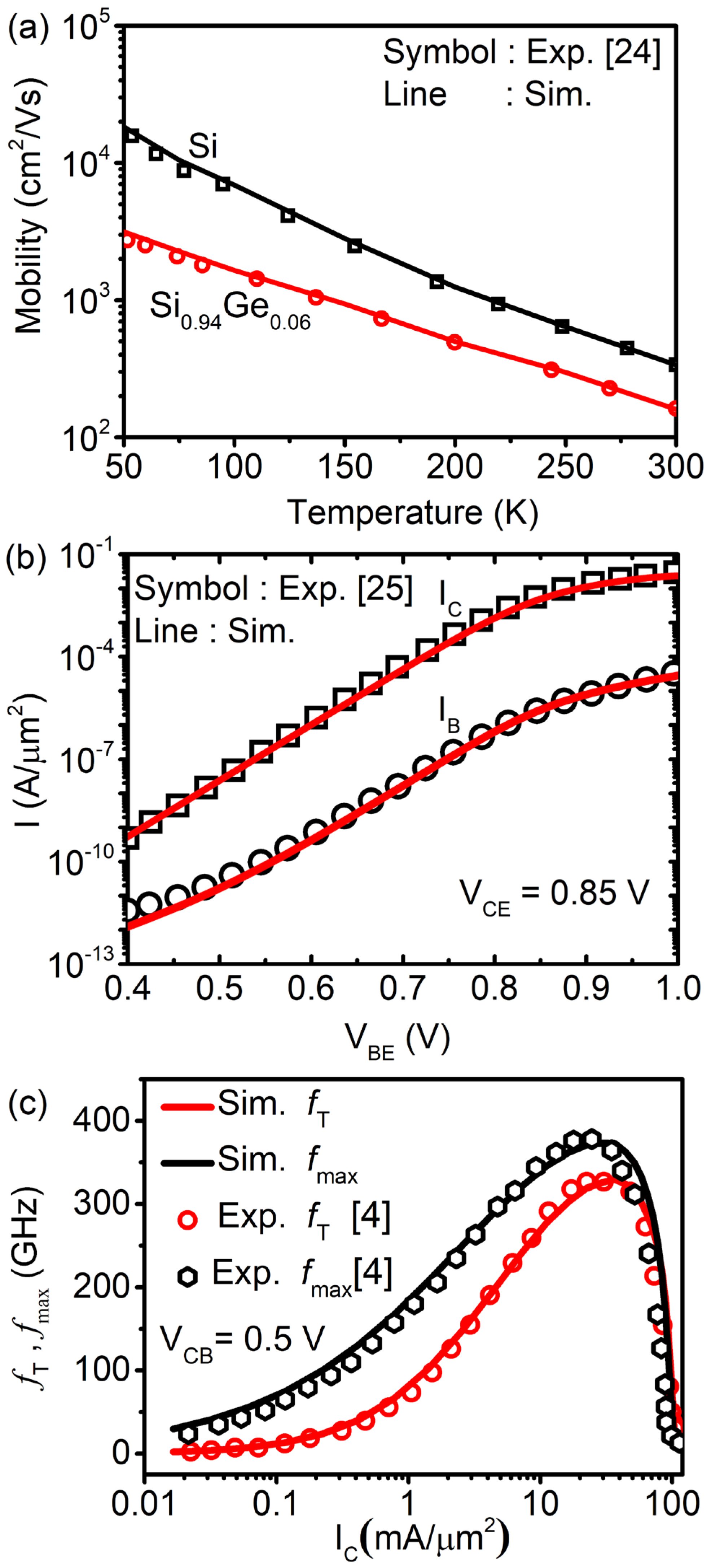
4. Effect of Reduced Ambient Temperature

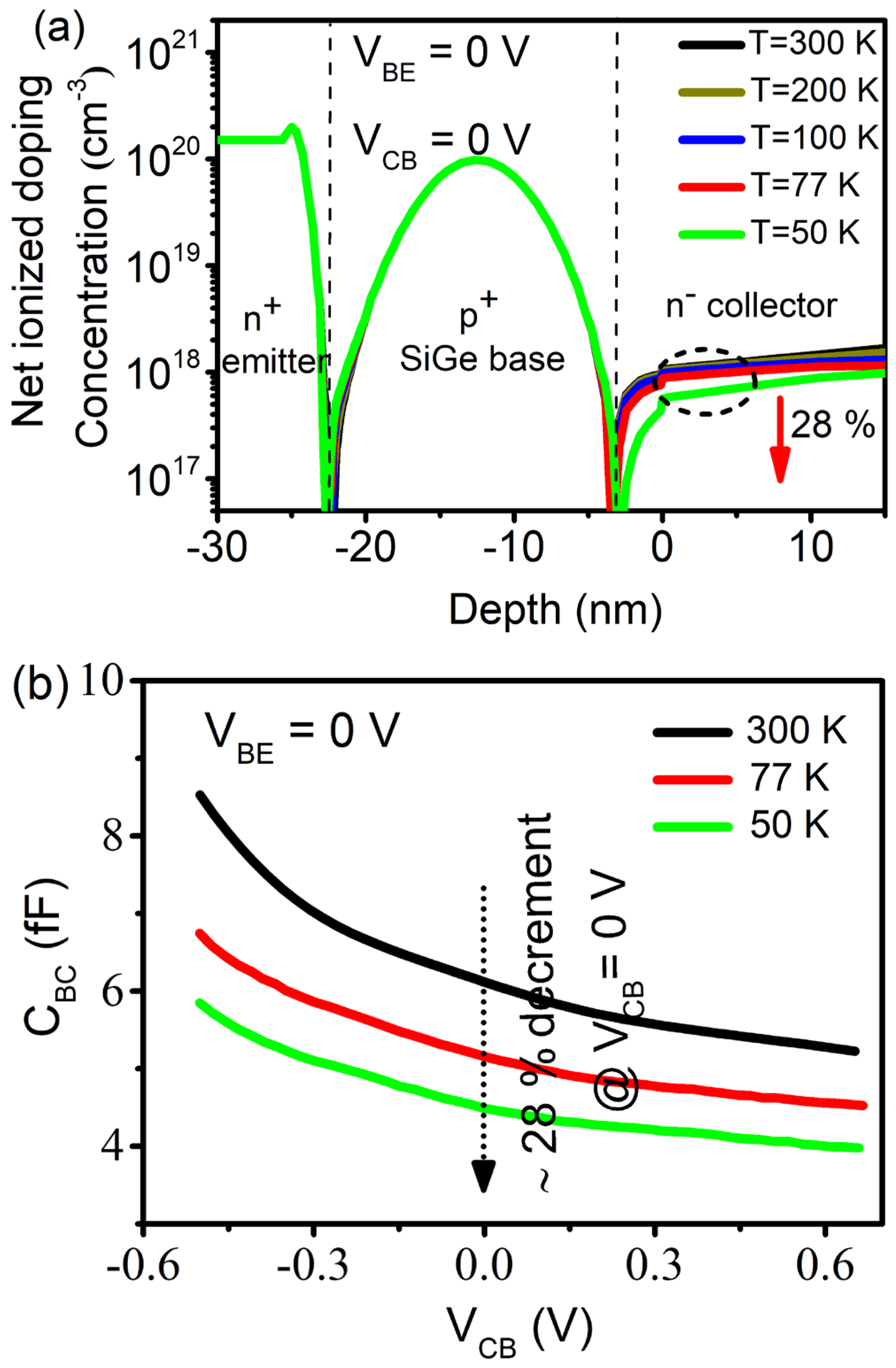
4.1. Incomplete Ionization

Under cryogenic temperatures, doping concentrations in the device below the Mott-critical concentration (NM) show incomplete dopant ionization. This incomplete ionization of dopants occurs due to the availability of insufficient thermal energy (kT; k is the Boltzmann’s constant and T is the lattice temperature) and needs to be considered [27]. From the Fermi–Dirac distribution, the ionized dopant concentration model is given by Equation (3) [14],
N D + = N D , 0 1 + g D N C , e n 0 e x p ( E D / k T )
(where, ND,0 is total dopant concentration; ND,0 < NM; gD is dopant degeneracy factor; n0 is equilibrium carrier concentration; NC,e is effective density of states; ED is dopant ionization energy). When the doping is lower as compared to the NM value, the dopant incomplete ionization is significant under cryogenic temperatures. Above the NM, dopants are fully ionized at all temperatures, considering zero dopant ionization energy in Mott-transition [6].
The NM value for arsenic (As)-doped Si is 3.5 × 1018 cm−3, and boron (B)-doped SiGe is 9.0 × 1017 cm−3, which are both considered in the analysis [27]. Here, the net doping concentration in the emitter and base regions is higher than the NM value. Therefore, all dopants in the emitter and base are fully ionized even at cryogenic temperatures, as shown in Figure 5a. However, it is observed from Figure 5a that the net ionized doping concentration in the intrinsic collector is reduced by 28% as the temperature is lowered from 300 K to 50 K. This is due to incomplete ionization of dopants in the lightly doped collector region (NC < NM) near to the CB junction. The impact of decrement in ionized dopant concentration results in a widening of the depletion width in the collector region. The incomplete ionization effect near to the junction in the lightly doped collector (<NM) region has the advantage of reducing depletion capacitance. From the simulation results, it is observed that a reduction in net ionized doping concentration due to dopant incomplete ionization at cryogenic temperatures result in an equivalent decrease in the CB depletion capacitance (CBC), as shown in Figure 5b.

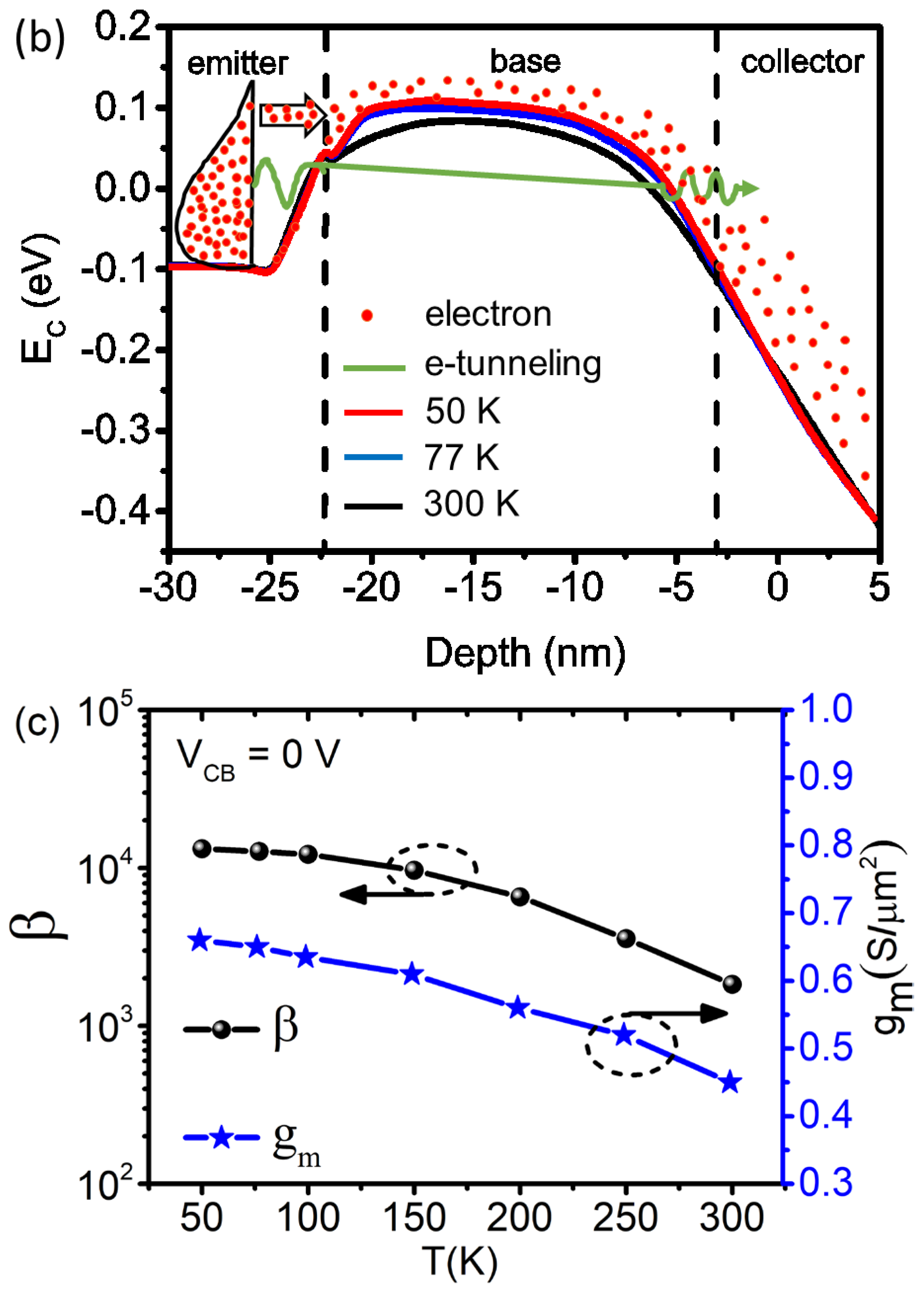
4.2. Collector Current Tunneling Leakage

An additional e-barrier tunneling model is included with hydrodynamic carrier transport to investigate electron tunneling leakage through the BE junction. This tunneling leakage current along with thermionically injected electrons constitute the IC [28]. Figure 6a shows the IC with and without e-barrier tunneling for temperatures of 300 K, 77 K, and 50 K. In the work by Ying et al. [29], it can be observed that the collector current, including the quantum mechanical tunneling model, is close to the experimental data. The effect of the inclusion of the e-barrier tunneling model can be observed in Figure 6a, where the percent increment in collector current is from 2% to 30% with the change in temperature from 300 K to 50 K. Figure 6b shows the physical illustration of the e-barrier tunneling through the base potential barrier from the emitter-base junction and contributing to IC. Under cryogenic working conditions, the intrinsic carrier concentration (ni) drops and there is an increase in the built-in potential at the junctions. Because of the increment in threshold voltage with an increase in the built-in potential, a larger VBE is required to achieve the same IC at a lower temperature [29]. Hence, at low temperatures, the barrier tunneling leakage phenomenon cannot be ignored for numerical analysis.
The IC has a strong dependency on the DC gain (β) and intrinsic transconductance (gm) of SiGe HBT. The temperature-dependent β exponentially depends on ratio E g , B E / k T   (where, E g , B E E g + E g F   ; E g is the apparent bandgap difference between base and emitter due to heterojunction, and E g F is to account for dopant induced bandgap using carrier statistics). The increase in β is due to its exponential dependence on 1/T and the enhanced diffusion of injected electrons through the graded SiGe base region into the collector. From Figure 6c, it is observed that β increases as temperature is reduced and tends to saturate at deep cryogenic temperatures. The maximum β value is estimated to be 12,500 at 50 K. The intrinsic transconductance (gm) is extracted from the derivative (dIC/dVBE) where the values of gm with respect to temperature are shown in Figure 6c. Here, it can be observed that there is an increment of gm (1.5 times) with a lowering of temperature (from 300 K to 50 K). Under cryogenic temperatures, the inclusion of the e-barrier tunneling model is important, and the comparative results shows the effect. Moreover, at lower temperatures, there is increment in gm and β, which is required to enhance device performances.

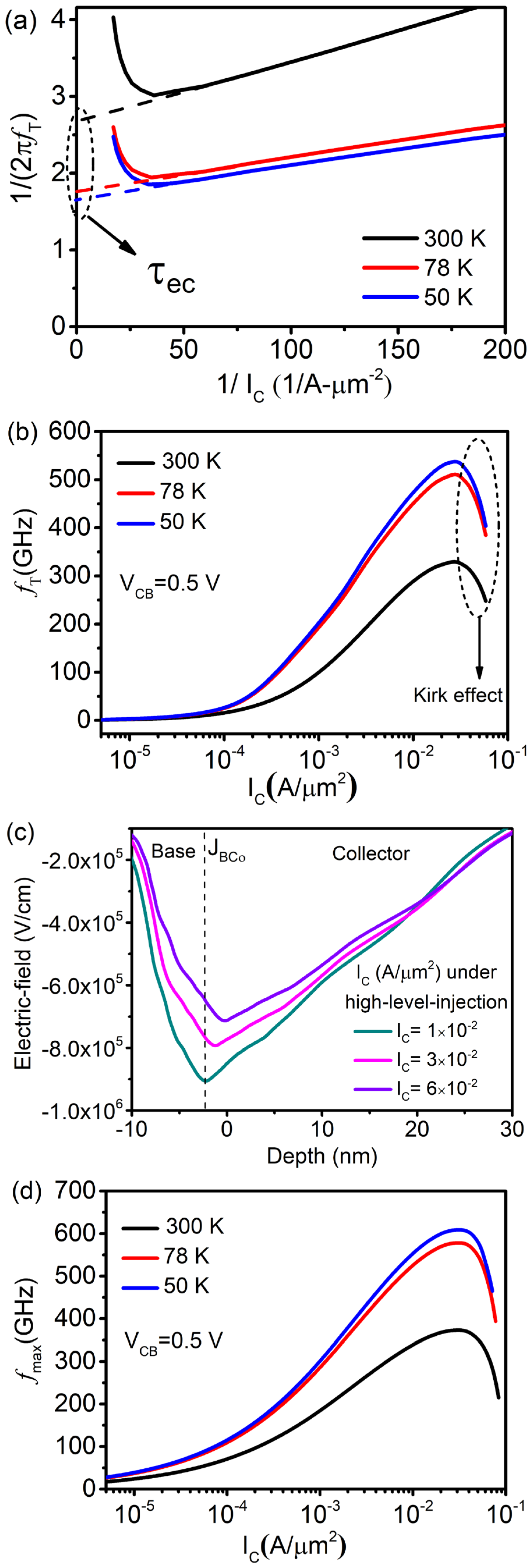
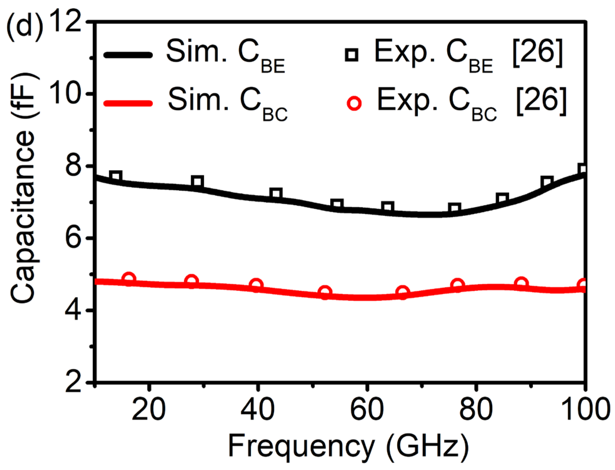
4.3. Cryogenic AC Analysis

The combined effect of cooling and the induced intrinsic drift field due to the graded Ge profile helps to reduce the emitter to collector transit time (τec), which aids in achieving high-frequency performance of transistors. The AC parameters are computed from the frequency-dependent admittance matrix [14], and the commonly used expressions for fT and fmax of bipolar transistors [30] are given by Equations (4) and (5),
1 2 π f T = τ e c + k T q I C C
f m a x = f T 8 π R B C B C
where C′ is the sum of BE and CB depletion capacitances, and RB is the sum of the distributed base resistance in the transistor. The emitter to collector transit time (τec) has an inverse relation with fT (4) that is extracted from the total delay time plot as shown in Figure 7a. Extrapolation is used to find the intersection of the curve with the 1/IC = 0 line, which results in the τec estimation. As shown in Figure 7a, τec are calculated at 300 K, 77 K, and 50 K, which shows a decrement in the τec value as the temperature is reduced. The different τec values are listed in Table 3. The peak fT is 330 GHz at 300 K and increases to 535 GHz at 50 K, as shown in Figure 7b.
In the mentioned figure, it can be observed that there is a smooth fall in the fT values, which is instigated by the high-level injection at the CB junction. This fT roll-off is due to an increase in the base transit time that increases because the base width widens; this phenomenon is called the Kirk effect [30]. During base widening, charge accumulation causes the fall of the potential gradient at the BC junction, as shown in Figure 7c, causing an increase in the total delay time of the transistor, which ultimately decreases frequencies, as shown in Figure 7b. Moreover, in the BC depletion region, space-charge modulation occurs because the injected electron density is higher than the fixed positive donor charge density [15].
The fmax of the transistor is inherently dependent on fT as presented in (5); also, under cryogenic temperatures, RB and CCB decreases increase the fmax. At low temperatures, the phonon scattering is negligible and carrier mobility inside the neutral base region is enhanced, which effectively reduces the RB and the changes in CCB is discussed in 4.1. The peak fmax increased from 375 GHz to 610 GHz with temperatures of 300 K and 50 K, respectively. The key AC performance metrics are listed in Table 3. The aggregate AC performance metric (fT + fmax) is reached in the THz regime at cryogenic temperatures. The AC performance parameters fT and fmax significantly improve at cryogenic temperatures.

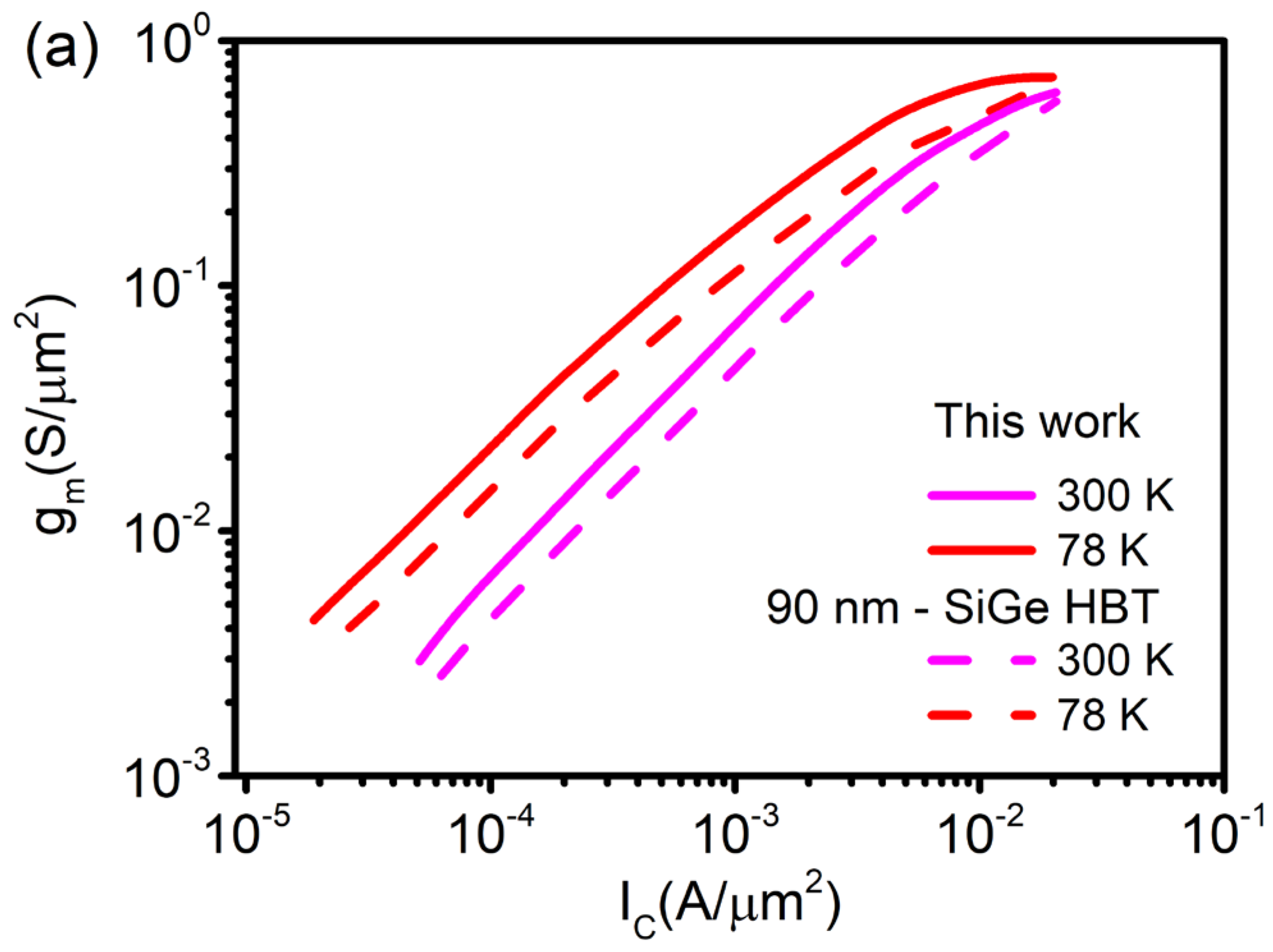
4.4. Comparison with 90 nm SiGe HBT

The simulated results are compared with commercially available data (advanced 90 nm SiGe HBT measurement at 300 K and 78 K) for performance analysis [8]. In the linear current regime, the gm increases exponentially and slows down with the high current regime; this follows the same behavior as collector current at fixed temperatures, as shown in Figure 3b. This work shows 1.5 times higher gm values with respect to the measured 90 nm SiGe HBT data (IC = 1 mA/µm2), as shown in Figure 8a. The fT analysis also shows that the simulated work is better than the measured values, as shown in Figure 8b. Even the drive current is higher in this work, which is very desirable for high performances. The IC values are (at peak fT) 2 × 10⁻² mA/µm2 in 90 nm SiGe HBT and 2.8 × 10⁻² mA/µm2 in our work. A comparison of different metrics is summarized in Table 4.

5. Conclusions

The device with assumed specifications estimates the high breakdown ability of SiGe HBT, which makes it easily integrable with Si-based CMOS. The results establish that, under cryogenic temperatures, a decrease in ionized dopant density in the lightly doped collector region is observed. A significant reduction in base-collector depletion capacitance is caused, which is useful for the fmax enhancement. In the high-field regime, e-barrier tunneling at the emitter-base junction under cryogenic temperatures is dominant. There is a significant DC gain observed in the cryogenic range and a decrement in τec and depletion capacitance, which signifies an increment in the values of fT and fmax. The peak performance (fT + fmax) reached the THz range at cryogenic temperatures, which is desirable for high-frequency device applications. The work presented here is very helpful for applications such as quantum computing, high-frequency communication, mixed-signal circuits, etc.

Author Contributions

All authors made substantial contributions to the conception and numerical device design. The data collection and analysis were performed by D.G.; the first draft of the manuscript was written by D.G.; and feedback was included after discussion with K.N. All authors have read and agreed to the published version of the manuscript.

Funding

This research received no external funding.

Institutional Review Board Statement

Not applicable.

Informed Consent Statement

Not applicable.

Data Availability Statement

Not applicable.

Conflicts of Interest

The authors declare no conflict of interest.

References

  1. Schörter, M.; Rosenbaum, T.; Chevalier, P.; Heinemann, B.; Voinigescu, S.P.; Preisler, E.; Böck, J.; Mukherjee, A. Sige hbt technology: Future trends and tcad-based roadmap. Proc. IEEE 2016, 105, 1068–1086. [Google Scholar] [CrossRef]
  2. Yuan, J.; Cressler, J.D.; Krithivasan, R.; Thrivikraman, T.; Khater, M.H.; Ahlgren, D.C.; Joseph, A.J.; Rieh, J.-S. On the performance limits of cryogenically operated sige hbts and its relation to scaling for terahertz speeds. IEEE Trans. Electron Devices 2009, 56, 1007–1019. [Google Scholar] [CrossRef]
  3. Zimmer, T.; Böck, J.; Buchali, F.; Chevalier, P.; Collisi, M.; Debaillie, B.; Deng, M.; Ferrari, P.; Fregonese, S.; Gaquiere, C.; et al. Sige hbts and bicmos technology for present and future millimeter-wave systems. IEEE J. Microw. 2021, 1, 288–298. [Google Scholar] [CrossRef]
  4. Chevalier, P.; Avenier, G.; Ribes, G.; Montagn´e, A.; Canderle, E.; Céli, D.; Derrier, N.; Deglise, C.; Durand, C.; Quémerais, T.; et al. A 55 nm triple gate oxide 9 metal layers sige bicmos technology featuring 320 ghz f t/370 ghz f max hbt and high-q millimeter-wave passives. In Proceedings of the 2014 IEEE International Electron Devices Meeting, San Francisco, CA, USA, 15–17 December 2014; IEEE: Piscataway, NJ, USA, 2014; pp. 3–9. [Google Scholar] [CrossRef]
  5. Voinigescu, S.P.; Shopov, S.; Bateman, J.; Farooq, H.; Hoffman, J.; Vasilakopoulos, K. Silicon millimeter-wave, terahertz, and high-speed fiber-optic device and benchmark circuit scaling through the 2030 itrs horizon. Proc. IEEE 2017, 105, 1087–1104. [Google Scholar] [CrossRef]
  6. Cressler, J.D.; Niu, G. Silicon-Germanium Heterojunction Bipolar Transistors; Artech House: Norwood, MA, USA, 2003. [Google Scholar]
  7. Chakraborty, P.S.; Cardoso, A.S.; Wier, B.R.; Omprakash, A.P.; Cressler, J.D.; Kaynak, M.; Tillack, B. A 0.8 thz fmax sige hbt operating at 4.3 k. IEEE Electron Device Lett. 2014, 35, 151–153. [Google Scholar] [CrossRef]
  8. Ying, H.; Teng, J.W.; Tzintzarov, G.N.; Omprakash, A.P.; Rao, S.G.; Raghunathan, U.; Ildefonso, A.; Fernandez, M.S.; Cressler, J.D. Dc and rf variability of sige hbts operating down to deep cryogenic temperatures. In Proceedings of the 2019 IEEE BiCMOS and Compound semiconductor Integrated Circuits and Technology Symposium (BCICTS), Nashville, TN, USA, 3–6 November 2019; IEEE: Piscataway, NJ, USA, 2019; pp. 1–4. [Google Scholar]
  9. Ying, H.; Wier, B.R.; Dark, J.; Lourenco, N.E.; Ge, L.; Omprakash, A.P.; Mourigal, M.; Davidovic, D.; Cressler, J.D. Operation of sige hbts down to 70 mk. IEEE Electron Device Lett. 2016, 38, 12–15. [Google Scholar] [CrossRef]
  10. Gupta, D.; Venkateswarlu, S.; Badami, O.; Nayak, K. Thz device design for sige hbt under sub-room temperature to cryogenic conditions. In Proceedings of the 5th IEEE International Conference on Emerging Electronics (ICEE), Delhi, India, 26–28 November 2020; pp. 1–4. [Google Scholar]
  11. Bonen, S.; Cooke, G.; Jager, T.; Bharadwaj, A.; Tripathi, S.P.; C´eli, D.; Chevalier, P.; Schvan, P.; Voinigescu, S.P. Cryogenic characterization of the high frequency and noise performance of sige hbts from dc to 70 ghz and down to 2 k. IEEE Microw. Wirel. Compon. Lett. 2022, 32, 696–699. [Google Scholar] [CrossRef]
  12. Braunstein, R.; Moore, A.R.; Herman, F. Intrinsic optical absorption in germanium-silicon alloys. Phys. Rev. 1958, 109, 695. [Google Scholar] [CrossRef]
  13. Varshni, Y.P. Temperature dependence of the energy gap in semiconductors. Physica 1967, 34, 149–154. [Google Scholar] [CrossRef]
  14. Sentaurus Device User Guide, Version R-2021.06-SP2; Synopsys: Mountain View, CA, USA, 2021.
  15. Ashburn, P. SiGe Heterojunction Bipolar Transistors; John Wiley & Sons: Hoboken, NJ, USA, 2004. [Google Scholar]
  16. Arienzo, M.; Iyer, S.S.; Meyerson, B.S.; Patton, G.L.; Stork, J.M. Sige alloys: Growth, properties and applications. Appl. Surf. Sci. 1991, 48, 377–386. [Google Scholar] [CrossRef]
  17. Arora, N.D.; Hauser, J.R.; Roulston, D.J. Electron and hole mobilities in silicon as a function of concentration and temperature. IEEE Trans. Electron Devices 1982, 29, 292–295. [Google Scholar] [CrossRef]
  18. Lombardi, C.; Manzini, S.; Saporito, A.; Vanzi, M. A physically based mobility model for numerical simulation of nonplanar devices. IEEE Trans. Comput. Aided Des. Integr. Circuits Syst. 1988, 7, 1164–1171. [Google Scholar] [CrossRef]
  19. Klaassen, D. A unified mobility model for device simulation-ii. temperature dependence of carrier mobility and lifetime. Solid-State Electron. 1992, 35, 961–967. [Google Scholar] [CrossRef]
  20. Choo, S.C. Theory of a forward-biased diffused-junction pln rectifier|part i: Exact numerical solutions. IEEE Trans. Electron Devices 1972, 19, 954–966. [Google Scholar] [CrossRef]
  21. Stratton, R. Diffusion of hot and cold electrons in semiconductor barriers. Phys. Rev. 1962, 126, 2002. [Google Scholar] [CrossRef]
  22. Altermatt, P.; Schenk, A.; Heiser, G. A simulation model for the density of states and for incomplete ionization in crystalline silicon. i.establishing the model in si: P. J. Appl. Phys. 2006, 100, 113715. [Google Scholar] [CrossRef]
  23. Ying, H.; Teng, J.W.; Raghunathan, U.S.; Moody, J.P.; Cressler, J.D. Variability of pn junctions and sige hbts at cryogenic temperatures. IEEE Trans. Electron Devices 2021, 68, 2021. [Google Scholar] [CrossRef]
  24. Gaworzewski, P.; Tittelbach-Helmrich, K.; Penner, U.; Abrosimov, N. Electrical properties of lightly doped p-type silicon{germanium single crystals. J. Appl. Phys. 1998, 83, 5258–5263. [Google Scholar] [CrossRef]
  25. Puglisi, F.M.; Larcher, L.; Pavan, P. Mixed-mode stress in silicon-germanium heterostructure bipolar transistors: Insights from experiments and simulations. IEEE Trans. Device Mater. Reliab. 2019, 19, 275–282. [Google Scholar] [CrossRef]
  26. Deng, M.; Qu´emerais, T.; Bouvot, S.; Gloria, D.; Chevalier, P.; L’epilliet, S.; Danneville, F.; Dambrine, G. Small-signal characterization and modelling of 55 nm sige bicmos hbt up to 325 ghz. Solid-State Electron. 2017, 129, 150–156. [Google Scholar] [CrossRef]
  27. Moen, K.A.; Cressler, J.D. Measurement and modeling of carrier transport parameters applicable to sige bicmos technology operating in extreme environments. IEEE Trans. Electron Devices 2010, 57, 551–561. [Google Scholar] [CrossRef]
  28. Cressler, J.D. Silicon-germanium as an enabling technology for extreme environment electronics. IEEE Trans. Device Mater. Reliab. 2010, 10, 437–448. [Google Scholar] [CrossRef]
  29. Ying, H.; Dark, J.; Omprakash, A.P.; Wier, B.R.; Ge, L.; Raghunathan, U.; Lourenco, N.E.; Fleetwood, Z.E.; Mourigal, M.; Davidovic, D.; et al. Collector transport in sige hbts operating at cryogenic temperatures. IEEE Trans. Electron Devices 2018, 65, 3697–3703. [Google Scholar] [CrossRef]
  30. Taur, Y.; Ning, T.H. Fundamentals of Modern VLSI Devices; Cambridge University Press: Cambridge, UK, 2021. [Google Scholar]
Figure 1. (a) The analytical model (1) calibrated at different Ge mole fractions with experimental data [15]; (b) for the wide range of temperature, the computed expression observed closely matched with measurement data [12].
Electronics 11 04164 g001
Figure 2. (a) A simplified 2-D schematic cross-sectional view of SiGe HBT structure; (b) Shows net doping concentration of the device intrinsic region and linearly graded germanium profile (5% at the EB junction and 23% at the CB junction); (c) equilibrium energy band diagram of n−p−n SiGe HBT with Ge profile.
Electronics 11 04164 g002
Figure 3. Calibration: (a) Phu−Mob model with experimental data [24]; (b) forward Gummel characteristics with experimental data [25]; (c) fT and fmax at VCB = 0.5 V with experimental data [4]; (d) emitter-base (CBE) and collector−base (CBC) junction capacitances with measurement data [26].
Electronics 11 04164 g003aElectronics 11 04164 g003b
Figure 4. (a) The HBT is biased at VBE = 0.7 V, and −IB is the absolute value of the CB junction avalanche produced due to the impact-ionization hole current. +IB is the positive base current fueled by a forward-biased BE junction; (b) impact−ionization base current reversal (IB) and avalanche multiplication factor (M−1) vs. VCB.
Electronics 11 04164 g004
Figure 5. (a) Dopant incomplete ionization increases (net ionized doping concentration reduces) in the lightly doped (<NM) intrinsic collector region with decreasing temperatures; (b) collector−base depletion capacitance (CBC) in the lightly doped collector region decreased with an equivalent amount of decrease in doping concentration at VBE = VCB = 0 V under cryogenic temperature.
Electronics 11 04164 g005
Figure 6. (a) IC—VBE characteristics with (solid line) and without (dotted line) barrier tunneling leakage; (b) conduction band edge energy (EC) vs. depth for the intrinsic HBT, the theoretical prediction of e−barrier tunneling from the BE junction into the base contributing to collector current leakage; and (c) DC gain (β) and transconductance (gm) vs. temperature (T).
Electronics 11 04164 g006aElectronics 11 04164 g006b
Figure 7. (a) Total delay time travel by the minority charge carrier ( 1 / 2 π f T ) vs. 1/IC. The τec is extracted with extrapolation of the linear part intersecting at 1/IC = 0; (b) fT (GHz) vs. IC (A/µm2); (c) electric−field profile at the CB junction at high IC; and (d) fmax (GHz) vs. IC (A/µm2).
Electronics 11 04164 g007
Figure 8. (a) The gm vs. IC at VCB = 0 V; (b) the peak fT is comparatively larger in this work with respect to 90 nm SiGe HBT measurement data [8].
Electronics 11 04164 g008aElectronics 11 04164 g008b
Table 1. Energy bandgap model parameter [14].
ParameterFor SiFor Ge
α (eV/K)4.73 × 10−44.80 × 10−4
β (K)636235
Eg(0) (eV)1.170.742
Table 2. Numerical Device Simulation Parameters.
ParameterValue
Device Dimension
Emitter window width (WE) 0.1 µm
Emitter base spacer width (WSP)25 nm
Effective vertical base width (wb)∼19 nm
Peak emitter doping (NEp)1.5 × 1020 cm3
Peak intrinsic base doping (NBi)9.9 × 1019 cm3
Extrinsic base doping (NB)1.0 × 1020 cm3
Collector doping (min) (Nc)3 × 1017 cm3
Collector doping (max) (NC)1.5 × 1020 cm3
Calibrated Model Parameters
Incomplete ionization model
NM (Si)3.5 × 1018 cm3
gD (Si)2
NM (SiGe)9.0 × 1017 cm3
gD (SiGe)4
Philips unified mobility (PhU-Mob) model
µmax (e), µmax (h) 2.036 × 10³, 9.154 × 10² (cm2/V·s)
µmin (e), µmin (h) 69.15, 58.675 (cm2/V·s)
θ (e), θ (h) 2.1, 2.2
Nref (e), Nref (h)1.476 × 10¹⁷, 2.673 × 10¹⁷ (cm3)
Table 3. The AC performance metrics of SiGe HBT.
Parameter/Temperature300 K78 K50 K
Peak fmax (GHz)375580610
Peak fT (GHz)330510535
τec (ps)2.671.761.63
Table 4. The advanced SiGe HBTs figure-of-merit comparison.
ParameterThis Work90 nm SiGe HBT
300 K78 K300 K78 K
Peak fT (GHz)330510315467
Peak β183012,2005661013
gm(S/µm2) @ IC (=1 mA/µm2)0.070.170.050.12
Publisher’s Note: MDPI stays neutral with regard to jurisdictional claims in published maps and institutional affiliations.

