Abstract
With the advantages of lower capacitance, faster operation and smaller size, the amorphous silicon antifuse is very promising for high-speed and high-density FPGA. However, the leakage current of the conventional amorphous silicon antifuse in the off-state is high, which decreases its performance and reliability. Although the leakage current of the SiNX or SiOX antifuse is small, the proper thickness of the dielectric layer is not easily controlled by PECVD processes. In addition, the highly undesirable switch-off behavior is common to almost all metal-to-metal antifuse structures. Focusing on the study of amorphous silicon multilayer dielectric structures, a novel antifuse with the structure of Al/α-Si:H,N/α-Si:H/Al was proposed, which was manufactured by nitrogen plasma treatment for an α-Si:H film surface. Through surface plasma treatment, the hydrogen content of the dielectric layer is stable, the film surface is smoother, the leakage current is reduced, the switch-off behavior is eliminated, the programming voltage is more concentrated and the on-state resistance distribution is more compact. The results demonstrated that surface plasma treatment with proper time for the dielectric layer could significantly improve the performance and reliability of the Al/α-Si:H,N/α-Si:H/Al antifuse. Furthermore, the fabrication process of the α-Si:H,N/α-Si:H structure has excellent compatibility, controllability and simplicity.
1. Introduction
Antifuse has been extensively employed in Field Programmable Gate Arrays (FPGA) as a programmable link [1,2,3,4,5,6]. FPGA typically consists of three components: programmable logic blocks, programmable routing, and I/O blocks. Among the three, the programmable routing interconnect comprises almost 90% of the total chip area and thus contributes to most of the delay, area and power consumption [6]. Typically, an FPGA uses 20 to over 100 interconnects per logic gate to link logic blocks [6]. Antifuses are among the commonly used interconnect devices for FPGAs. In contrast to EEPROM and SRAM memory cells used for programmable interconnect devices, the antifuse has higher reliability, more quick access time, and smaller size. The antifuse is a one-time programmable (OTP) cell, and it consists of two electrodes and a thin dielectric film as the insulating layer sandwiched between them. Typical antifuses include oxide-nitride-oxide (ONO), amorphous silicon (α-Si:H) and gate oxide structures [7,8,9,10]. Antifuses are programmed from a high resistance or off-state to a low resistance or on-state by applying a voltage or current pulse across the electrodes.
A reliable antifuse device requires a very high resistance or low leakage current in the off-state before programming and a permanent low resistance in the on-state after programming. For ONO antifuse, it has a n+ diffusion/oxide–nitride−oxide/polysilicon structure; although the three-layer dielectric structure could reduce its leakage current, it needs to be thinned down to keep the programming voltage below acceptable limits, which leads to high capacitance of the antifuse [7,11].
For gate oxide antifuse, although it is implemented in a standard foundry CMOS logic process, its programmed resistance varies with the breakdown position along the channel. The low programmed resistance of about several hundred ohms occurs in a breakdown spot located over the source-drain extension regions, and great programmed resistance of about tens of kilohms occurs in a breakdown spot located away from the source–drain extension regions [12,13]. Furthermore, the breakdown spot occurs randomly, which could not be precisely controlled. In addition, the programmed resistance is independent of the channel length. The uncertainty of the programmed resistance value due to the breakdown-position uncertainty leads to inconsistent signal delay (RC delay) time, which results in poor performance for high-speed FPGA. Therefore, with gate oxide antifuse used as programmable interconnect device, high-performance FPGA cannot be realized.
For α-Si:H antifuse, which is called metal-to-metal antifuse, it has a structure consisting of a hydrogenated amorphous silicon dielectric layer sandwiched between two metal electrodes. With the advantages of lower capacitance, faster operation and smaller size, α-Si:H antifuse is very promising for high-speed and high-density FPGA [14].
However, the leakage current of α-Si:H antifuse in the off-state is high, which decreases its performance and reliability. For metal-to-metal antifuses with other dielectric layers such as silicon nitride (SiNX), silicon oxide (SiOX) and nitride-oxide (NO), their leakage currents are very low. The leakage current density at the voltage of 5.5 V is below 10−12 A/μm2 for NO antifuse, about 10−14 to 10−13 A/μm2 for SiNX or SiOX antifuse, and about 10−9 A/μm2 for α-Si:H antifuse [15,16,17,18]. Furthermore, the thickness of the dielectric layer must be controlled tightly since it affects the programming voltage. To achieve 8–10 V programming voltage, the thicknesses of different dielectric layers are different. NO is the composite of 7 nm nitride and 3.5 nm oxide; the thicknesses of SiNX, SiOX and α-Si:H dielectric layers are about 10 nm, 6 nm, and 60 nm, respectively. For a metal-to-metal antifuse structure, the dielectric layer is usually prepared by plasma-enhanced chemical vapor deposition (PECVD) processes. However, the proper thickness of the dielectric layer is not easily controlled by PECVD processes; the average deposition rate is about 1–2 nm/s for SiNX or SiOX, and 0.5–1 nm/s for α-Si:H, respectively. Thus, the thicker α-Si:H layer is easier to be deposited and be scaled down than the thinner layers required for NO, SiNX and SiOX antifuses. To decrease the leakage current of α-Si:H antifuse, SiNX or SiOX thin film can be deposited on the α-Si:H layer to obtain multilayered dielectric antifuse, which is similar with the NO antifuse. However, as a thin layer of multilayered dielectric, it is even more difficult to control the proper thickness for very thin SiNX or SiOX film. On the one hand, if its thickness is not thick enough, the leakage current will not decrease obviously. On the other hand, if its thickness is over thick, the programming voltage will exceed acceptable limits.
Most of the existing metal-to-metal antifuses show very good off-state reliability; however, their on-state reliability is still an area of concern [19]. It was found that an amorphous silicon antifuse, once programmed, can switch back to the off-state during later operation. This kind of on-off switching behavior, which was called switch-off, has also been observed for the SiOX, SiNX, NO and AlN-based metal-to-metal antifuse [1,4,7,16,19,20,21]. Switch-off is highly undesirable, as it results in the failure of the antifuse device.
The mature and commercialized state-of-art antifuse FPGAs are all based on metal-to-metal antifuses. Microsemi’s antifuse consists of a two-layer dielectric composed of silicon nitride and amorphous silicon sandwiched between a raised tungsten plug and the top metal layer. The QuickLogic antifuse structure consists of two metal layers separated by a single layer amorphous silicon dielectric. In the literature [7], it is found that in the reliability test, the two types of FPGAs all have some individual phenomena of programming failure. The standby current of the antifuse FPGA product can reach 8 mA due to the antifuse leakage [18].
Surface treatment by plasma is one method to improve properties of semiconductor materials. A very thin film of α-Si:H,N could be formed on the α-Si:H film which has had surface treatment conducted by nitrogen plasma. Thus, the multilayered dielectric antifuse, α-Si:H,N/α-Si:H antifuse, could have low leakage current and improved reliability.
Fundamental research on α-Si:H antifuse with surface treatment by nitrogen plasma is quite scarce. In this paper, the amorphous silicon dielectric layer received surface treatment conducted by nitrogen plasma. The effect of the dielectric layer with nitrogen plasma treatment on the characteristics of α-Si:H antifuse with a metal-to-metal structure was investigated.
2. Experimental
Figure 1a illustrates the newly developed antifuse with the structure of Al/α-Si:H,N/α-Si:H/Al, and Figure 1b shows the fabrication process flows of the Al/α-Si:H,N/α-Si:H/Al antifuse.
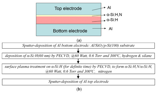
Figure 1.
The structure and process-flowchart of the Al/α-Si:H,N/α-Si:H/Al antifuse (the antifuse area is 314 μm2): (a) schematic cross-section, (b) process flowchart.
The hydrogenated amorphous silicon thin film was prepared on Al/SiO2/p-Si(100) substrate by PECVD processes. The radio frequency (RF) power, total pressure and substrate temperature were 60 Watt, 0.6 Torr and 300 °C, respectively. After the deposition of α-Si:H, surface treatment was conducted by PECVD under the same conditions as those of α-Si:H deposition with the gas of nitrogen instead of silane. The thickness of the α-Si:H thin film was about 60 nm, which was estimated and controlled by the growth rate. After these processes, Al top dot electrodes with a diameter of 20 μm were deposited by means of sputtering using a shadow mask. Serial antifuse samples were manufactured with the dielectric films treated by nitrogen plasma for different times: the Al/α-Si:H,N/α-Si:H/Al (N-2min) antifuse with 2 min treatment, the Al/α-Si:H,N/α-Si:H/Al (N-5min) antifuse with 5 min treatment, and the Al/α-Si:H,N/α-Si:H/Al (N-10min) antifuse with 10 min treatment. For comparison, Al/α-Si:H/Al antifuse with the same thickness of dielectric layer was also manufactured.
The hydrogen contents of α-Si:H and α-Si:H,N/α-Si:H thin films were determined using a Nicolet 6700 Fourier transform infrared spectrometer (FTIR) in specular reflectance sampling mode. The surface morphologies were investigated using a SPA-300 HV atomic force microscope (AFM). The electrical characteristics of the antifuses were investigated with a HP 4155B semiconductor parameter analyzer. The I–V curves were measured under a linear sweep bias with 0.05 V/step from 0 up to its breakdown voltage.
3. Results and Discussion
3.1. Hydrogen Content of the Amorphous Silicon Thin Films
The α-Si:H thin film is the important dielectric material for amorphous silicon antifuse. Surface plasma treatment was made on α-Si:H thin film with basic qualified characteristics. In order to detect whether the α-Si:H film had qualified characteristics, the hydrogen content was calculated from the infrared (IR) transmission curves measured by the FTIR spectrometer, which was directly related to characteristics of α-Si:H thin film. Simultaneously, to detect the influence of plasma treatment on the film material, the hydrogen content of α-Si:H,N/α-Si:H thin film was also estimated.
Figure 2 illustrates the FTIR spectra of α-Si:H thin film and α-Si:H,N/α-Si:H (N-5min) thin film with nitrogen plasma treatment for 5 min. Usually, there are many defects in amorphous silicon, which leads to poor performance and reliability for amorphous silicon antifuse. These defects come from dangling bonds of Si-. For hydrogenated amorphous silicon, hydrogen in a proper amount can saturate silicon dangling bonds to significantly decrease defects. Therefore, to manufacture α-Si:H antifuse with stable performance, the α-Si:H thin film should have proper hydrogen content.
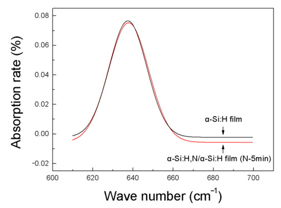
Figure 2.
FTIR spectra of the α-Si:H and α-Si:H,N/α-Si:H (N-5min) thin films.
The vibrational spectrum of hydrogenated amorphous silicon contains wagging, bending, and stretching modes. The absorption band near 640 cm−1 is attributed to the wagging or rocking mode. The amount of bonded hydrogen, CH, can be calculated by numerical integration of the Si-H wagging-rocking mode at 640 cm−1 using the expression as below [22,23].
where A640 = 2.1 × 1019 cm−2 is the proportionality coefficient, α is the absorption coefficient, and ω is the frequency.
The hydrogen content in the prepared α-Si:H thin film was 10.3%, which is calculated from Figure 2. The preferred hydrogen content is about 10% in α-Si:H, which can result in a functional antifuse [24,25]. There was no obvious difference for the hydrogen contents of α-Si:H thin films with surface plasma treatment for different times. The α-Si:H,N/α-Si:H (N-5min) thin film had the similar hydrogen content (10.1%) with α-Si:H thin film. Therefore, the α-Si:H thin film conducted the subsequent surface plasma treatment had basic qualified characteristics, and the surface plasma treatment did not significantly affect the characteristics of the bulk of α-Si:H thin film material; it only affected a very thin surface area in the thickness direction of the film.
3.2. Surface Morphologies of the Amorphous Silicon Thin Films
Figure 3 shows the AFM surface morphologies of the α-Si:H and α-Si:H,N/α-Si:H (N-5min) thin films. A dense microstructure without any crack was obtained. It could be seen that the α-Si:H thin film was mainly composed of irregular grains with the rms (root mean square) roughness about 3.35 nm, and the α-Si:H,N/α-Si:H thin film was mainly composed of fine grains with the rms roughness about 2.24 nm.
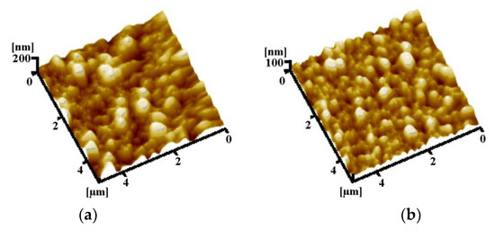
Figure 3.
AFM surface morphologies: (a) the α-Si:H thin film and (b) the α-Si:H,N/α-Si:H (N-5min) thin film.
3.3. Current–Voltage Characteristics of the Amorphous Silicon Antifuses
Figure 4a shows typical I–V curves of the Al/α-Si:H/Al and Al/α-Si:H,N/α-Si:H/Al serial antifuses. The maximum current in the semiconductor parameter analyzer was limited to 10 mA to simulate the programming current in actual application and prevent the instrument from being damaged by overcurrent after the breakdown of the antifuse. Figure 4a illustrates the results before and after breakdown, respectively. The I–V curves of the newly developed Al/α-Si:H,N/α-Si:H/Al(N-5min) antifuse are shown in Figure 4b, which illustrates the statistics properties of the newly developed antifuse.
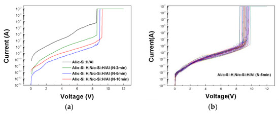
Figure 4.
I–V curves: (a) the Al/α-Si:H/Al antifuse and Al/α-Si:H,N/α-Si:H/Al serial antifuses with dielectric films treated by nitrogen plasma for different time; (b) the statistics properties of Al/α-Si:H,N/α-Si:H/Al (N-5min) antifuse with dielectric films treated by nitrogen plasma for 5 min.
The leakage current increased monotonously with increasing voltage; then, the current increased sharply to the current limit at the breakdown voltage. During the process of breakdown, the conductive filament was formed in the antifuse device at high applied voltage/current. The power used to form conductive filament was to be high enough to produce sufficient Joule heating during the forming process [20,26]. Before breakdown, the leakage currents of Al/α-Si:H,N/α-Si:H/Al serial antifuses were far lower than those of Al/α-Si:H/Al antifuse at the same voltage. The leakage current of Al/α-Si:H/Al antifuse was about 10−7 A at 5 V, whereas that of Al/α-Si:H,N/α-Si:H/Al (N-5min) antifuse was only 10−10 A at the same voltage, decreasing by three orders of magnitude. The breakdown voltage of Al/α-Si:H,N/α-Si:H/Al antifuse increased about only 0.5 V. Thus, nitrogen plasma treatment could significantly improve the performance and reliability of the amorphous silicon antifuse by decreasing its leakage current, but it did not significantly increase the programming voltage over acceptable limits. There were two reasons why surface plasma treatment on the dielectric film could decrease the leakage current of the amorphous silicon antifuse. On the one hand, nitrogen plasma treatment could further saturate silicon dangling bonds of the surface, as hydrogen could not completely saturate silicon dangling bonds. Then, the defects of the α-Si:H thin film decreased furthermore, resulting in low leakage current for the antifuse. On the other hand, the multilayered dielectric film (α-Si:H,N/α-Si:H) was formed after the α-Si:H film was treated by surface nitrogen plasma. The leakage current pathway was changed in the multilayered dielectric film, resulting in low leakage current for Al/α-Si:H,N/α-Si:H/Al antifuse. Simultaneously, the multilayered dielectric film with an additional very thin film of α-Si:H,N caused a slight increase in the programming voltage for Al/α-Si:H,N/α-Si:H/Al antifuse. The result of the slight increase in the programming voltage was consistent with that of hydrogen content analysis from the FTIR spectra; the surface plasma treatment only affected a very thin area in the thickness direction of the film.
The leakage currents and the programming voltages as the functions of the time of surface plasma treatment are also shown in Figure 4a. The leakage current of the Al/α-Si:H,N/α-Si:H/Al serial antifuses apparently decreased and reached the minimum with the time of surface plasma treatment being increased up to 5 min; then, it increased with the time of surface plasma treatment being further increased. The leakage currents at 5 V were about 10−8 A, 10−10 A, and 10−9 A for Al/α-Si:H,N/α-Si:H/Al (N-2min), Al/α-Si:H,N/α-Si:H/Al (N-5min), and Al/α-Si:H,N/α-Si:H/Al (N-10min) antifuses, respectively. The programming voltages increased monotonously and slightly with the time of surface plasma treatment being increased. The programming voltages were about 8.6 V, 9 V, and 9.2 V for Al/α-Si:H,N/α-Si:H/Al (N-2min), Al/α-Si:H,N/α-Si:H/Al (N-5min), and Al/α-Si:H,N/α-Si:H/Al (N-10min) antifuses. respectively, which were all under acceptable limits. With the time of surface plasma treatment for dielectric films being increased, nitrogen plasma could saturate more silicon dangling bonds of the surface, and the defects of the surface decreased gradually, resulting in a gradual decrease in the leakage current for the Al/α-Si:H,N/α-Si:H/Al antifuse. When the time of surface plasma treatment was increased to 5 min, the saturation of the surface dangling bonds was maximized, and there was the minimum number of surface defects, resulting in the lowest leakage current for Al/α-Si:H,N/α-Si:H/Al (N-5min) antifuse. When the time of surface plasma treatment continued to be increased, nitrogen plasma could not further saturate the silicon dangling bonds of the surface; on the contrary, it would cause the etching effect. The surface defects increased again due to the plasma etching on the surface. The leakage current increased again for Al/α-Si:H,N/α-Si:H/Al (N-10min) antifuse. Therefore, plasma treatment with proper time for the dielectric film could greatly decrease the leakage current for Al/α-Si:H,N/α-Si:H/Al antifuse.
3.4. Switch-off Behavior of the Amorphous Silicon Antifuses
The typical I–V characteristics of the programmed Al/α-Si:H/Al and Al/α-Si:H,N/α-Si:H/Al (N-5min) antifuses are shown in Figure 5. After programming, the antifuses exhibited linear ohmic characteristic. The programmed antifuses had very low resistances of less than 50 Ω. Then, the maximum current limit was increased to three times the programming current; when the voltage exceeded a certain voltage value, a transition was made to a higher resistance state for the programmed Al/α-Si:H/Al antifuse, which was called switch-off, as shown in Figure 5a [19,21]. However, switch-off did not occur for the programmed Al/α-Si:H,N/α-Si:H/Al (N-5min) antifuse, and it still exhibited a linear ohmic characteristic, with a little lower resistance (about 24 Ω), as shown in Figure 5b. The Al/α-Si:H,N/α-Si:H/Al (N-5min) antifuse showed high reliability after programming.
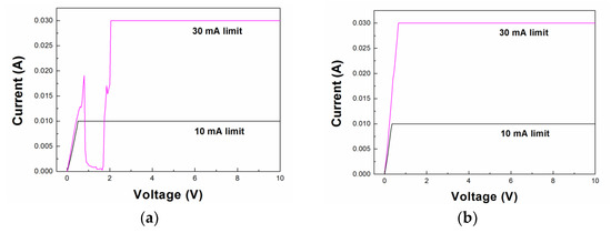
Figure 5.
I–V characteristics of the programmed antifuses: (a) the Al/α-Si:H/Al antifuse and (b) the Al/α-Si:H,N/α-Si:H/Al (N-5min) antifuse.
The reliability of the programmed Al/α-Si:H/Al and Al/α-Si:H,N/α-Si:H/Al (N-5min) antifuses was related to surface morphologies of the α-Si:H and α-Si:H,N/α-Si:H dielectric films, which are shown in Figure 3. The fine surface of the α-Si:H,N/α-Si:H thin film could improve the interface characteristics for the Al/α-Si:H,N/α-Si:H/Al antifuse. The local electric field concentration was not serious for the Al/α-Si:H,N/α-Si:H/Al antifuse under the same applied voltage. The concentrated local electric field was more likely to cause switch-off occurring in the programmed Al/α-Si:H/Al antifuse.
3.5. On-State Resistance Distribution of the Amorphous Silicon Antifuses
After the antifuses were programmed, the resistance distribution and the cumulative distribution of on-state resistance for the programmed Al/α-Si:H/Al and Al/α-Si:H,N/α-Si:H/Al (N-5min) antifuses are shown in Figure 6. The programmed Al/α-Si:H/Al antifuses exhibited an average resistance distribution in the range of 10 to 90 ohms; however, the programmed Al/α-Si:H,N/α-Si:H/Al antifuses exhibited a tight resistance distribution in the range of 10 to 60 ohms with about 54% being concentrated in the range of 30 to 40 ohms. The results showed that the programmed characteristic of Al/α-Si:H,N/α-Si:H/Al antifuses was better than that of Al/α-Si:H/Al antifuses.
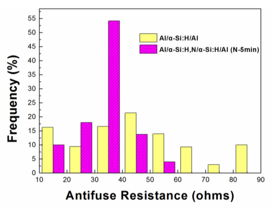
Figure 6.
Resistance distribution for the programmed Al/α-Si:H/Al and Al/α-Si:H,N/α-Si:H/Al (N-5min) antifuses.
The resistance distribution of the programmed Al/α-Si:H/Al and Al/α-Si:H,N/α-Si:H/Al (N-5min) antifuses was also related to surface morphologies of the α-Si:H and α-Si:H,N/α-Si:H dielectric films. The fine surface of the α-Si:H,N/α-Si:H film caused the uniform electric field for the Al/α-Si:H,N/α-Si:H/Al antifuse, resulting in the tight distribution for the programmed resistances. For the Al/α-Si:H/Al antifuse, the rough surface of the α-Si:H film caused the uneven electric field with or without local field concentration, resulting in the distribution over a wide range for the programmed resistances.
3.6. Experimental Data Comparison of Different Dielectric/α-Si Structures
In addition to the α-Si:H,N/α-Si:H structure that has been evaluated above, the other resemble dielectric/α-Si structures have similar characteristics. Table 1 gives a quantitative comparison of the characteristics of different structures, in which the thickness of each dielectric layer was given, respectively. The results listed in Table 1 are all stable and repeatable by experiments. Every dielectric/α-Si experimental sample in Table I had the same area of 314 μm2.

Table 1.
The characteristics of different dielectric/α-Si structures.
As shown in Table 1, the off-state leakage current of the SiNX/α-Si:H structure was obviously larger than that of the α-Si:H,N/α-Si:H (N-5min) structure at 5 V. However, although the off-state leakage current of the SiNX/α-Si:H/SiNX structure or SiOX/α-Si:H structure was lower or far lower than that of the α-Si:H,N/α-Si:H (N-5min) structure at 5 V, the maximum programming voltage of the former, up to 20 V above, was significantly larger than the latter. Furthermore, the programming voltage value of the SiNX/α-Si:H/SiNX structure was more discrete than that of the α-Si:H,N/α-Si:H (N-5min) structure. In addition, the α-Si:H,N/α-Si:H structure, especially the α-Si:H,N/α-Si:H (N-5min), has the smallest on-state resistance compared to the other resemble dielectric/α-Si structures in Table 1.
As the scale of the antifuse FPGA circuit increases, the size of the CMOS device, especially the high-voltage device of the programming circuit, needs to be reduced as much as possible for the high-density antifuse FPGA. However, the withstand voltage of small-size CMOS devices is limited, so it is necessary to limit the programming voltage of the antifuse, such as 8 to 10 V. The experimental data in Table 1 show that the α-Si:H,N/α-Si:H (N-5min) structure was the best choice for taking into account the small off-state leakage current, low on-state resistance and limited programming voltage. Furthermore, the fabrication process of the α-Si:H,N/α-Si:H (N-5min) structure has better compatibility, controllability and simplicity compared to other resemble dielectric/α-Si structures in Table 1.
3.7. Comparison of Different Dielectric Antifuses
The comparison between the previous works and the current work is shown in Table 2.
Table 2.
The comparison between the previous works and the current work.
As can be seen from Table 2, the positive significance of the newly developed α-Si:H,N/α-Si:H antifuse has the following aspects.
(1) The α-Si:H,N/α-Si:H antifuse in Table 2 has the highest reliability due to its elimination of the switch-off effect.
(2) To achieve ideal programming voltage (8–10 V), the film thickness of SiNX, SiOX, or NO, too thin, is difficult to achieve stable control by PECVD processes, but the thicker thickness (60 nm/80 nm) of the α-Si film is easy to be deposited stably. So, the α-Si film is an ideal choice for fabricating the antifuse.
(3) The off-state leakage of the α-Si:H,N/α-Si:H antifuse is very low, close to that of SiNX and SiOX, and significantly better than the α-Si:H.
(4) The on-state resistance of the α-Si:H,N/α-Si:H antifuse is small and tight, close to that of SiNX and SiOX, and better than the α-Si:H.
(5) The programming voltage distribution of the α-Si:H,N/α-Si:H antifuse is compact, better than the α-Si:H, and significantly better than the SiNX and SiOX.
3.8. Hypothesis and Limitations of the Fabrication Process of the α-Si:H,N/α-Si:H Structure
In the fabrication process of the newly developed Al/α-Si:H,N/α-Si:H/Al antifuse, the recommended time of surface treatment with nitrogen plasma for α-Si:H thin film is 5 min. The surface treatment was conducted by PECVD under the hypothesis process conditions: the radio frequency (RF) power, total pressure and substrate temperature were 60 Watt, 0.6 Torr and 300 °C, respectively. If the process method and process conditions change, the recommended time of 5 min is no longer applicable.
The nitrogen plasma treatment is a surface modification treatment for α-Si:H. The surface treatment degree needs an optimal value, which should not be too small or too large.
With the time of surface plasma treatment for dielectric films being increased, nitrogen plasma could saturate more silicon dangling bonds of the α-Si:H film surface, and the defects of the α-Si:H film surface decreased gradually. When the time of surface plasma treatment accumulated to the suitable amount, the saturation of the surface dangling bonds was maximized, and there was the minimum number of surface defects. After proper time, nitrogen plasma could not further saturate silicon dangling bonds of the surface; on the contrary, it would cause the etching effect. According to the surface treatment mechanism and the current α-Si:H,N/α-Si:H film preparation practice, it is easy to locate the time optimal value of surface treatment through process comparison experiments. Therefore, in order to obtain the high-performance amorphous silicon antifuse, the nitrogen plasma treatment with proper time for the dielectric film surface is a highly recommended method.
4. Conclusions
At present, mainstream FPGA manufacturers adopt metal-to-metal antifuses based on amorphous silicon. Although there are many advantages, there are still shortcomings, such as large standby current, accidental programming failure, etc. Investigation and experiments have found that the metal-to-metal antifuses prevail with undesirable switch-off behavior, and the leakage current of the conventional amorphous silicon antifuse in the off-state is high. However, although the leakage current of the SiNX or SiOX antifuse is small, it is difficult to control the thin dielectric layer thickness.
Focusing on the study of amorphous silicon multilayer dielectric structures, a novel antifuse with the structure of Al/α-Si:H,N/α-Si:H/Al was proposed, which was manufactured by nitrogen plasma treatment for an α-Si:H film surface. The experimental results revealed that the nitrogen plasma treatment could significantly improve the performance of amorphous silicon dielectric film, for nitrogen plasma could further saturate silicon dangling bonds to decrease the defects of the dielectric film surface.
The nitrogen plasma treatment is indeed a straightforward technique for a-Si:H. However, the Al/α-Si:H,N/α-Si:H/Al antifuse formed by nitrogen plasma treatment has the unique advantage of eliminating the antifuse switch-off effect, which is a persistent problem of the antifuse reliability that is inherent in SiNX, SiOX, a-Si:H, etc. At the same time, the nitrogen plasma treatment develops the strengths and avoids the weaknesses of α-Si. In order to obtain the ideal programming voltage, α-Si does not need to be too thin, and it can be several times larger than SiNX and SiOX. In addition it needs to be easy to obtain the film thickness with smaller relative error, accurate and stable parameters, and good process controllability. The nitrogen plasma treatment did not increase the additional thickness of the film, maintaining the existing advantages of α-Si. The on-state resistance of α-Si was small and distributed centrally. The nitrogen plasma treatment facilitated the α-Si antifuse to obtain a more concentrated small resistance, which slightly improved the on-state resistance characteristics of a-Si:H antifuse. The programming voltage of α-Si is concentrated, the nitrogen plasma treatment granted the α-Si antifuse a more concentrated programming voltage, and it slightly improved the programming performance of a-Si:H antifuse. The α-Si antifuse has the disadvantage of large leakage current. The nitrogen plasma treatment significantly reduced the antifuse off-state leakage current, which was close to SiNX and SiOX. In summary, the nitrogen plasma treatment technology has a simple process, good compatibility, easy control, good uniformity, consistency and stability, resulting in comprehensive and superior performance at minimal cost, such as stable programming voltage, small resistance and concentrated distribution, small leakage current, and elimination of switch-off, ensures the performance, yield and reliability of antifuse FPGA, and high cost performance.
Author Contributions
Conceptualization, T.D., J.L., W.L. (Wei Li) and W.L. (Wenchang Li); methodology, J.L.; software, X.X.; validation, T.D., J.L. and X.X.; formal analysis, J.L; investigation, T.D. and J.L; resources, W.L. (Wei Li); data curation, J.L.; writing—original draft preparation, T.D. and J.L.; writing—review and editing, W.L. (Wei Li) and W.L. (Wenchang Li); visualization, T.D.; supervision, W.L.(Wei Li); project administration, W.L.; funding acquisition, J.L. All authors have read and agreed to the published version of the manuscript.
Funding
This research was funded by the National Natural Science Foundation of China under grant 61404021 and the Technologies R&D Program of China under grant 2006ZYGJ0206.
Conflicts of Interest
The authors declare no conflict of interest.
References
- Cohen, S.S.; Raffel, J.I.; Wyatt, P.W. A novel double-metal structure for voltage-programmable links. IEEE Electron Device Lett. 1992, 13, 488–490. [Google Scholar] [CrossRef]
- Lee, J.S.; Lee, Y.H. Metal-to-metal antifuse with amorphous Ti-rich barium titanate film and silicon oxide film. Solid-State Electron. 1999, 43, 469–472. [Google Scholar] [CrossRef]
- Graf, A. FPGAs achieve superior speed and density with antifuse advancements. Microelectron. J. 1997, 28, xxi–xxiv. [Google Scholar] [CrossRef]
- Li, W.-T.; McKenzie, D.R.; McFall, W.D.; Zhang, Q.-C.; Wiszniewski, W. Breakdown mechanism of Al2O3 based metal-to-metal antifuses. Solid-State Electron. 2000, 44, 1557–1562. [Google Scholar] [CrossRef]
- Rezgui, S.; Louris, P.; Sharmin, R. SEE Characterization of the New RTAX-DSP (RTAX-D) Antifuse-Based FPGA. IEEE Trans. Nucl. Sci. 2010, 57, 3537–3546. [Google Scholar] [CrossRef]
- He, T.; Zhang, F.; Bhunia, S.; Feng, P.X.-L. Silicon Carbide (SiC) Nanoelectromechanical Antifuse for Ultralow-Power One-Time-Programmable (OTP) FPGA Interconnects. IEEE J. Electron Devices Soc. 2015, 3, 323–335. [Google Scholar] [CrossRef]
- Patil, N.; Das, D.; Scanff, E.; Pecht, M. Long term storage reliability of antifuse field programmable gate arrays. Microelectron. Reliab. 2013, 53, 2052–2056. [Google Scholar] [CrossRef]
- Ebrard, E.; Allard, B.; Candelier, P.; Waltz, P. Review of fuse and antifuse solutions for advanced standard CMOS technologies. Microelectron. J. 2009, 40, 1755–1765. [Google Scholar] [CrossRef]
- Kim, J.; Lee, K. Three-transistor one-time programmable (OTP) ROM cell array using standard CMOS gate oxide antifuse. IEEE Electron Device Lett. 2003, 24, 589–591. [Google Scholar] [CrossRef]
- Cha, H.-K.; Yun, I.; Kim, J.; So, B.-C.; Chun, K.; Nam, I.; Lee, K. A 32-KB Standard CMOS Antifuse One-Time Programmable ROM Embedded in a 16-bit Microcontroller. IEEE J. Solid-State Circuits 2006, 41, 2115–2124. [Google Scholar] [CrossRef]
- Chiang, S.; Wang, R.; Chen, J.; Hayes, K.; Lum, J.M.; Hamdy, E.; Hu, C. Oxide-nitride-oxide antifuse reliability. In Proceedings of the 28th Annual Proceedings on Reliability Physics Symposium, New Orleans, LA, USA, 27–29 March 1990; pp. 186–192. [Google Scholar] [CrossRef]
- Degraeve, R.; Kaczer, B.; De Keersgieter, A.; Groeseneken, G. Relation between breakdown mode and location in short-channel nMOSFETs and its impact on reliability specifications. IEEE Trans. Device Mater. Reliab. 2001, 1, 163–169. [Google Scholar] [CrossRef]
- Kaczer, B.; Degraeve, R.; De Keersgieter, A.; Van de Mieroop, K.; Simons, V.; Groeseneken, G. Consistent model for short-channel nMOSFET after hard gate oxide breakdown. IEEE Trans. Electron Devices 2002, 49, 507–513. [Google Scholar] [CrossRef]
- Tamura, Y.; Shinriki, H. Most promising metal-to-metal antifuse based 10 nm-thick p-SiNx film for high density and high speed FPGA application. In Proceedings of the 1994 IEEE International Electron Devices Meeting, San Francisco, CA, USA, 11–14 December 1994; pp. 285–288. [Google Scholar] [CrossRef]
- Wang, S.-J.; Misium, G.; Camp, J.; Chen, K.-L.; Tigelaar, H. High-performance metal/silicide antifuse (for CMOS technology). IEEE Electron Device Lett. 1992, 13, 471–472. [Google Scholar] [CrossRef]
- Tamura, Y.; Kimura, Y.; Tsutsui, C.; Shinriki, H. Extremely low ON-resistance metal-to-metal antifuses with Al-Cu/10 nm-thick p-SiNx/Al-Cu structure for next generation very high speed FPGAs (Field Programmable Gate Arrays). Jpn. J. Appl. Phys. 1996, 35, 1049–1053. [Google Scholar] [CrossRef]
- Zhang, G.; Hu, E.; Yu, P.; Chiang, S.; Hamdy, E. Metal-to-metal antifuses with very thin silicon dioxide films. IEEE Electron Device Lett. 1994, 15, 310–312. [Google Scholar] [CrossRef]
- Wong, R.J.; Gordon, K.E. Reliability mechanism of the unprogrammed amorphous silicon antifuse. In Proceedings of the 1994 IEEE International Reliability Physics Symposium, San Jose, CA, USA, 11–14 April 1994; pp. 378–392. [Google Scholar] [CrossRef]
- Vasudevan, N.; Fair, R.B.; Massoud, H.Z.; Zhao, T.; Look, K.; Karpovich, Y.; Hart, M.J. ON-state reliability of amorphous-silicon antifuses. J. Appl. Phys. 1998, 84, 6440–6447. [Google Scholar] [CrossRef]
- Yoon, S.; Iranmanesh, A. Investigation of wafer level reliability of amorphous Si antifuses for high density FPGAs. In Proceedings of the 1995 International Symposium on VLSI Technology, Systems, and Applications. Proceedings of Technical Papers, Taipei, Taiwan, 31 May–2 June 1995; pp. 190–194. [Google Scholar] [CrossRef]
- Li, W.T.; McKenzie, D.; Wiszniewski, W. A comparative study of the on-off switching behavior of metal-insulator-metal antifuses. IEEE Electron Device Lett. 2000, 21, 295–297. [Google Scholar] [CrossRef]
- Danesh, P.; Pantchev, B.; Antonova, K.; Liarokapis, E.; Schmidt, B.; Grambole, D.; Baran, J. Hydrogen bonding and structural order in hydrogenated amorphous silicon prepared with hydrogen-diluted silane. J. Phys. D Appl. Phys. 2003, 37, 249–254. [Google Scholar] [CrossRef]
- Ouwens, J.D.; Schropp, R.E.I. Hydrogen microstructure in hydrogenated amorphous silicon. Phys. Rev. B 1996, 54, 17759–17762. [Google Scholar] [CrossRef]
- Forouhi, A.R.; McCollum, J.L.; Chen, S.O. Electrically Programmable Antifuse Incorporating Dielectric and Amorphous Silicon Interlayer. U.S. Patent 5,411,917, 2 May 1995. [Google Scholar]
- Street, R.A. Hydrogenated Amorphous Silicon, 1st ed.; Cambridge University Press: New York, NY, USA, 1991; pp. 1–5. [Google Scholar]
- Ebrahim, R.; Kumar, R.M.; Badi, N.; Wu, N.; Ignatiev, A. Filamentary bipolar electric pulse induced resistance switching in amorphous silicon resistive random access memory. J. Vac. Sci. Technol. B 2015, 33, 032205. [Google Scholar] [CrossRef]
- Xiao, Z.Q.; Hong, G.S.; Liu, G.Z.; Wu, J.W.; Wu, S.Z.; Zhu, S.L. Effect of Ion Implant Modification on Electrical Properties of MTM Antifuse a-Si Films. IEEE Trans. Device Mater. Reliab. 2020, 20, 146–151. [Google Scholar] [CrossRef]


Publisher’s Note: MDPI stays neutral with regard to jurisdictional claims in published maps and institutional affiliations. |
© 2022 by the authors. Licensee MDPI, Basel, Switzerland. This article is an open access article distributed under the terms and conditions of the Creative Commons Attribution (CC BY) license (https://creativecommons.org/licenses/by/4.0/).