High-Performance InGaAs HEMTs on Si Substrates for RF Applications

 ,
, 
Abstract
:1. Introduction
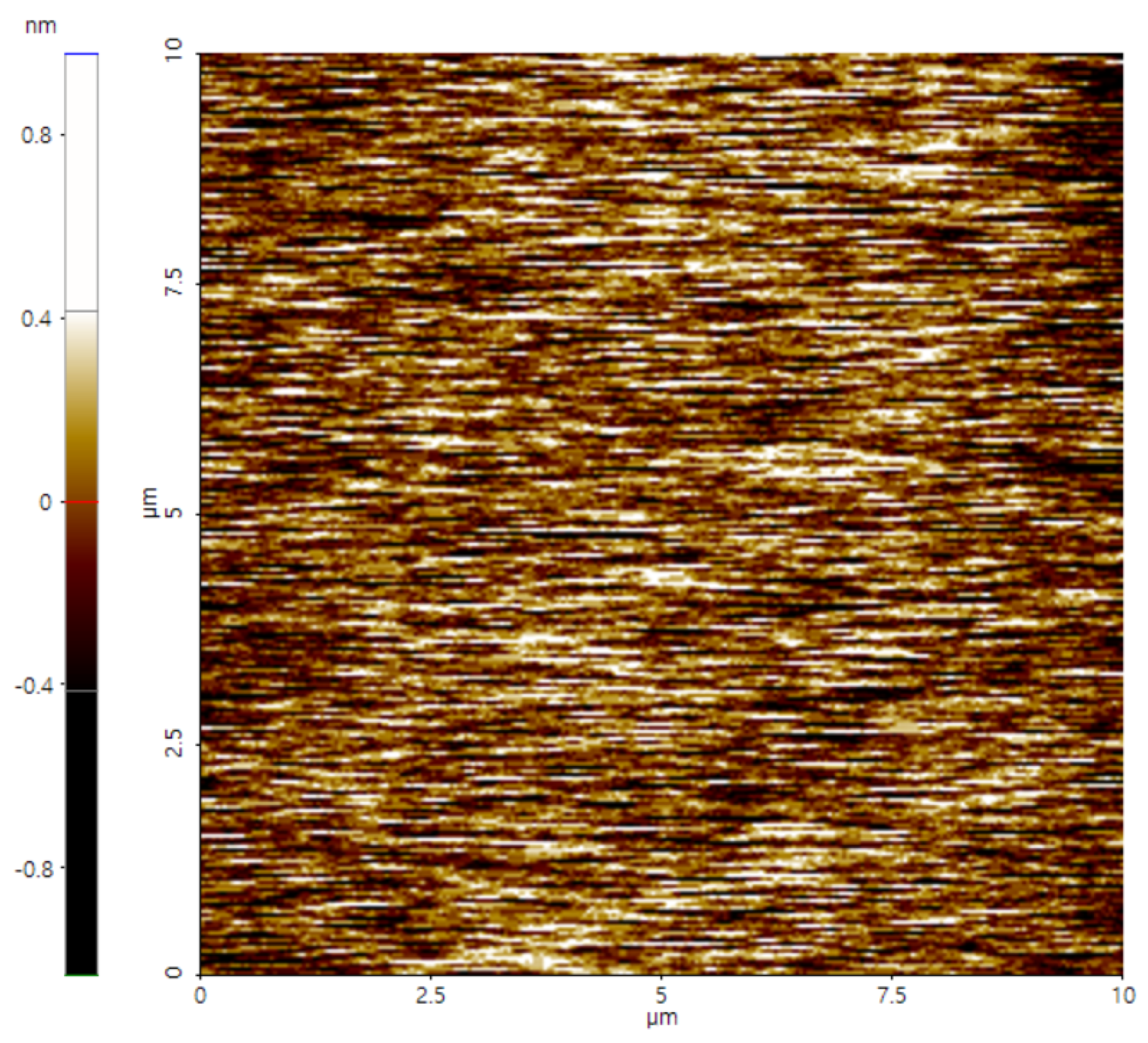
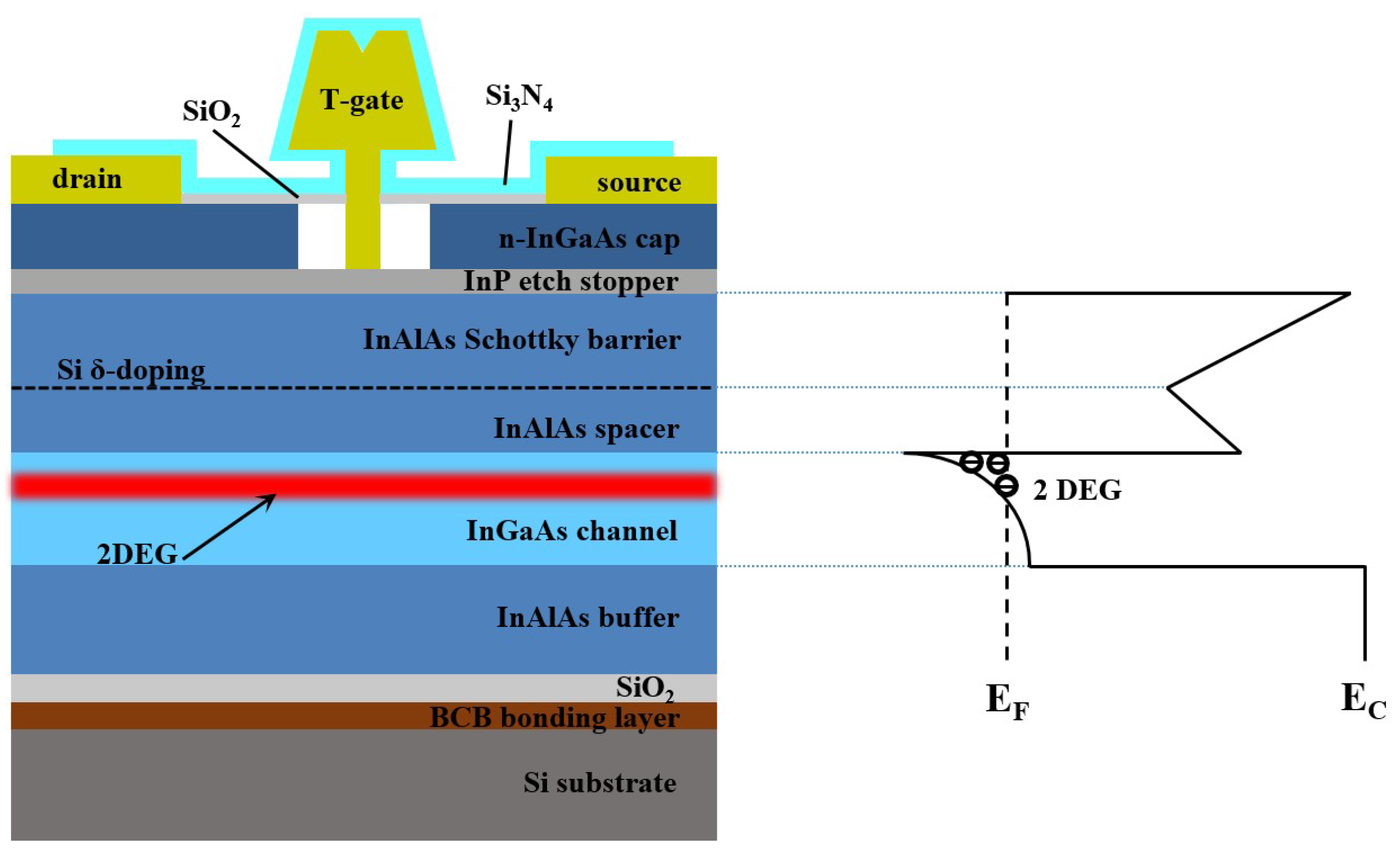
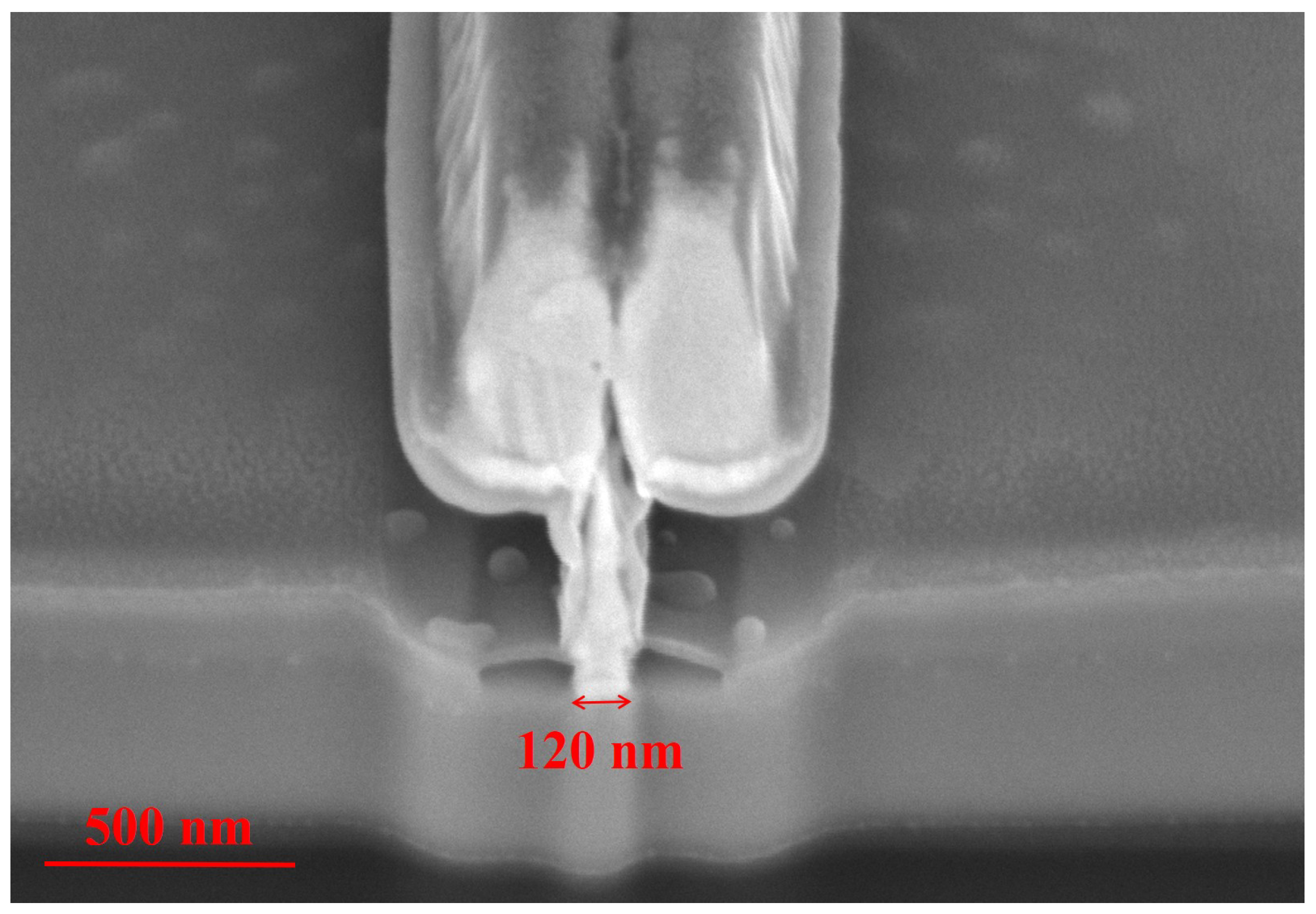
2. Experiment
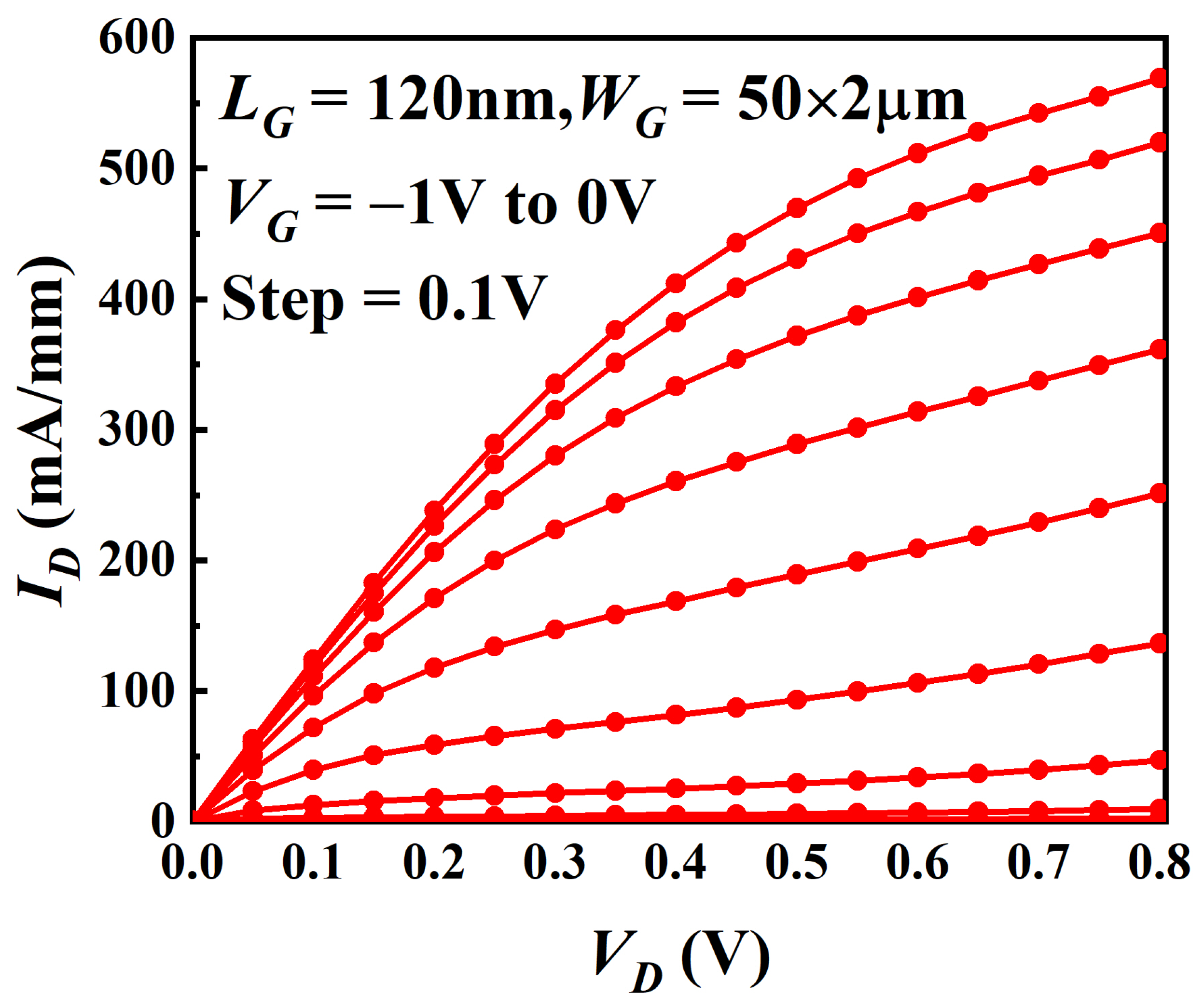
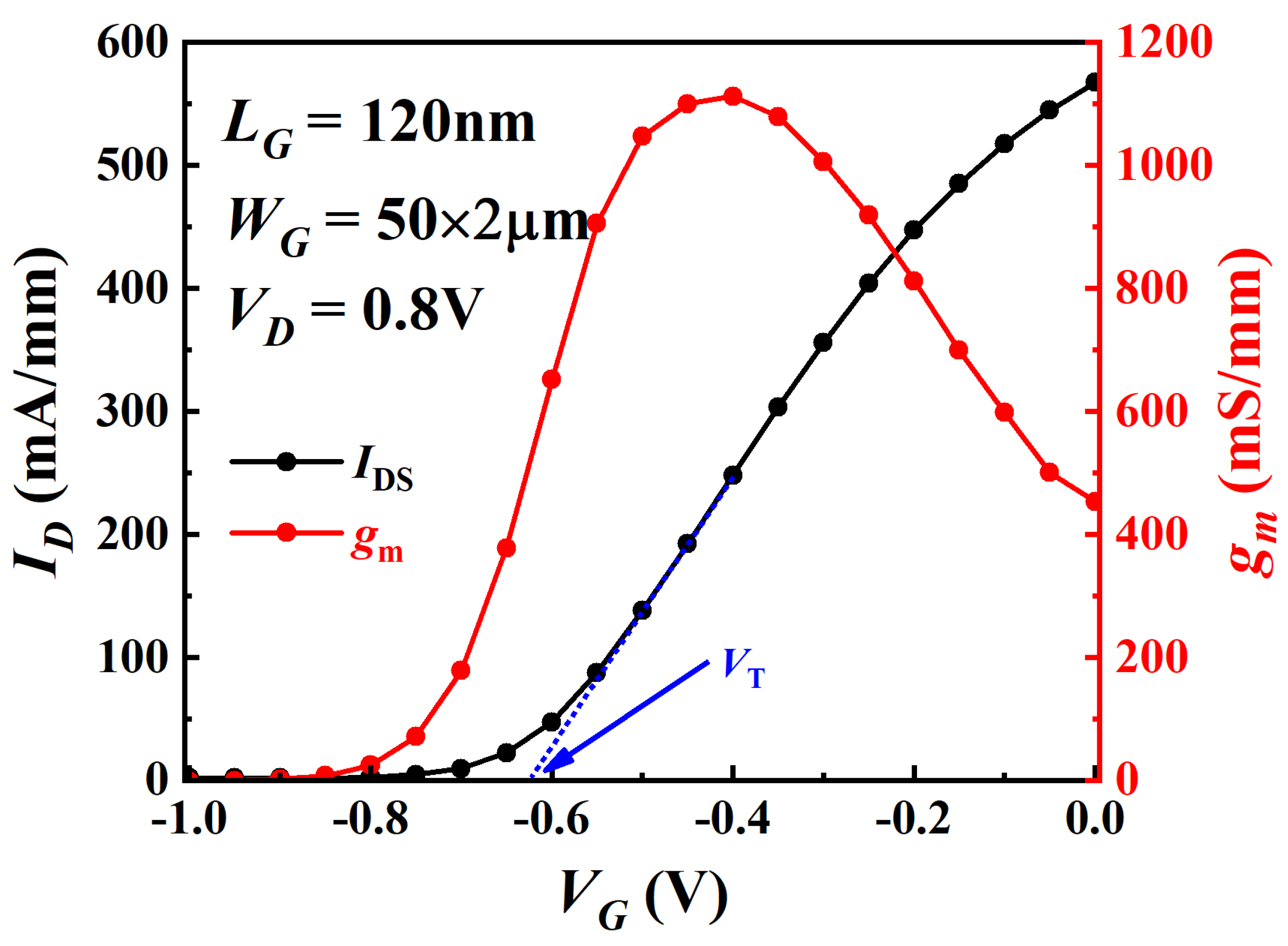
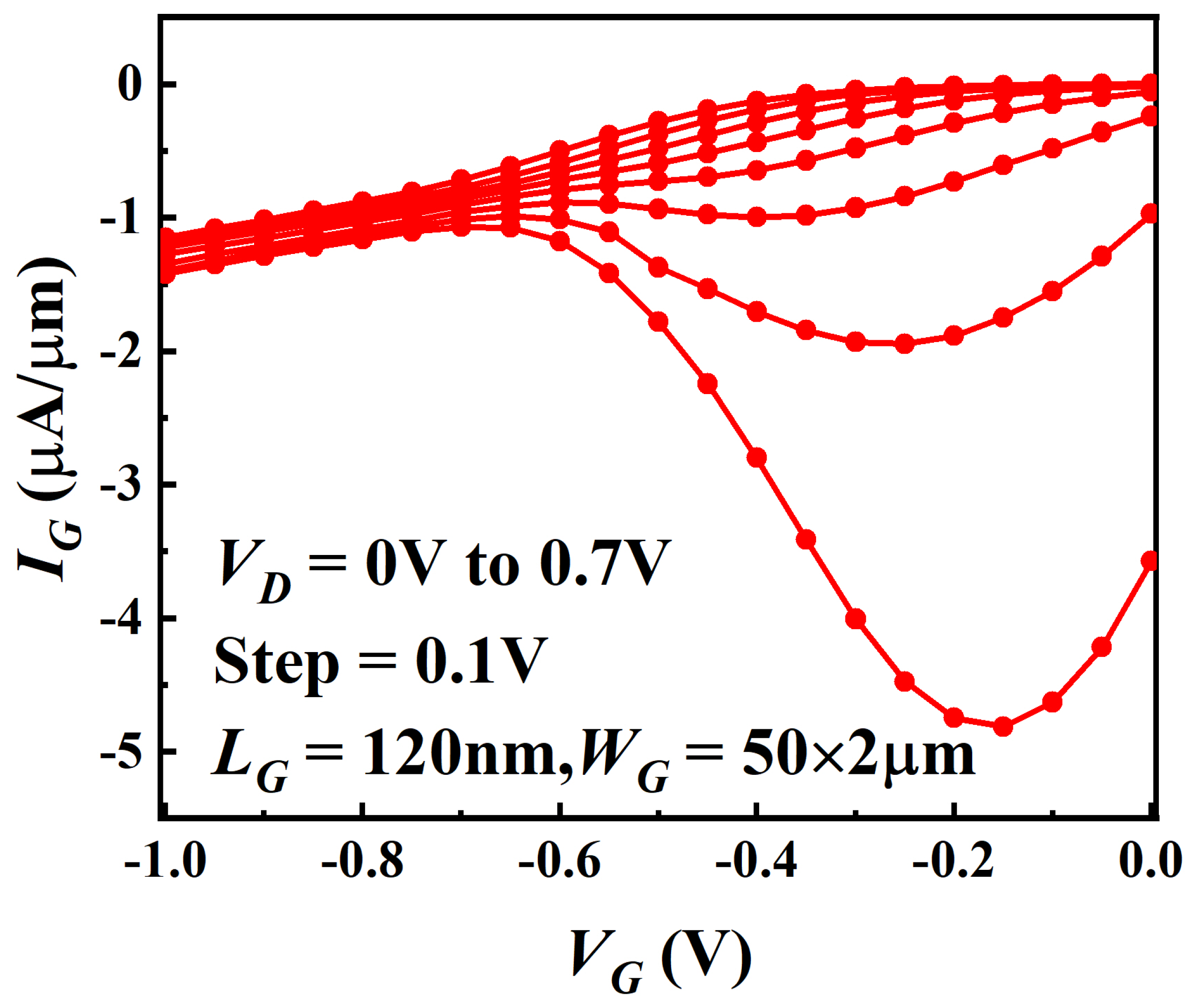
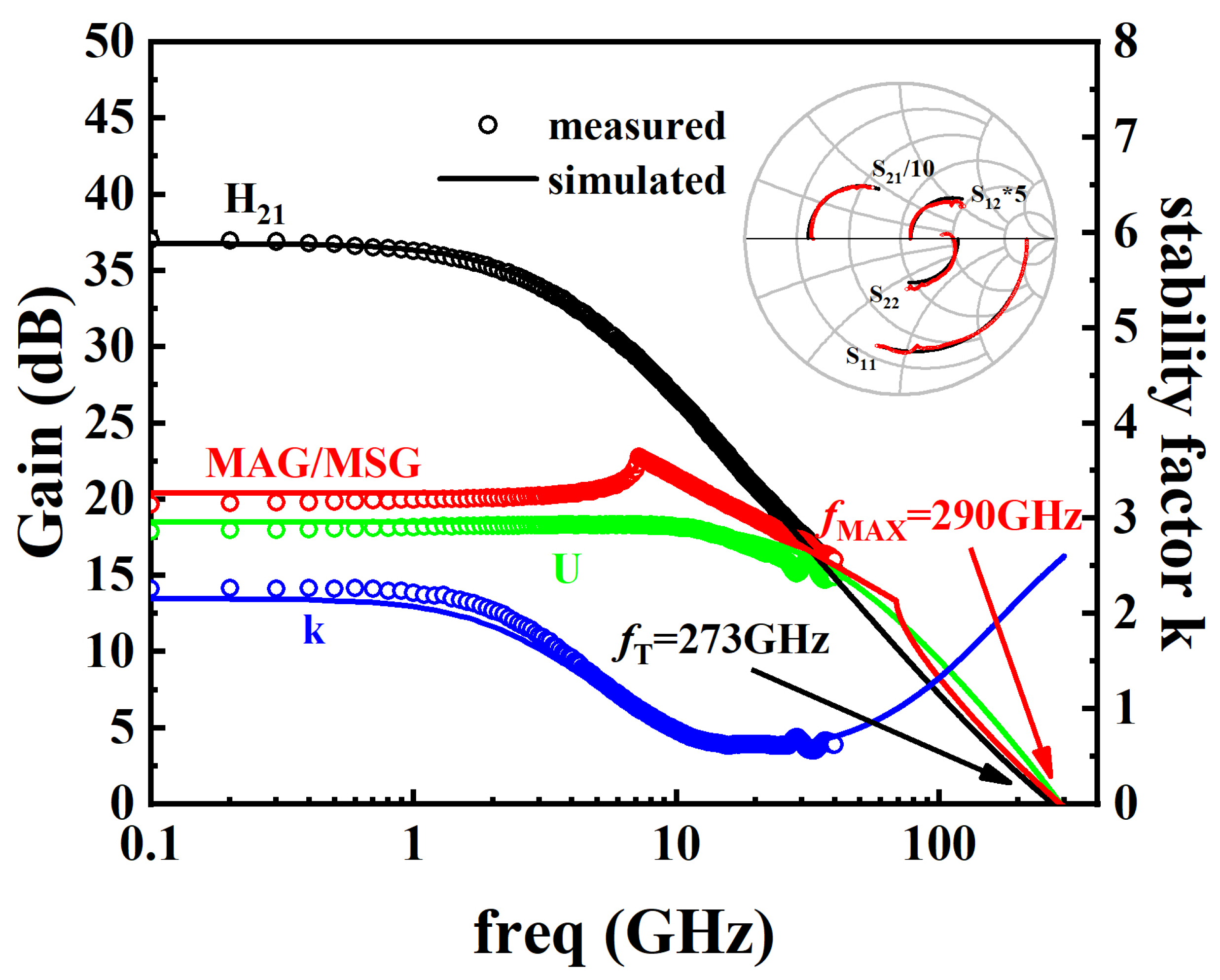
3. Result and Discussion
4. Conclusions
Author Contributions
Funding
Data Availability Statement
Conflicts of Interest
References
- Liu, Y.; Zhang, B.; Feng, Y.; Zhao, X.; Wang, J.; Ji, D.; Yang, Y.; Fan, Y. A G-band Balanced Power Amplifier based on InP HEMT Technology. In Proceedings of the 2020 IEEE MTT-S International Wireless Symposium (IWS), Shanghai, China, 20–23 September 2020; pp. 1–3. [Google Scholar] [CrossRef]
- Hamada, H.; Tsutsumi, T.; Matsuzaki, H.; Sugiyama, H.; Nosaka, H. 475-GHz 20-dB-Gain InP-HEMT Power Amplifier Using Neutralized Common-Source Architecture. In Proceedings of the 2020 IEEE/MTT-S International Microwave Symposium (IMS), Los Angeles, CA, USA, 4–6 August 2020; pp. 1121–1124. [Google Scholar] [CrossRef]
- Hamada, H.; Tsutsumi, T.; Itami, G.; Sugiyama, H.; Matsuzaki, H.; Okada, K.; Nosaka, H. 300-GHz 120-Gb/s Wireless Transceiver with High-Output-Power and High-Gain Power Amplifier Based on 80-nm InP-HEMT Technology. In Proceedings of the 2019 IEEE BiCMOS and Compound semiconductor Integrated Circuits and Technology Symposium (BCICTS), Nashville, TN, USA, 3–6 November 2019; pp. 1–4. [Google Scholar] [CrossRef]
- Mei, X.; Yoshida, W.; Lange, M.; Lee, J.; Zhou, J.; Liu, P.H.; Leong, K.; Zamora, A.; Padilla, J.; Sarkozy, S.; et al. First Demonstration of Amplification at 1 THz Using 25-nm InP High Electron Mobility Transistor Process. IEEE Electron. Device Lett. 2015, 36, 327–329. [Google Scholar] [CrossRef]
- Zhou, X.; Li, Q.; Tang, C.W.; Lau, K.M. 30nm enhancement-mode In0.53Ga0.47As MOSFETs on Si substrates grown by MOCVD exhibiting high transconductance and low on-resistance. In Proceedings of the 2012 International Electron Devices Meeting, San Francisco, CA, USA, 10–13 December 2012; pp. 32.5.1–32.5.4. [Google Scholar] [CrossRef]
- Waldron, N.; Wang, G.; Nguyen, N.D.; Orzali, T.; Merckling, C.; Brammertz, G.; Ong, P.; Winderickx, G.; Hellings, G.; Eneman, G.; et al. Integration of InGaAs Channel n-MOS Devices on 200mm Si Wafers Using the Aspect-Ratio-Trapping Technique. ECS Trans. 2012, 45, 115–128. [Google Scholar] [CrossRef] [Green Version]
- Jeong, J.; Kim, S.K.; Kim, J.; Geum, D.M.; Park, J.; Jang, J.H.; Kim, S. Stackable InGaAs-on-Insulator HEMTs for Monolithic 3-D Integration. IEEE Trans. Electron Devices 2021, 68, 2205–2211. [Google Scholar] [CrossRef]
- Tessmann, A.; Leuther, A.; Heinz, F.; Bernhardt, F.; John, L.; Massler, H.; Czornomaz, L.; Merkle, T. 20-nm In0.8Ga0.2As MOSHEMT MMIC Technology on Silicon. IEEE J. Solid-State Circuits 2019, 54, 2411–2418. [Google Scholar] [CrossRef]
- Zota, C.B.; Convertino, C.; Baumgartner, Y.; Sousa, M.; Caimi, D.; Czornomaz, L. High Performance Quantum Well InGaAs-On-Si MOSFETs With sub-20 nm Gate Length For RF Applications. In Proceedings of the 2018 IEEE International Electron Devices Meeting (IEDM), San Francisco, CA, USA, 1–5 December 2018; pp. 39.4.1–39.4.4. [Google Scholar] [CrossRef]
- Vandooren, A.; Franco, J.; Parvais, B.; Wu, Z.; Witters, L.; Walke, A.; Li, W.; Peng, L.; Desphande, V.; Bufler, F.M.; et al. 3D sequential stacked planar devices on 300 mm wafers featuring replacement metal gate junction-less top devices processed at 525 °C with improved reliability. In Proceedings of the 2018 IEEE Symposium on VLSI Technology, Honolulu, HI, USA, 18–22 June 2018; pp. 69–70. [Google Scholar] [CrossRef]
- Lee, S.; Kim, S.K.; Han, J.; Song, J.D.; Jun, D.; Kim, S. Epitaxial Lift-Off Technology for Large Size III–V-on-Insulator Substrate. IEEE Electron. Device Lett. 2019, 40, 1732–1735. [Google Scholar] [CrossRef]
- Kim, S.K.; Shim, J.; Geum, D.; Kim, J.; Kim, C.Z.; Kim, H.; Song, J.D.; Choi, S.; Kim, D.H.; Choi, W.J.; et al. Impact of Ground Plane Doping and Bottom-Gate Biasing on Electrical Properties in In0.53Ga0.47As-OI MOSFETs and Donor Wafer Reusability Toward Monolithic 3-D Integration With In0.53Ga0.47As Channel. IEEE Trans. Electron. Devices 2018, 65, 1862–1868. [Google Scholar] [CrossRef]
- Convertino, C.; Zota, C.; Sant, S.; Eltes, F.; Sousa, M.; Caimi, D.; Schenk, A.; Czornomaz, L. InGaAs-on-Insulator FinFETs with Reduced Off-Current and Record Performance. In Proceedings of the 2018 IEEE International Electron Devices Meeting (IEDM), San Francisco, CA, USA, 1–5 December 2018; pp. 39.2.1–39.2.4. [Google Scholar] [CrossRef]
- Takagi, S.; Ahn, D.H.; Gotow, T.; Noguchi, M.; Nishi, K.; Kim, S.; Yokoyama, M.; Chang, C.; Yoon, S.; Yokoyama, C.; et al. III–V-based low power CMOS devices on Si platform. In Proceedings of the 2017 IEEE International Conference on IC Design and Technology (ICICDT), Austin, TX, USA, 23–25 May 2017; pp. 1–4. [Google Scholar] [CrossRef]
- Yadav, S.; Kumar, A.; Nguyen, X.S.; Lee, K.H.; Liu, Z.; Xing, W.; Masudy-Panah, S.; Lee, K.; Tan, C.S.; Fitzgerald, E.A.; et al. High mobility In0.30Ga0.70As MOSHEMTs on low threading dislocation density 200 mm Si substrates: A technology enabler towards heterogeneous integration of low noise and medium power amplifiers with Si CMOS. In Proceedings of the 2017 IEEE International Electron Devices Meeting (IEDM), San Francisco, CA, USA, 2–6 December 2017; pp. 17.4.1–17.4.4. [Google Scholar] [CrossRef]
- Nguyen, X.S.; Yadav, S.; Lee, K.H.; Kohen, D.; Kumar, A.; Made, R.I.; Lee, K.E.K.; Chua, S.J.; Gong, X.; Fitzgerald, E.A. MOCVD Growth of High Quality InGaAs HEMT Layers on Large Scale Si Wafers for Heterogeneous Integration With Si CMOS. IEEE Trans. Semicond. Manuf. 2017, 30, 456–461. [Google Scholar] [CrossRef]
- Reuter, R.; Agethen, M.; Auer, U.; Waasen, S.v.; Peters, D.; Brockerhoff, W.; Tegude, F.J. Investigation and modeling of impact ionization with regard to the RF and noise behavior of HFET. IEEE Trans. Microw. Theory Tech. 1997, 45, 977–983. [Google Scholar] [CrossRef]
- Ruiz, D.C.; Saranovac, T.; Han, D.; Ostinelli, O.; Bolognesi, C.R. Impact Ionization Control in 50 nm Low-Noise High-Speed InP HEMTs with InAs Channel Insets. In Proceedings of the 2019 IEEE International Electron Devices Meeting (IEDM), San Francisco, CA, USA, 7–11 December 2019; pp. 9.3.1–9.3.4. [Google Scholar] [CrossRef]
- del Alamo, J.A. Nanometre-scale electronics with III–V compound semiconductors. Nature 2011, 479, 317–323. [Google Scholar] [CrossRef] [PubMed]
- Chang, E.Y.; Huang, J.C.; Lin, Y.C.; Hsieh, Y.C.; Chang, C.Y. AlGaAs/InGaAs High Electron Mobility Transistor Grown on Si Substrate with Ge/GexSi1-xMetamorphic Buffer Layers. Jpn. J. Appl. Phys. 2008, 47, 7069–7072. [Google Scholar] [CrossRef]
- Bollaert, S.; Wallaert, X.; Lepilliet, S.; Cappy, A.; Jalaguier, E.; Pocas, S.; Aspar, B. 0.12 µm transferred-substrate In0.52Al0.48As/In0.53Ga0.47As HEMTs on silicon wafer. IEEE Electron. Device Lett. 2002, 23, 73–75. [Google Scholar] [CrossRef]


| (fF) | (fF) | (fF) | (mS) | () | () | () | () | g (mS) | Tau (fs) |
|---|---|---|---|---|---|---|---|---|---|
| 62.1 | 9.5 | 11.5 | 10 | 1.6 | 4.5 | 3 | 7.5 | 116 | 400 |
Publisher’s Note: MDPI stays neutral with regard to jurisdictional claims in published maps and institutional affiliations. |
© 2022 by the authors. Licensee MDPI, Basel, Switzerland. This article is an open access article distributed under the terms and conditions of the Creative Commons Attribution (CC BY) license (https://creativecommons.org/licenses/by/4.0/).
Share and Cite
Wang, B.; Wang, Y.; Feng, R.; Wei, H.; Cao, S.; Liu, T.; Liu, X.; Li, H.; Ding, P.; Jin, Z. High-Performance InGaAs HEMTs on Si Substrates for RF Applications. Electronics 2022, 11, 259. https://doi.org/10.3390/electronics11020259
Wang B, Wang Y, Feng R, Wei H, Cao S, Liu T, Liu X, Li H, Ding P, Jin Z. High-Performance InGaAs HEMTs on Si Substrates for RF Applications. Electronics. 2022; 11(2):259. https://doi.org/10.3390/electronics11020259
Chicago/Turabian StyleWang, Bo, Yanfu Wang, Ruize Feng, Haomiao Wei, Shurui Cao, Tong Liu, Xiaoyu Liu, Haiou Li, Peng Ding, and Zhi Jin. 2022. "High-Performance InGaAs HEMTs on Si Substrates for RF Applications" Electronics 11, no. 2: 259. https://doi.org/10.3390/electronics11020259
APA StyleWang, B., Wang, Y., Feng, R., Wei, H., Cao, S., Liu, T., Liu, X., Li, H., Ding, P., & Jin, Z. (2022). High-Performance InGaAs HEMTs on Si Substrates for RF Applications. Electronics, 11(2), 259. https://doi.org/10.3390/electronics11020259