A Novel Radiation-Hardened CCDM-TSPC Compared with Seven Well-Known RHBD Flip-Flops in 180 nm CMOS Process

Abstract
:1. Introduction
- Circuit level: Radiation-hardened-by-design (RHBD) technology is the circuit-level approach. Because it may enhance the radiation immunity of chips and offer significant design freedom without depending on external conditions, RHBD technology is frequently used in the high-reliability design of circuits [14,15,16,17].
- A relatively thorough review and classification of existing D flip-flops for radiation immunity is produced, so as to better support future radiation immunity research in sequential logic circuits.
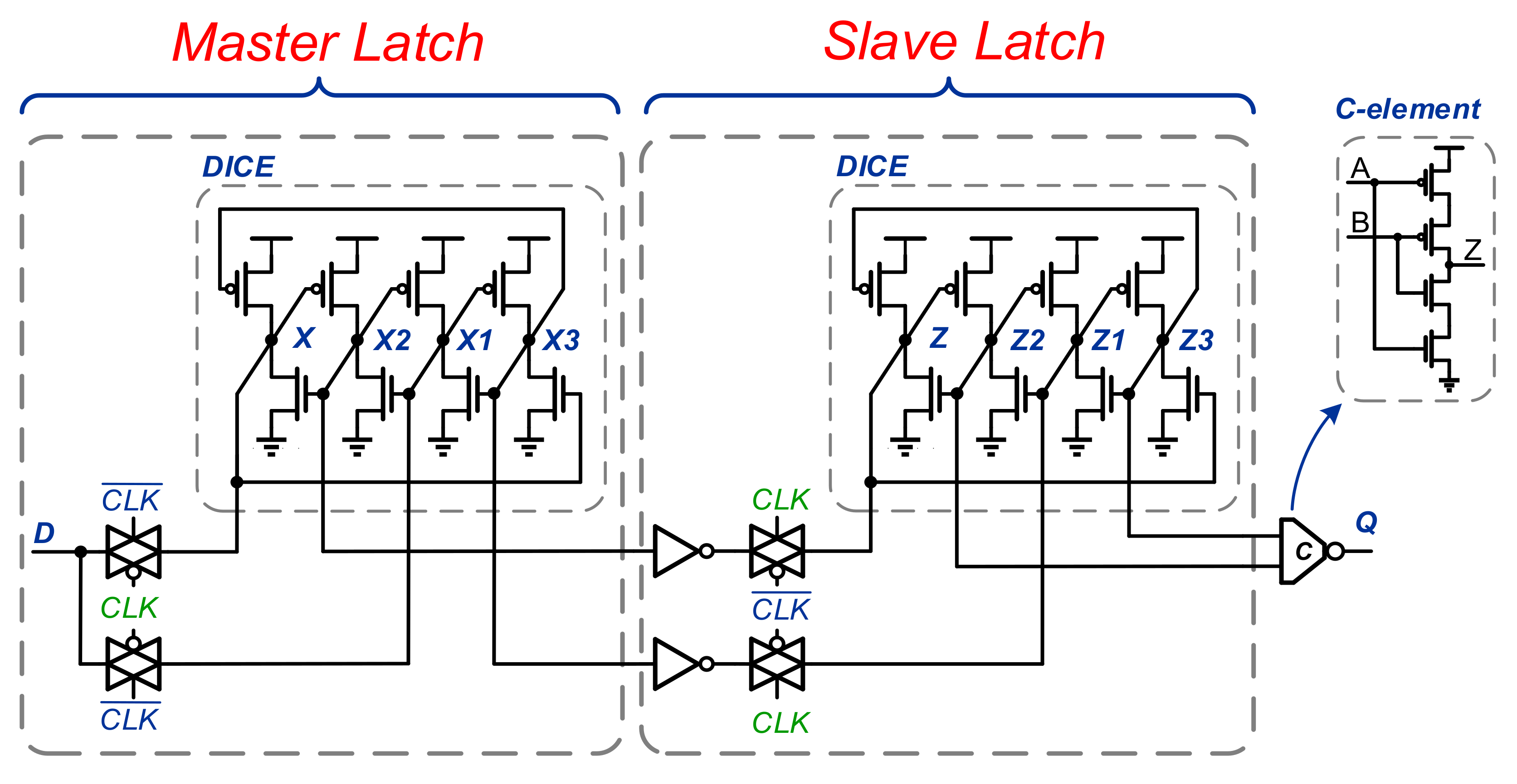
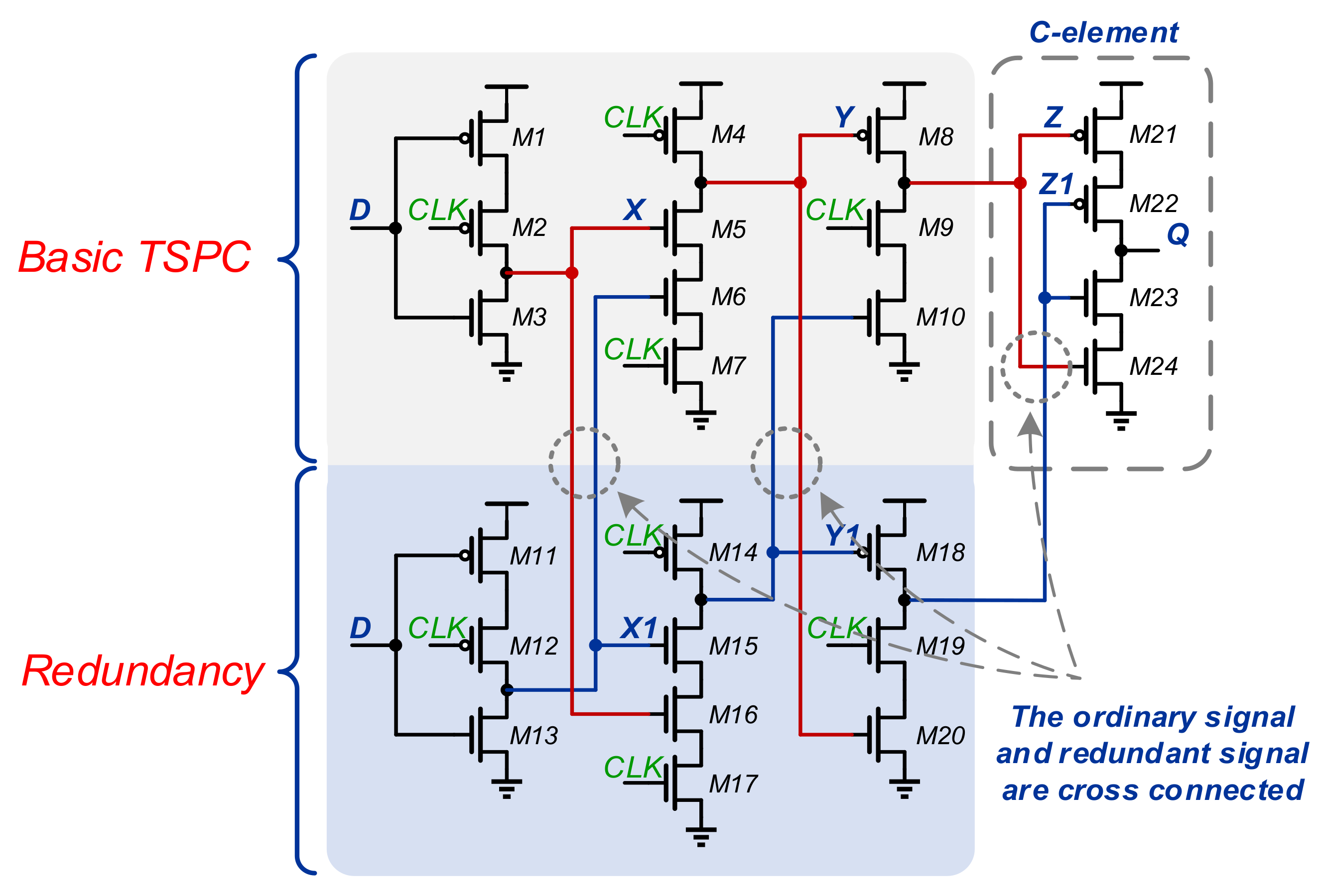
- A novel cross-connected dual modular redundant TSPC D flip-flop (CCDM-TSPC) is proposed. Because every vulnerable area of the circuit is shielded by using means of cross-connection, CCDM-TSPC is totally immune to SEUs.
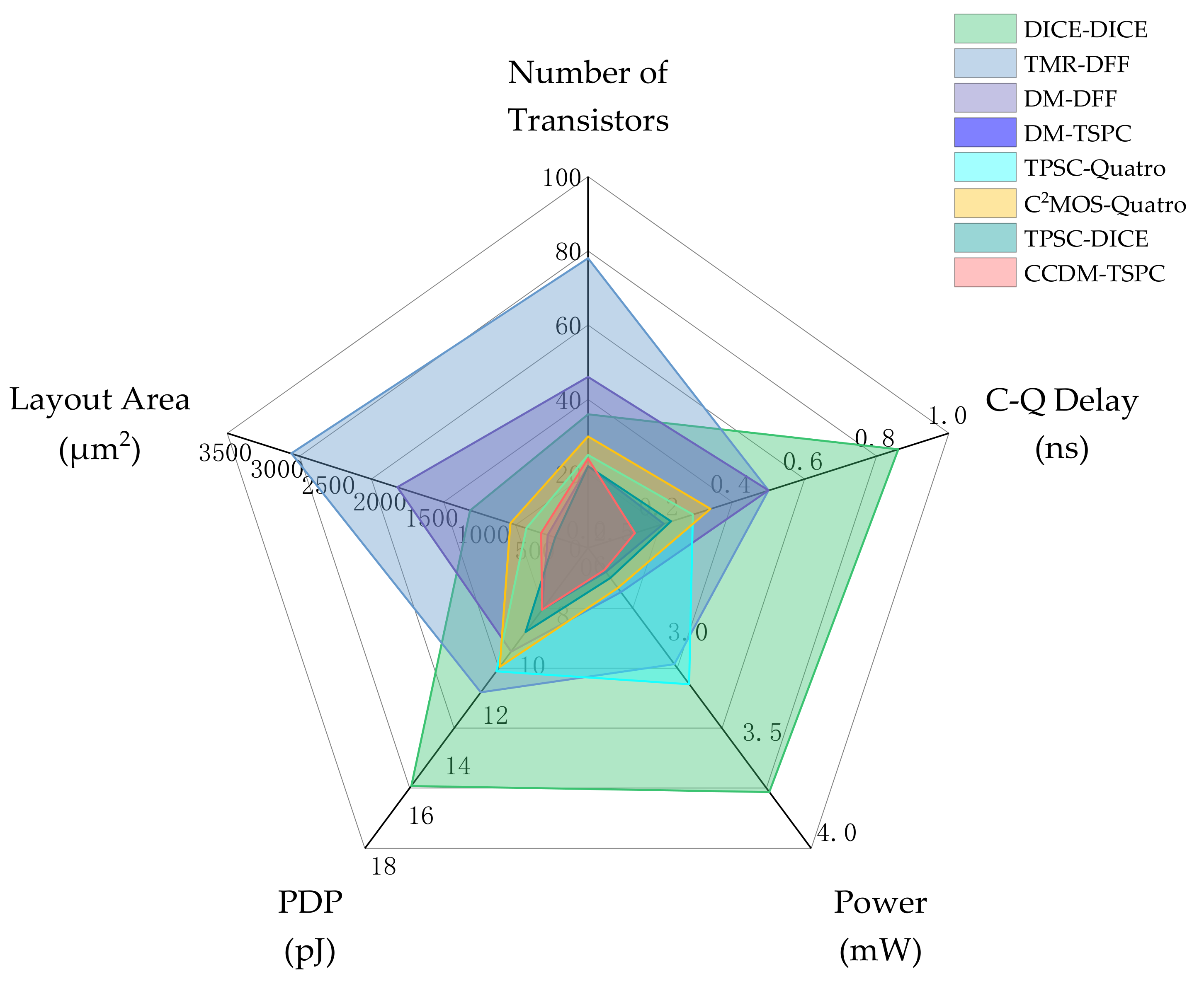
- The C-Q delay, power consumption, and power delay product (PDP) of CCDM-TSPC are the smallest compared with seven mentioned traditional structures. In comparison with the conventional TMR and DMR structure, the layout area of CCDM-TSPC has been decreased by more than 75%.
2. Existing Soft Error Robust Flip-Flop Designs
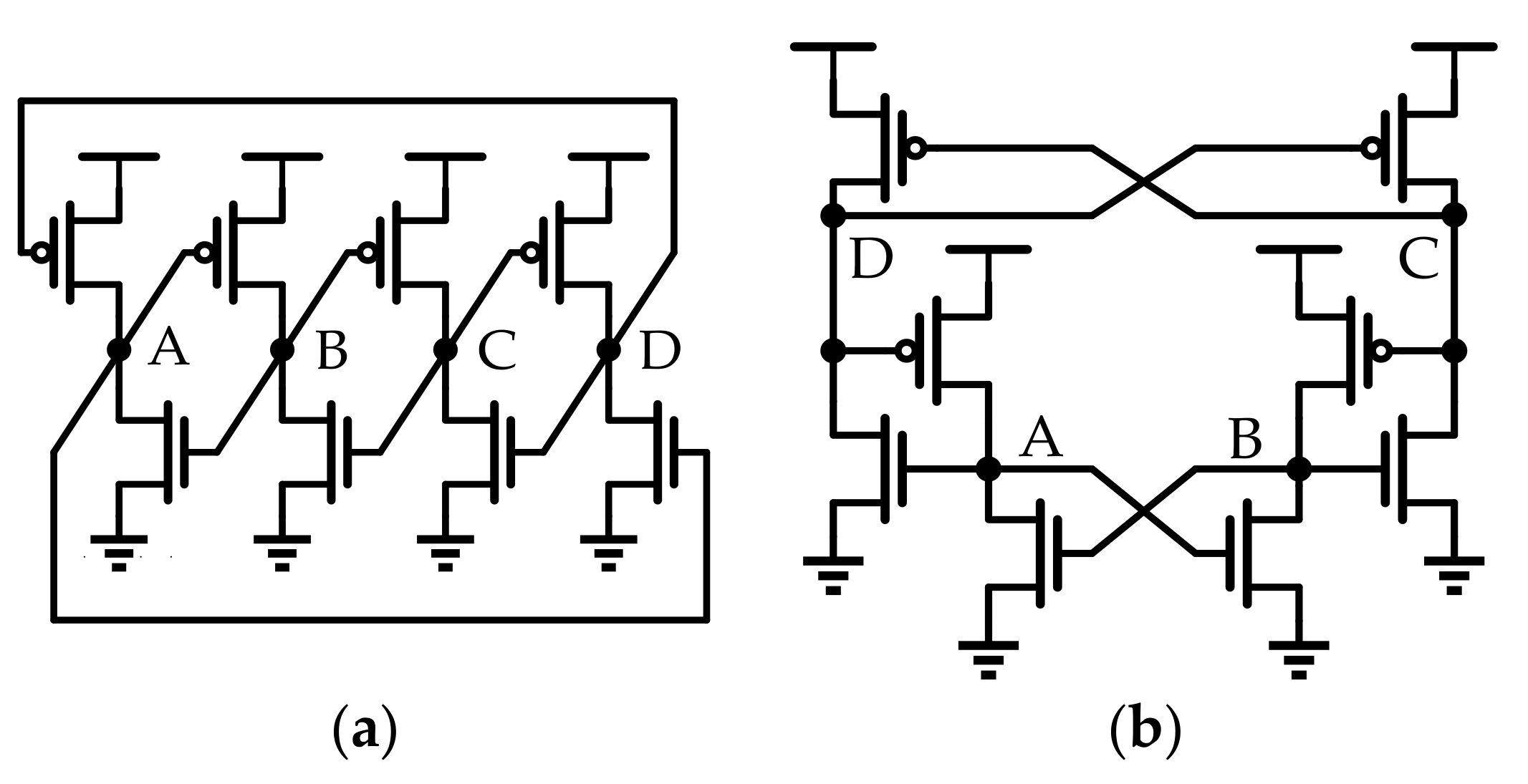
2.1. DICE-DICE
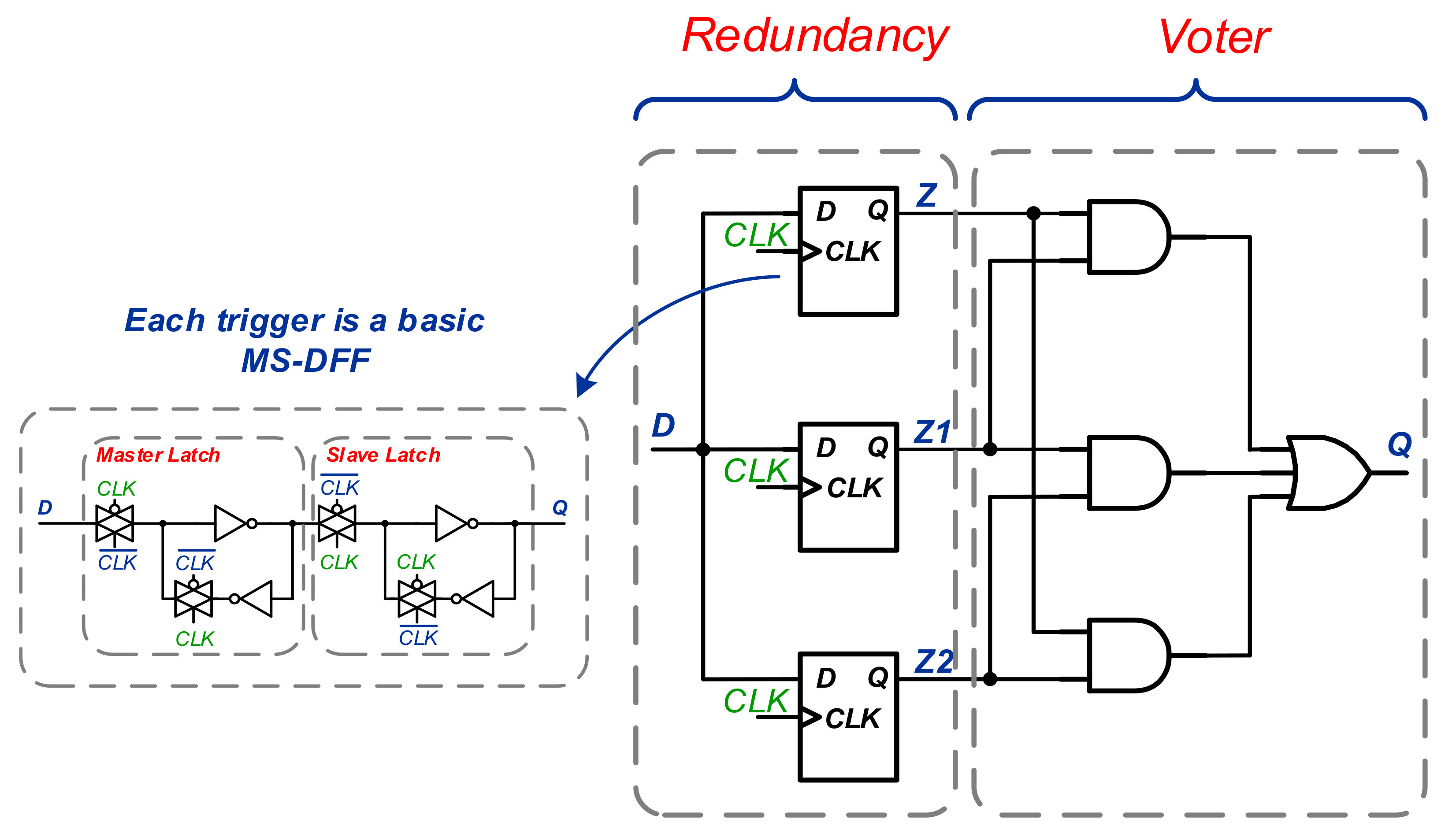
2.2. TMR-DFF
2.3. DM-DFF
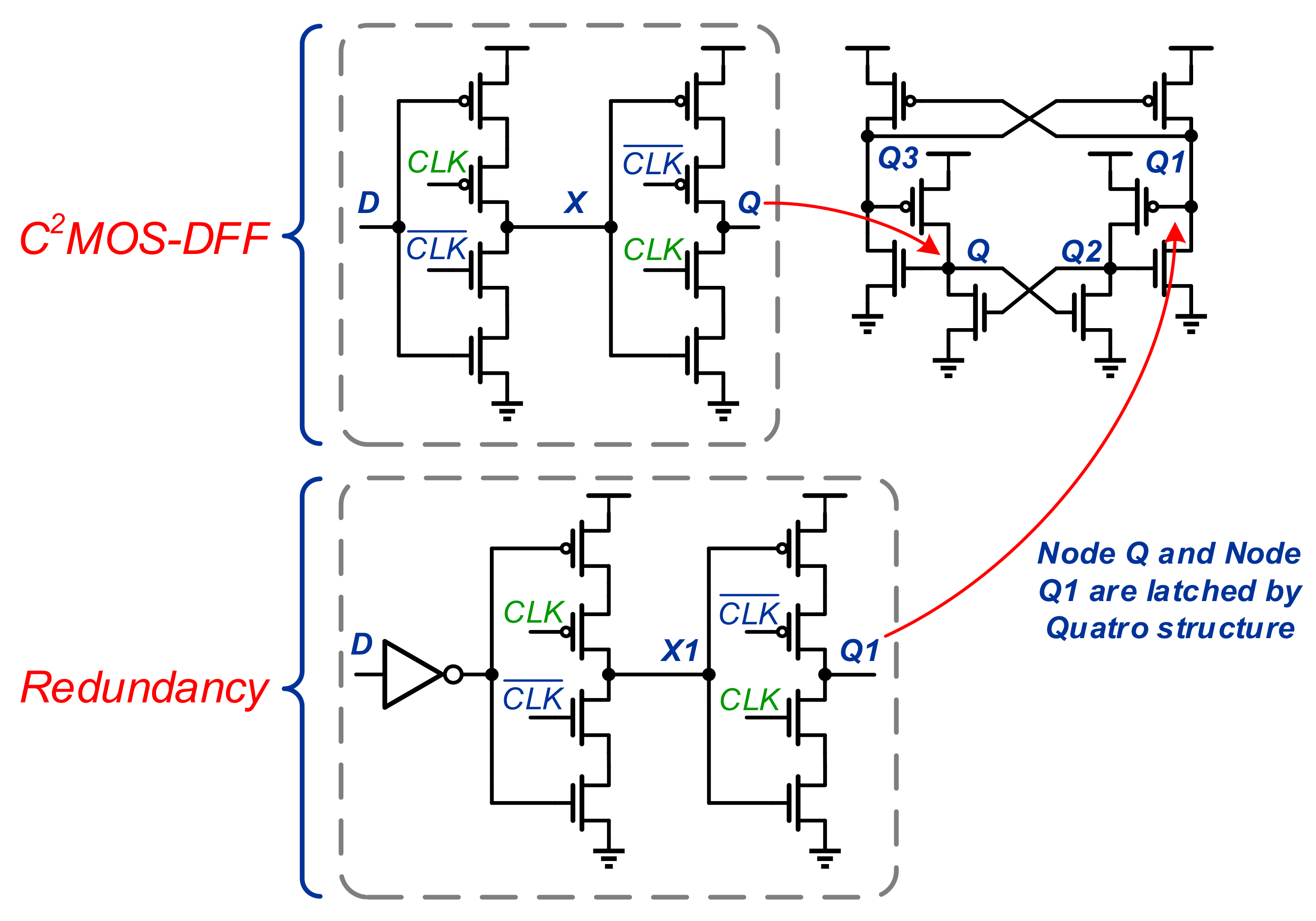
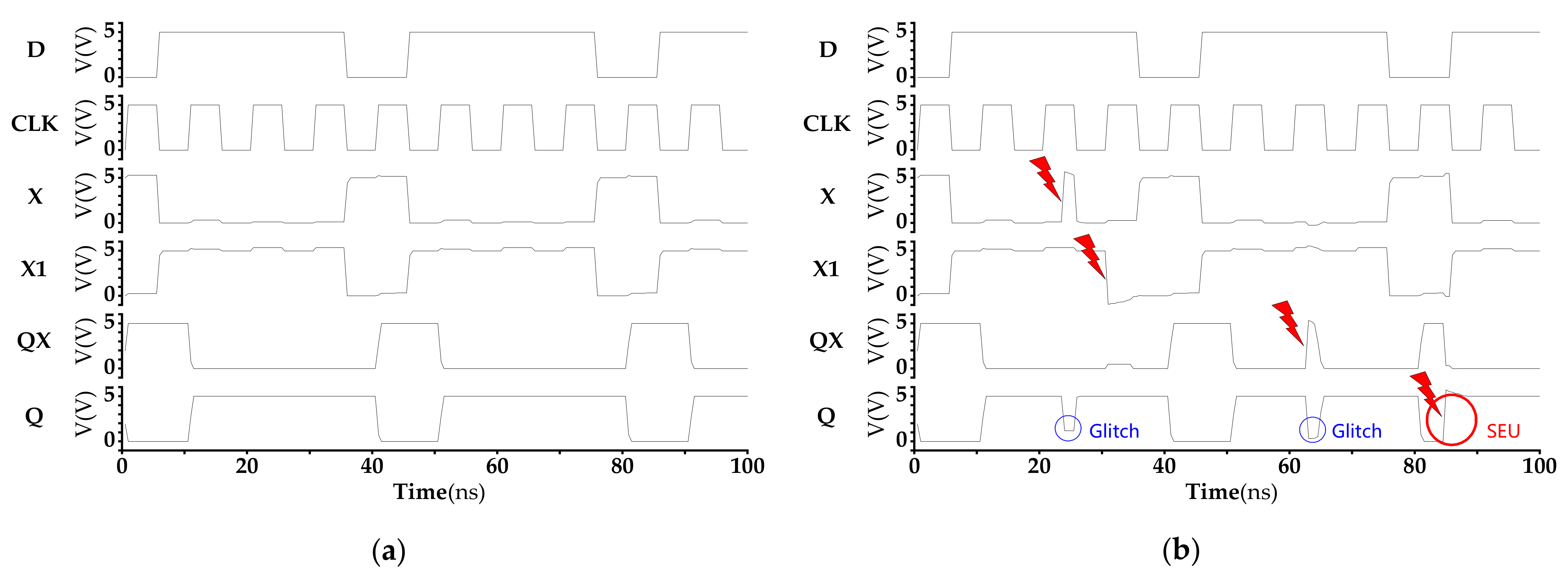
2.4. DM-TSPC
2.5. TSPC-Quatro
2.6. C2MOS-Quatro
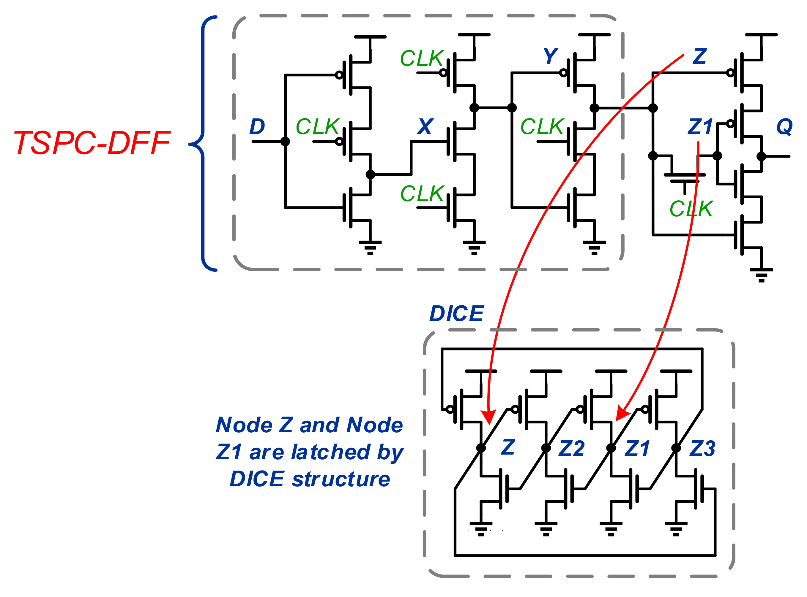
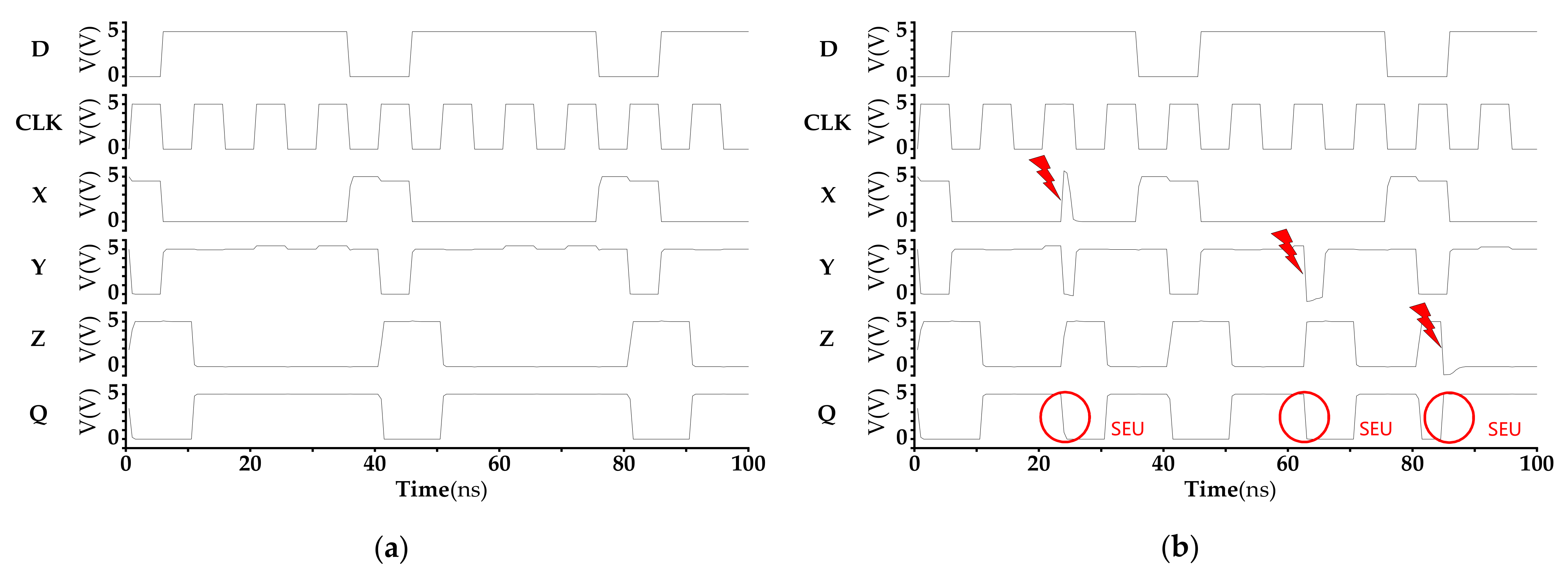
2.7. TSPC-DICE
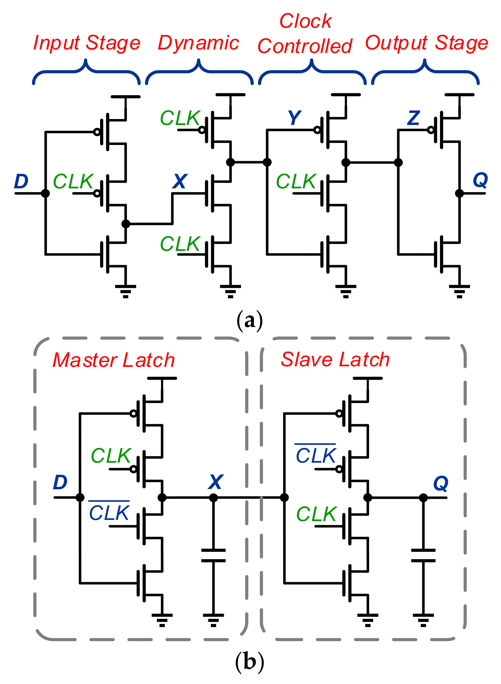
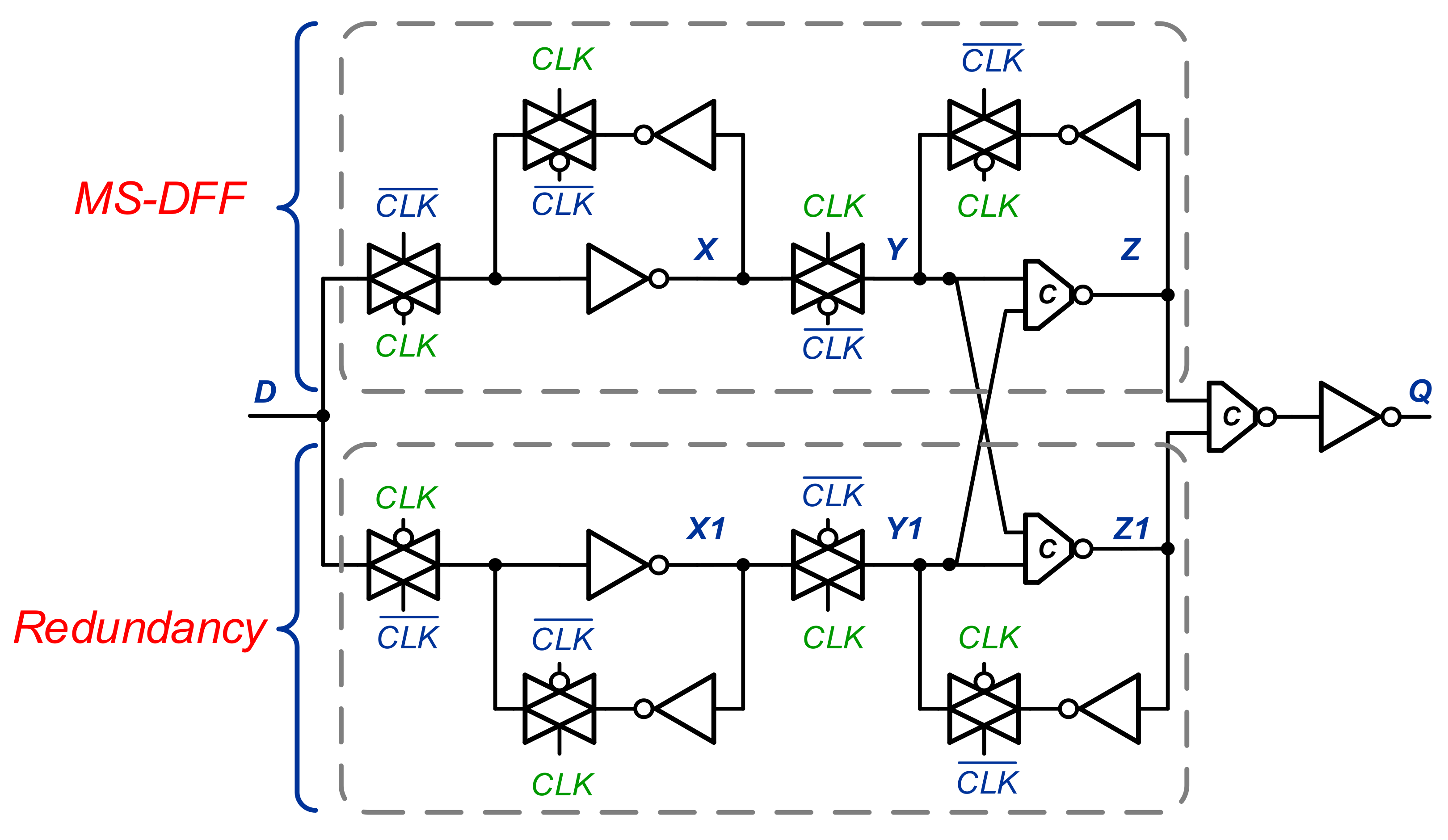
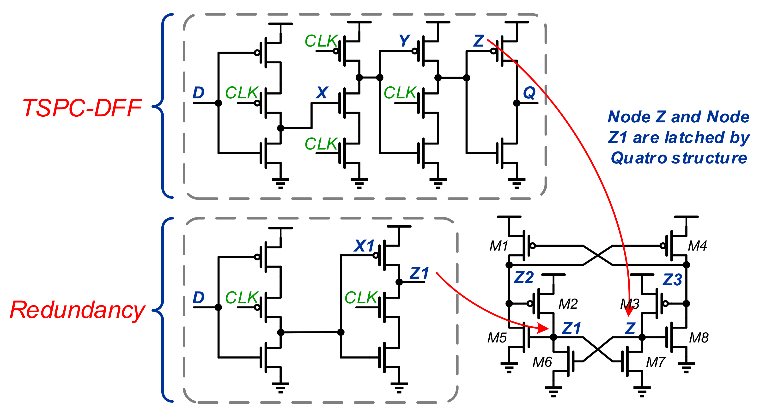
3. Proposed Soft Error Robust Flip-Flop Designs
3.1. Working
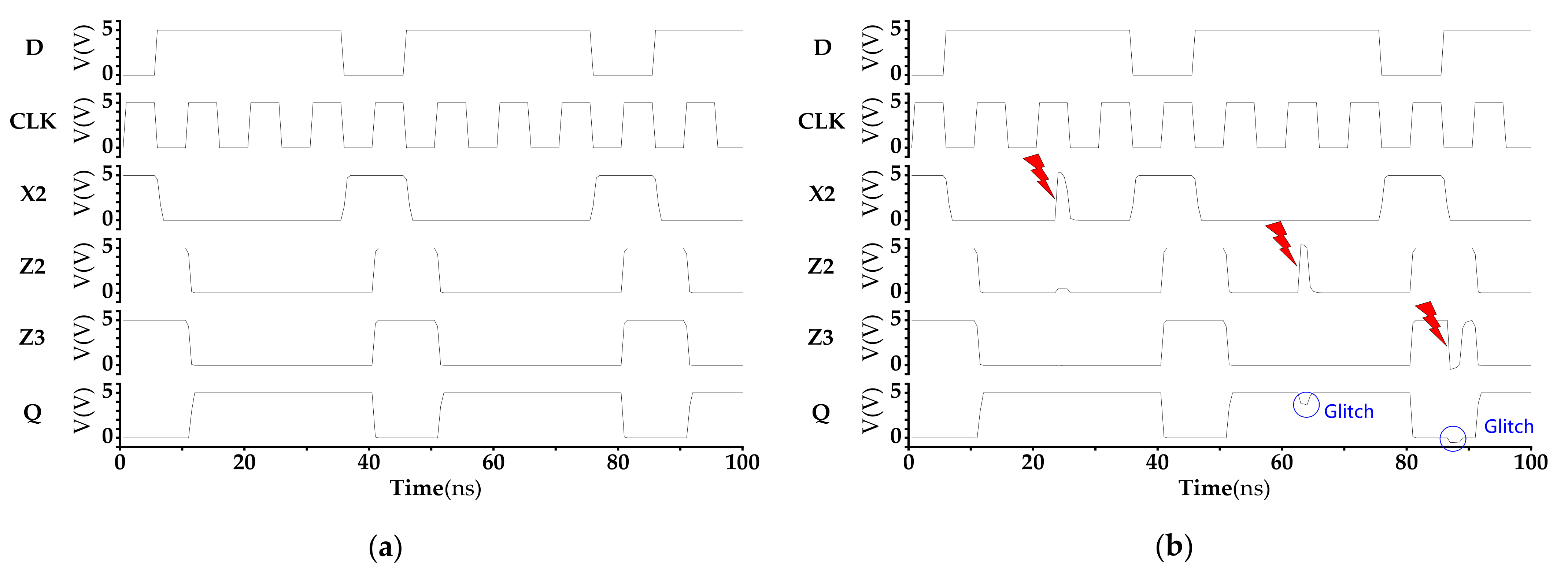
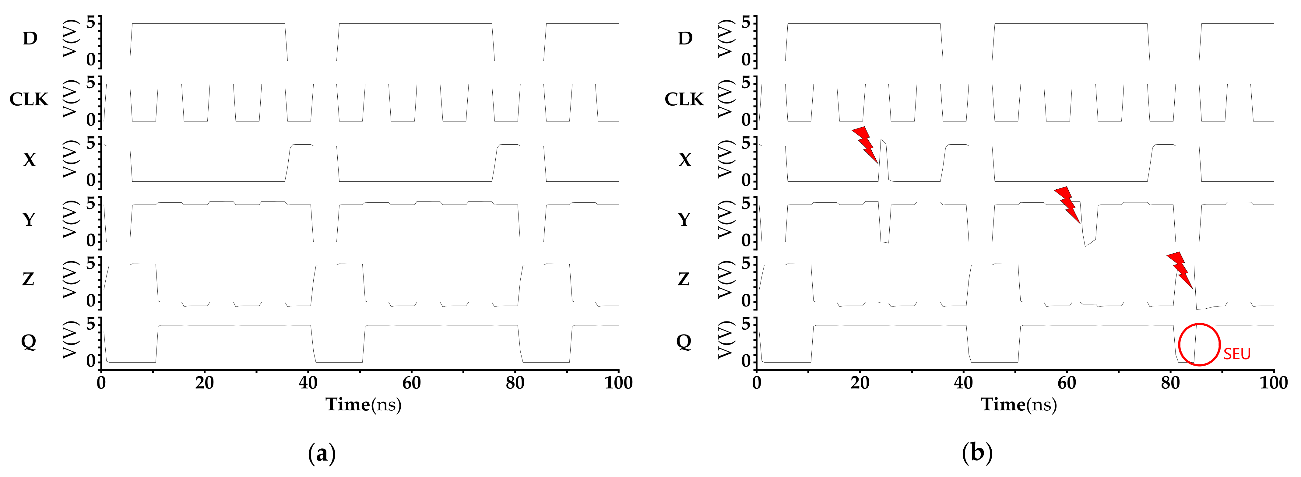
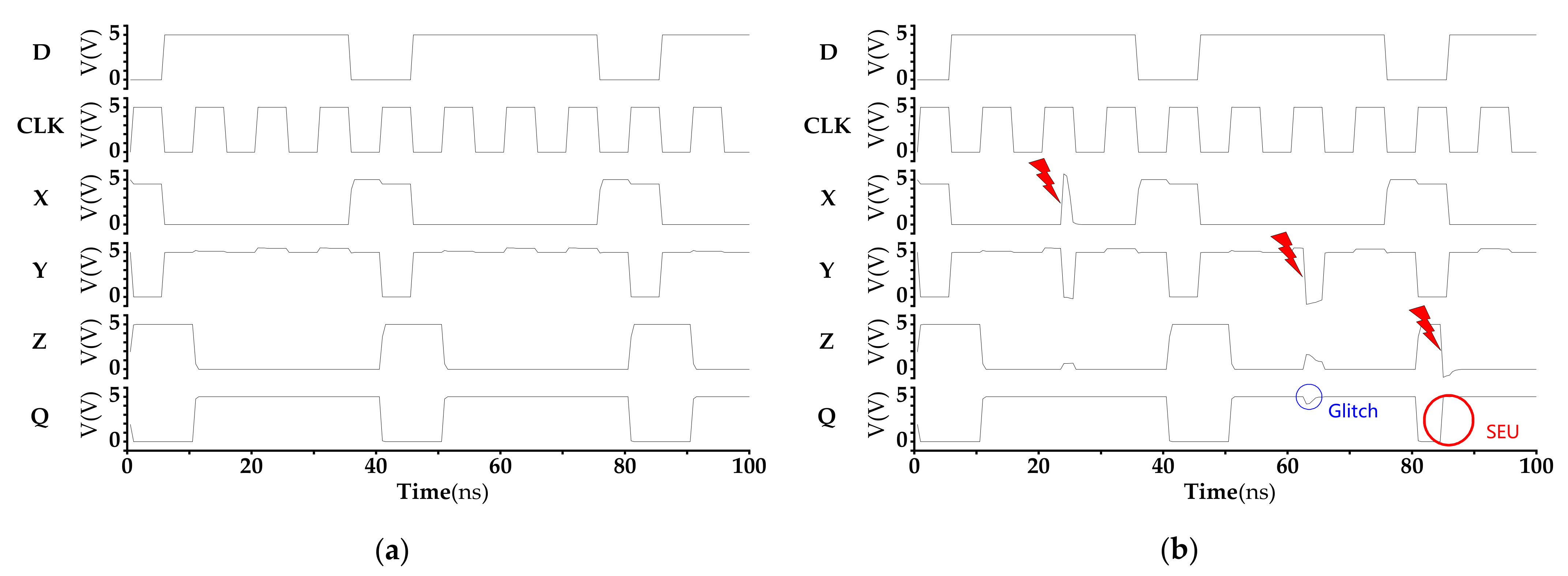
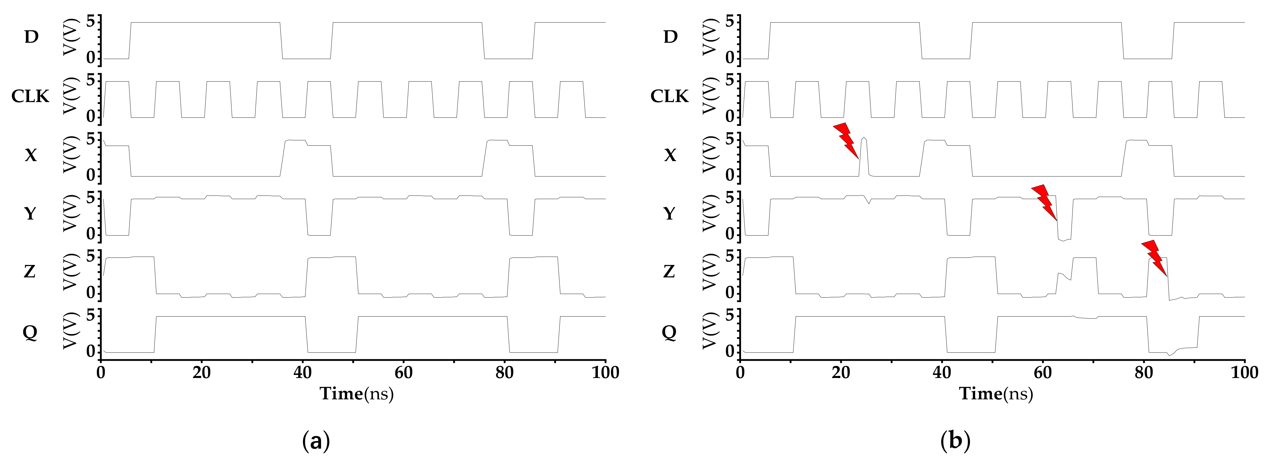
3.2. Soft Error Analysis
4. Performance Evaluation and Analysis
4.1. Design Complexity
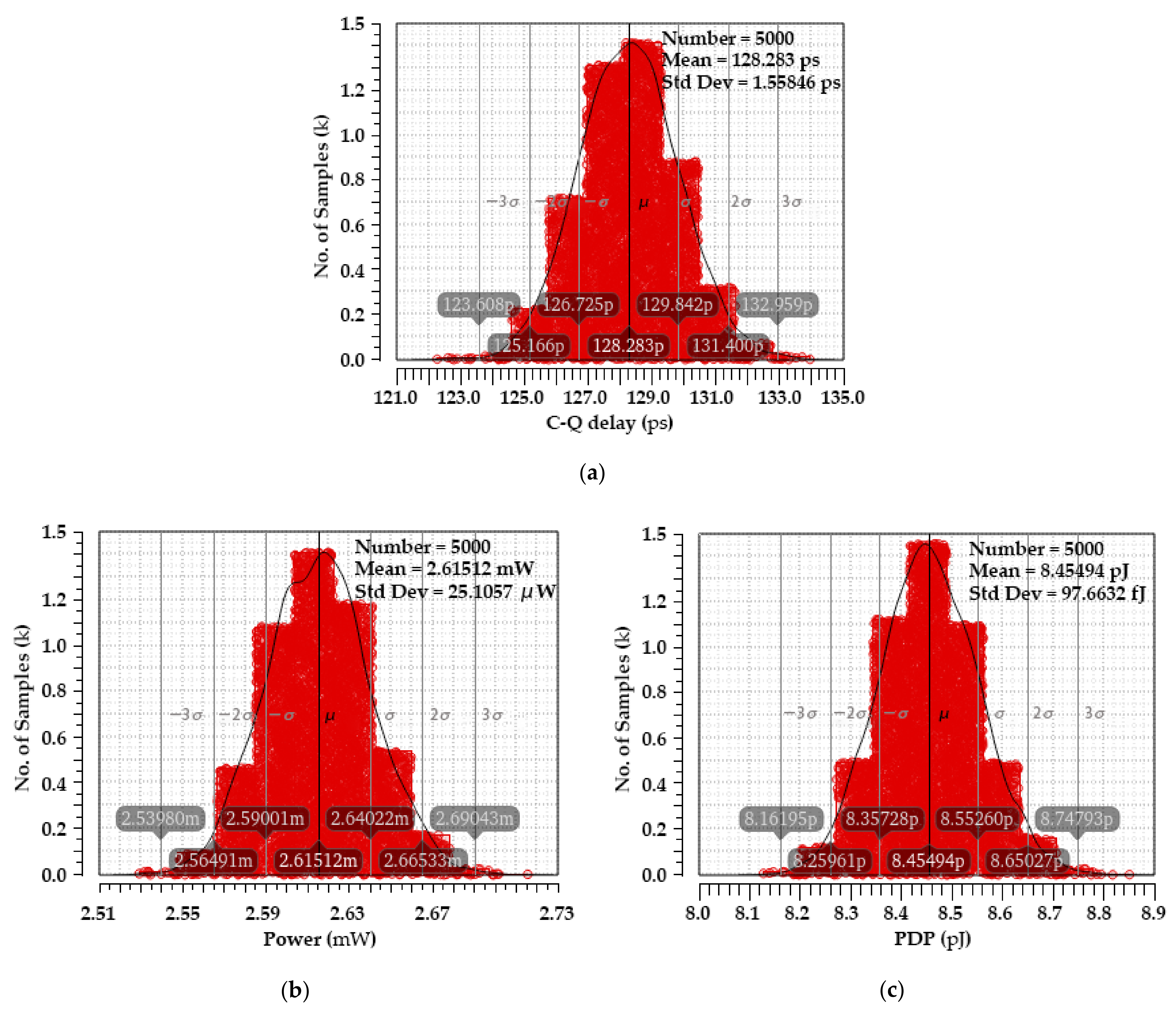
4.2. C-Q Delay
4.3. Power Consumption
4.4. Power Delay Product (PDP)
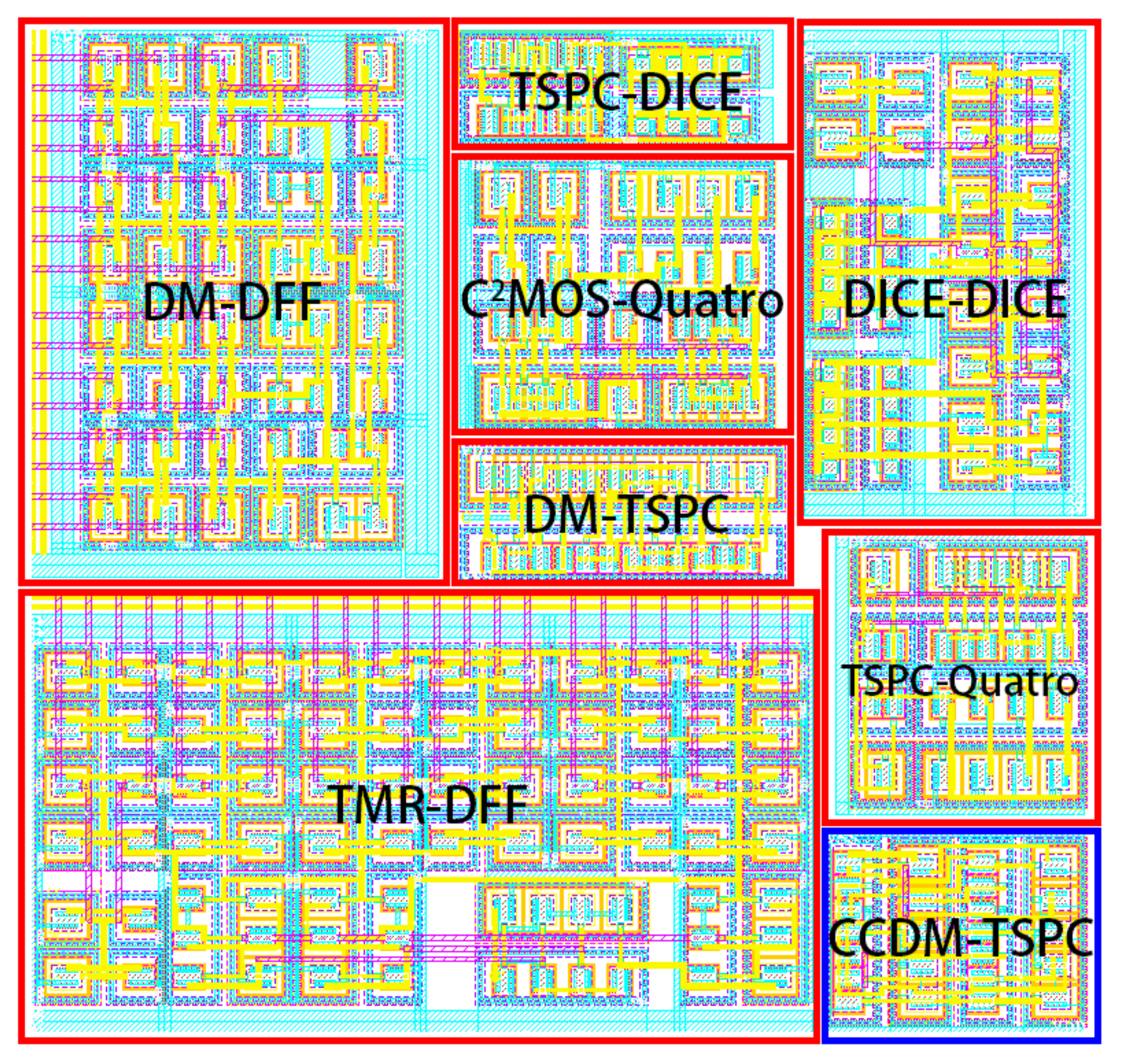
4.5. Layout Area
4.6. SEU Robustness
4.7. Process Variation
5. Conclusions
Author Contributions
Funding
Acknowledgments
Conflicts of Interest
References
- Li, J.; Xiao, L.; Li, H.; Cao, X.; Wang, C. A Soft Error Detection and Recovery Flip-Flop for Aggressive Designs with High-Performance. IEEE Trans. Device Mater. Reliab. 2022, 22, 223–231. [Google Scholar] [CrossRef]
- Alidash, H.K.; Oklobdzija, V.G. Low-power soft error hardened latch. J. Low Power Electron. 2010, 6, 218–226. [Google Scholar] [CrossRef]
- Hamed, E.A.; Lee, I. Categorization and SEU Fault Simulations of Radiation-Hardened-by-Design Flip-Flops. Electronics 2021, 10, 1572. [Google Scholar] [CrossRef]
- Dodd, P.E.; Massengill, L.W. Basic mechanisms and modeling of single-event upset in digital microelectronics. IEEE Trans. Nucl. Sci. 2003, 50, 583–602. [Google Scholar] [CrossRef]
- Teifel, J. Self-voting dual-modular-redundancy circuits for single-event-transient mitigation. IEEE Trans. Nucl. Sci. 2008, 55, 3435–3439. [Google Scholar] [CrossRef]
- Sajjade, F.M.; Goyal, N.K.; Varaprasad, B. Single event transient (SET) mitigation circuits with immune leaf nodes. IEEE Trans. Device Mater. Reliab. 2021, 21, 70–78. [Google Scholar] [CrossRef]
- Farnsworth, C.; Clark, L.T.; Gogulamudi, A.R.; Vashishtha, V.; Gujja, A. A soft-error mitigated microprocessor with software controlled error reporting and recovery. IEEE Trans. Nucl. Sci. 2016, 63, 2241–2249. [Google Scholar] [CrossRef]
- Danilov, I.A.; Gorbunov, M.S.; Antonov, A.A. SET tolerance of 65 nm CMOS majority voters: A comparative study. IEEE Trans. Nucl. Sci. 2014, 61, 1597–1602. [Google Scholar] [CrossRef]
- Lee, H.-H.K.; Klas, L.; Mounaim, B.; Prasanthi, R.; Linscott, I.R.; Inan, U.S.; Subhasish, M. LEAP: Layout design through error-aware transistor positioning for soft-error resilient sequential cell design. In Proceedings of the 2010 IEEE International Reliability Physics Symposium, Anaheim, CA, USA, 2–6 May 2010; pp. 203–212. [Google Scholar]
- Black, J.D.; Black, D.A.; Domme, N.A.; Dodd, P.E.; Griffin, P.J.; Nowlin, R.N.; Trippe, J.M.; Salas, J.G.; Reed, R.A.; Weller, R.A. DFF layout variations in CMOS SOI—Analysis of hardening by design options. IEEE Trans. Nucl. Sci. 2020, 67, 1125–1132. [Google Scholar] [CrossRef]
- Liu, S.; Reviriego, P.; Lombardi, F. Detection of limited magnitude errors in emerging multilevel cell memories by one-bit parity (OBP) or two-bit parity (TBP). IEEE Trans. Emerging Top. Comput. 2019, 9, 1792–1802. [Google Scholar] [CrossRef]
- Li, J.; Xiao, L.; Reviriego, P.; Zhang, R. Efficient implementations of 4-bit burst error correction for memories. IEEE Trans. Circuits Syst. II Express Briefs 2018, 65, 2037–2041. [Google Scholar] [CrossRef]
- Das, A.; Touba, N.A. Efficient one-step decodable limited magnitude error correcting codes for multilevel cell main memories. IEEE Trans. Nanotechnol. 2019, 18, 575–583. [Google Scholar] [CrossRef]
- Zhao, Y.; Wang, L.; Yue, S.; Wang, D.; Zhao, X.; Sun, Y.; Li, D.; Wang, F.; Yang, X.; Zheng, H. SEU and SET of 65 Bulk CMOS Flip-flops and Their Implications for RHBD. IEEE Trans. Nucl. Sci. 2015, 62, 2666–2672. [Google Scholar] [CrossRef]
- Yan, A.; Qian, K.; Cui, J.; Cui, N.; Huang, Z.; Wen, X.; Girard, P. A Highly Reliable and Low Power RHBD Flip-Flop Cell for Aerospace Applications. In Proceedings of the 2022 IEEE 40th VLSI Test Symposium (VTS), San Diego, CA, USA, 25–27 April 2022; pp. 1–6. [Google Scholar]
- Lin, T.; Chong, K.-S.; Shu, W.; Lwin, N.K.Z.; Jiang, J.; Chang, J.S. Experimental investigation into radiation-hardening-by-design (RHBD) flip-flop designs in a 65nm CMOS process. In Proceedings of the 2016 IEEE International Symposium on Circuits and Systems (ISCAS), Montreal, QC, Canada, 22–25 May 2016; pp. 966–969. [Google Scholar]
- Dwivedi, H.K.; Nandi, S.; Lahariya, S.; Nakhate, S. Combinational and sequential standard cell design using Radiation Hardened by Design (RHBD) Technique. In Proceedings of the 2018 International Conference on Advanced Computation and Telecommunication (ICACAT), Bhopal, India, 28–29 December 2018; pp. 1–5. [Google Scholar]
- Wang, H.-B.; Li, Y.-Q.; Chen, L.; Li, L.-X.; Liu, R.; Baeg, S.; Mahatme, N.; Bhuva, B.; Wen, S.-J.; Wong, R. An SEU-tolerant DICE latch design with feedback transistors. IEEE Trans. Nucl. Sci. 2015, 62, 548–554. [Google Scholar] [CrossRef]
- Hatefinasab, S.; Ohata, A.; Salinas, A.; Castillo, E.; Rodriguez, N. Highly Reliable Quadruple-Node Upset-Tolerant D-Latch. IEEE Access 2022, 10, 31836–31850. [Google Scholar] [CrossRef]
- Guo, J.; Liu, S.; Zhu, L.; Lombardi, F. Design and evaluation of low-complexity radiation hardened CMOS latch for double-node upset tolerance. IEEE Trans. Circuits Syst. I Regul. Pap. 2020, 67, 1925–1935. [Google Scholar] [CrossRef]
- Casey, M.C.; Bhuva, B.L.; Black, J.D.; Massengill, L.W.; Amusan, O.A.; Witulski, A.F. Single-event tolerant latch using cascode-voltage switch logic gates. IEEE Trans. Nucl. Sci. 2006, 53, 3386–3391. [Google Scholar] [CrossRef]
- Wang, H.-B.; Chen, L.; Liu, R.; Li, Y.-Q.; Kauppila, J.; Bhuva, B.; Lilja, K.; Wen, S.-J.; Wong, R.; Fung, R. An area efficient stacked latch design tolerant to SEU in 28 nm FDSOI technology. IEEE Trans. Nucl. Sci. 2016, 63, 3003–3009. [Google Scholar] [CrossRef]
- Wang, H.-B.; Bi, J.-S.; Li, M.-L.; Chen, L.; Liu, R.; Li, Y.-Q.; He, A.-L.; Guo, G. An area efficient SEU-tolerant latch design. IEEE Trans. Nucl. Sci. 2014, 61, 3660–3666. [Google Scholar] [CrossRef]
- Li, Y.-Q.; Wang, H.-B.; Liu, R.; Chen, L.; Nofal, I.; Shi, S.-T.; He, A.-L.; Guo, G.; Baeg, S.; Wen, S.-J. A quatro-based 65-nm flip-flop circuit for soft-error resilience. IEEE Trans. Nucl. Sci. 2017, 64, 1554–1561. [Google Scholar] [CrossRef]
- Katkar, P.; Kumar, S.S.; Kumaravel, S. SEU hardened DFF and 4 bit johnson counter using quatro latch in 45 nm technology. In Proceedings of the 2017 International conference on Microelectronic Devices, Circuits and Systems (ICMDCS), Vellore, India, 10–12 August 2017; pp. 1–6. [Google Scholar]
- Lyons, R.E.; Vanderkulk, W. The use of triple-modular redundancy to improve computer reliability. IBM J. Res. Dev. 1962, 6, 200–209. [Google Scholar] [CrossRef]
- Furuta, J.; Hamanaka, C.; Kobayashi, K.; Onodera, H. A 65nm Bistable Cross-coupled Dual Modular Redundancy Flip-Flop capable of protecting soft errors on the C-element. In Proceedings of the 2010 Symposium on VLSI Circuits, Honolulu, HI, USA, 16–18 June 2010; pp. 123–124. [Google Scholar]
- Shaikh, J.; Rahaman, H. High speed and low power preset-able modified TSPC D flip-flop design and performance comparison with TSPC D flip-flop. In Proceedings of the 2018 International Symposium on Devices, Circuits and Systems (ISDCS), Howrah, India, 29–31 March 2018; pp. 1–4. [Google Scholar]
- Li, H.; Zhang, Y.; Yoshihara, T. Clocked CMOS adiabatic logic with low-power dissipation. In Proceedings of the 2013 International SoC Design Conference (ISOCC), Busan, Korea, 17–19 November 2013; pp. 064–067. [Google Scholar]
- Black, D.A.; Robinson, W.H.; Wilcox, I.Z.; Limbrick, D.B.; Black, J.D. Modeling of single event transients with dual double-exponential current sources: Implications for logic cell characterization. IEEE Trans. Nucl. Sci. 2015, 62, 1540–1549. [Google Scholar] [CrossRef]
- Tian, H.; Yang, H.; Ma, X.; He, S. Design of radiation hardened master-slave type flip-flop based on DICE. Weidianzixue (Microelectron.) 2013, 43, 65–69. [Google Scholar]
- Petrovic, V.; Krstic, M. Design flow for radhard TMR Flip-Flops. In Proceedings of the 2015 IEEE 18th International Symposium on Design and Diagnostics of Electronic Circuits & Systems, Belgrade, Serbia, 22–24 April 2015; pp. 203–208. [Google Scholar]
- Jaya, G.L.; Chen, S.; Liter, S. A dual redundancy radiation-hardened Flip-Flop based on C-element in 65nm process. In Proceedings of the 2016 International Symposium on Integrated Circuits (ISIC), Singapore, 12–14 December 2016; pp. 1–4. [Google Scholar]
- Gupta, S.; Mekie, J. Soft error resilient and energy efficient dual modular TSPC flip-flop. In Proceedings of the 2019 32nd International Conference on VLSI Design and 2019 18th International Conference on Embedded Systems (VLSID), Delhi, India, 5–9 January 2019; pp. 341–346. [Google Scholar]
- Jahinuzzaman, S.M.; Rennie, D.J.; Sachdev, M. Soft error robust impulse and TSPC flip-flops in 90nm CMOS. In Proceedings of the 2009 2nd Microsystems and Nanoelectronics Research Conference, Ottawa, ON, Canada, 13–14 October 2009; pp. 45–48. [Google Scholar]
- Rennie, D.J.; Sachdev, M. Novel soft error robust flip-flops in 65nm cmos. IEEE Trans. Nucl. Sci. 2011, 58, 2470–2476. [Google Scholar] [CrossRef]
- Jahinuzzaman, S.M.; Islam, R. TSPC-DICE: A single phase clock high performance SEU hardened flip-flop. In Proceedings of the 2010 53rd IEEE International Midwest Symposium on Circuits and Systems, Seattle, WA, USA, 1–4 August 2010; pp. 73–76. [Google Scholar]
- Choi, J.-S.; Lee, K. Design of CMOS tapered buffer for minimum power-delay product. IEEE J. Solid-State Circuits 1994, 29, 1142–1145. [Google Scholar] [CrossRef]


| Number of Transistors | C-Q Delay (ns) | Power (mW) | PDP (pJ) | Layout Area (μm2) | Single-Phase Clock * | SEU Robustness | |
|---|---|---|---|---|---|---|---|
| DICE-DICE [31] | 36 | 0.86 | 3.72 | 15.51 | 1144 | × | OK |
| TMR-DFF [32] | 78 | 0.50 | 3.08 | 11.77 | 2880 | × | OK |
| DM-DFF [33] | 46 | 0.50 | 2.72 | 10.14 | 1850 | × | OK |
| DM-TSPC [34] | 22 | 0.21 | 2.62 | 8.47 | 390 | √ | No |
| TSPC-Quatro [35] | 25 | 0.29 | 3.18 | 10.93 | 598 | √ | No |
| C2MOS-Quatro [36] | 30 | 0.34 | 2.70 | 10.76 | 754 | × | No |
| TSPC-DICE [37] | 22 | 0.23 | 2.65 | 9.36 | 319 | √ | Poor |
| CCDM-TSPC | 24 | 0.13 | 2.61 | 8.47 | 456 | √ | OK |
Publisher’s Note: MDPI stays neutral with regard to jurisdictional claims in published maps and institutional affiliations. |
© 2022 by the authors. Licensee MDPI, Basel, Switzerland. This article is an open access article distributed under the terms and conditions of the Creative Commons Attribution (CC BY) license (https://creativecommons.org/licenses/by/4.0/).
Share and Cite
Wang, S.; Wang, L.; Wang, Y.; Guo, M.; Li, Y. A Novel Radiation-Hardened CCDM-TSPC Compared with Seven Well-Known RHBD Flip-Flops in 180 nm CMOS Process. Electronics 2022, 11, 3098. https://doi.org/10.3390/electronics11193098
Wang S, Wang L, Wang Y, Guo M, Li Y. A Novel Radiation-Hardened CCDM-TSPC Compared with Seven Well-Known RHBD Flip-Flops in 180 nm CMOS Process. Electronics. 2022; 11(19):3098. https://doi.org/10.3390/electronics11193098
Chicago/Turabian StyleWang, Shixin, Lixin Wang, Yue Wang, Min Guo, and Yuanzhe Li. 2022. "A Novel Radiation-Hardened CCDM-TSPC Compared with Seven Well-Known RHBD Flip-Flops in 180 nm CMOS Process" Electronics 11, no. 19: 3098. https://doi.org/10.3390/electronics11193098
APA StyleWang, S., Wang, L., Wang, Y., Guo, M., & Li, Y. (2022). A Novel Radiation-Hardened CCDM-TSPC Compared with Seven Well-Known RHBD Flip-Flops in 180 nm CMOS Process. Electronics, 11(19), 3098. https://doi.org/10.3390/electronics11193098