1. Introduction
High power microwave (HPM) technology is being actively explored [
1,
2,
3,
4] and has achieved significant importance in both military and commercial applications [
5]. The selection of antenna elements is very important in the HPM system to achieve good far-field radiation characteristics along with high power handling capability [
6]. The HPM antennas are usually deployed at the end terminal device of the HPM system. Slotted waveguide antennas (SWAs) are mostly used in HPM applications, which include radar navigation and communication [
7]. These SWA systems are attractive due to their high-gain/directivity, simplicity of design, robustness, light-weight, good reflection coefficient, and high-power handling capability [
8]. SWAs are commonly made of rectangular waveguides. In SWA, slots are cut on the broad wall or narrow wall of the waveguide to radiate the electromagnetic energy in the targeted direction [
9]. The most common slot types include longitudinal broad wall slots, inclined edge or sidewall slots, and cross-slot configuration [
6,
10].
The SWAs are generally divided into two categories: resonant (standing-wave) and non-resonant (traveling-wave) antennas. The resonant SWAs are preferred to their complements due to short-circuit termination, which increases their efficiency without power loss. The resonant SWA configuration provides a normal beam in the targeted direction, which is independent of resonant frequency. However, the main limitation of resonant SWA is its narrow bandwidth. Traveling-wave SWAs have a wide impedance bandwidth but low efficiency due to the presence of a matched load to prevent wave reflection. In addition, a significant phase difference is realized between the radiating slots. The main beam direction is also frequency-dependent [
5,
11]. The most effective technologies to improve the radiation performance of slotted antennas include: electromagnetic band gap (EBG) structures [
12], electromagnetic metasurface [
13], frequency selective surface (FSS) [
14], partially reflecting surface (PRS) [
15], dielectric radome, and corrugated groove structures [
16]. The performance of the SWA configuration in this manuscript is enhanced by using modified Gaussian slot distribution, inside-groove, and dielectric radomes. The inside-groove structures are usually placed around the slotted region to enhance the beaming effect in the SWAs. In addition, corrugated structures also suppress surface wave propagation [
17]. The corrugation in the slotted aperture results in the re-distribution of electromagnetic waves, reflecting high field strength in the grooved surface and re-radiating the waves in the free space region as a secondary source [
18]. A rectangular SWA configuration combined with a one-dimensional (1D) corrugated periodic groove is reported in [
19]. The radiation performance of conventional antenna systems is enhanced by incorporating four periodic corrugated groove structures. The corrugated groove period, width, and depth play an important role in controlling the SWA performance and suppression of back-lobe.
In [
20], a high-gain in SWA is attained by integrating the inside-groove structure along with a single FSS. The addition of identical grooves on both sides of the SWA aperture provides a measured peak gain of 15.1 dBi. Moreover, the addition of a symmetric groove reduces the half-power beamwidth (HPBW) in a single plane to contribute to high gain achievement. Another antenna configuration with a periodic groove arrangement is used to obtain a significant improvement in gain [
21]. The authors utilized six multiple grooves in the waveguide aperture to enrich the radiation performance. The six pairs of grooves on the narrow slit provide a gain of 11 dBi and offer a narrow beamwidth in the E-plane. In another study [
16], a symmetric groove arrangement was applied on both sides of the slots to achieve a gain enhancement of 9 dBi. Additionally, the non-grooved region in SWA is covered with a high dielectric medium to achieve a high gain. However, SLLs are degraded due to the presence of high dielectric medium, which disturbs the surface current propagation. The inside-groove structures in the SWA system are used to enhance the isolation of array elements [
22].
The distribution of slots in the SWA configuration is very important to controlling the far-field radiation characteristics. The window distribution can be categorized into uniform and non-uniform distributions. The uniform distribution in the array configuration provides high sidelobe levels (SLLs), which are undesirable in military and defense applications. Therefore, non-uniform distribution is required to improve the radiation characteristics in the single element and array configuration. Different types of non-uniform distributions include but are not limited to: Chebyshev, Taylor, and Binomial, etc. These window distributions are applied in slotted waveguides to achieve the desired SLL in H-plane [
10]. In this paper, a modified Gaussian window distribution has been designed and investigated to achieve the lowest possible SLLs. For the proposed SWA, the window function is designed in such a way that it provides an SLL of less than 20 dB in the H-plane.
The performance parameters of SWA are typically influenced by the radome shape, position, and dielectric material [
23,
24]. Therefore, electromagnetic analysis of the radome structure combined with the SWA system is required to overcome the degradation effect in far-field characteristics. In addition, the HPM antennas are usually sealed properly to protect them from environmental effects and to pressurize them for high power handling capability [
5,
25,
26]. Therefore, to achieve the desired milestones (high gain and high-power handling capability), the Gaussian dielectric radome must be designed, sealed properly, and pressurized. The radome structure used in the proposed design contributes to dual-purpose, i.e., high power handling capability and radiation pattern improvement without affecting the other performance parameters.
In this manuscript, an improved high-gain SWA system with inside-groove and Gaussian dielectric radome is designed for HPM applications. The use of the inside-groove structure offers a gain enhancement of 3.63 dBi, while the use of modified Gaussian slot distribution offers SLLs of less than 20 dB in both principal radiation planes. Moreover, a dielectric radome is placed over the SWA aperture for sealing and pressurizing to be compatible with the HPM applications without affecting the other antenna performance parameters. The proposed SWA system has been designed and analyzed by using the commercially available CST Microwave Studio 2019. The rest of the manuscript is organized as follows:
Section 2 briefly outlines the design configuration and analysis of slot-position, shape, and displacement. The analysis of modified Gaussian slot distribution along with Gaussian dielectric radome is also discussed in this section. The simulated results are elaborated in
Section 3.
Section 4 presents the parametric analysis of the proposed SWA system. The fabrication process and measured results are discussed in
Section 5. Finally, the manuscript is concluded in
Section 6.
2. Design and Analysis of SWA System
In this section, SWA layout and design configuration are discussed.
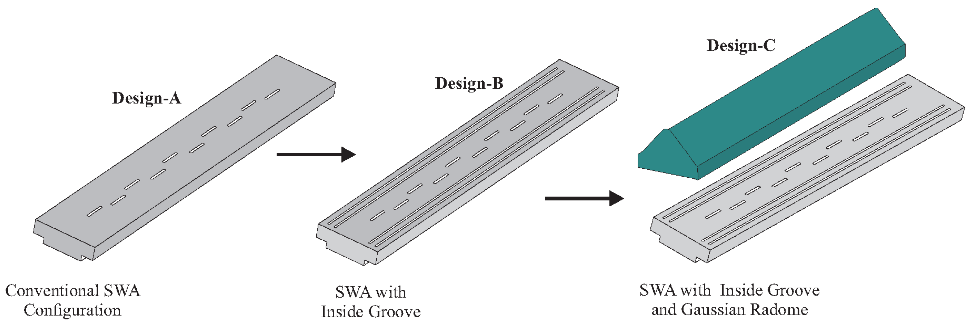
Figure 1 shows the design configuration of the SWA with a Gaussian radome and an inside-groove structure. First, a conventional SWA system is designed by using a modified Gaussian slot distribution. In the second step, inside-grooves are introduced in the design to achieve high gain and low SLLs. In the last, a high-density polyethylene (HDPE) Gaussian radome is placed on the designed SWA system to be compatible with HPM applications without affecting the performance parameters. The placement of a Gaussian radome further enhances the gain of the antenna system to some extent.
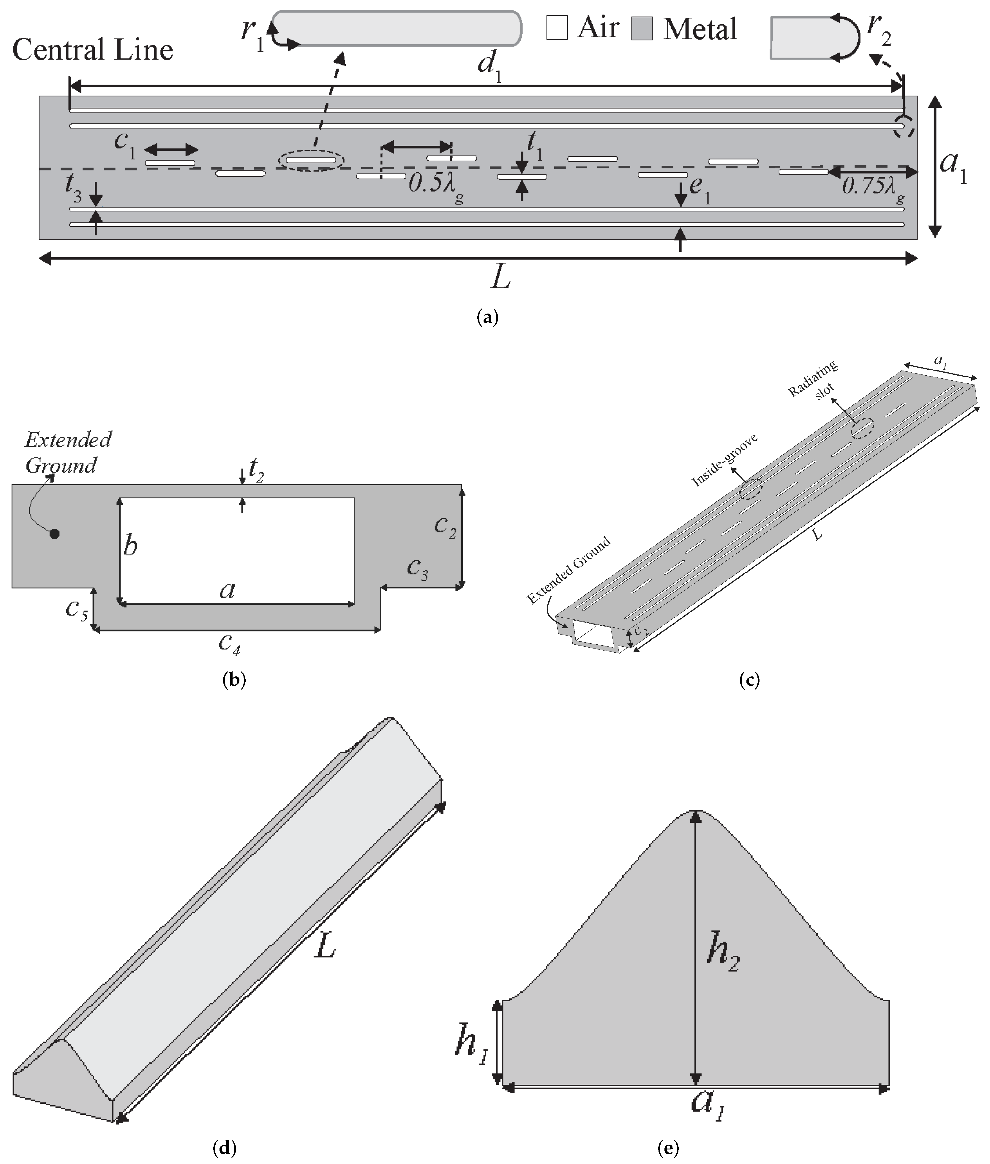
A systematic design procedure is followed in the SWA system to achieve the desired SLLs at the 3 GHz frequency band. Initially, the dimensions and positions of all radiating slot elements are determined. A modified Gaussian slot distribution is used to find the displacements of all slots from the central line of the waveguide (see
Figure 2a) to attain the desired SLL values. The WR-284 waveguide, operating in the S-band (2–4 GHz) and resonating at 3 GHz, is used to achieve the intended milestones. A standard WR-284 waveguide has dimensions of
a = 2.84” and
b = 1.37”. The waveguide structure is fed from one side (see
Figure 2b), while the other end is terminated properly [
5,
27,
28].
Initially, the conventional SWA configuration with 10-slots is employed to achieve the desired gain, as shown in
Figure 2a. The radiation performance of conventional SWA can be improved with structural modification to radiate efficiently in the E-plane. For this purpose, inside-groove structures (see
Figure 2c) are integrated on the broad wall around the main radiating region. These corrugated structures suppress the unwanted surface currents, resulting in the re-distribution of electromagnetic waves in the targeted direction. This radiating secondary source creation improves the overall radiation performance of the SWA system. After that, a dielectric Gaussian radome, as shown in
Figure 2d,e, is installed to be compatible with HPM applications without affecting the performance parameters and also enhance the gain of the antenna system. The rest of the overall design parameters are listed in
Table 1, while the complete design procedure is provided in the following subsections.
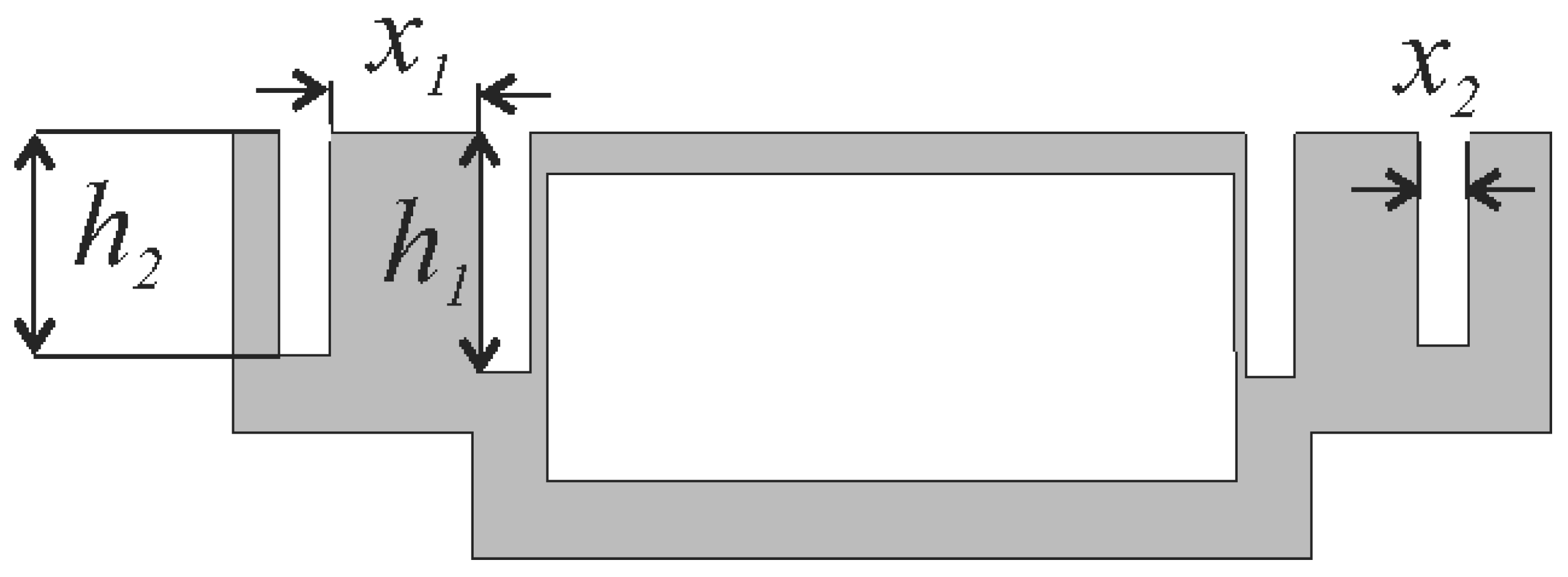
2.1. Position of Longitudinal Slot
The following steps are taken into consideration for slots’ placement on the broadside wall of the waveguide: the first slot is placed at a distance of 3
/4 from the feeding point (see
Figure 2a) and all other slots are placed at a distance of
/2, as shown in
Figure 1a. For SWA design, the guided wavelength (
) is calculated as follows:
where
and
are the operating and cut-off wavelengths of SWA, respectively.
c is the speed of light and
f is the resonant frequency. For the desired resonant frequency (3 GHz),
= 138.5 mm. For the longitudinal slot configuration, the waveguide acts as a transmission line model. Therefore, by employing the concept of a transverse electric field in each slot, TE
10 mode scattering is considered to be symmetrical in this configuration [
5,
10,
28].
2.2. Shape and Dimensions of Slot
The shape and geometry of the slot play an important role in the design of the HPM antenna. The conventional rectangular slot configuration integrated with the HPM source could heighten electrical breakdown problems due to electric field enhancement at sharp corners [
10]. This rapid field enhancement in the slotted region can lead to self-induced microwave breakdown of the air in the slot. Therefore, sharp corners are avoided to overcome this issue in HPM applications. A round-edged slot configuration (see
Figure 3) was chosen to improve the power handling capability with less manufacturing difficulty compared to the rectangular slot (sharp 90
angle at corners). In the round-edged slot configuration, the length is optimized to obtain the desired reflection coefficient in the 3 GHz frequency band. The width of the slot in the round-edged configuration in our design is taken to be equal to
/10 due to design limitations related to available fabrication limitations. The thickness of the upper slotted plate is 3 mm, according to which specific slot thickness is considered to obtain a good impedance match at the desired frequency band [
5,
9,
27,
28,
29].
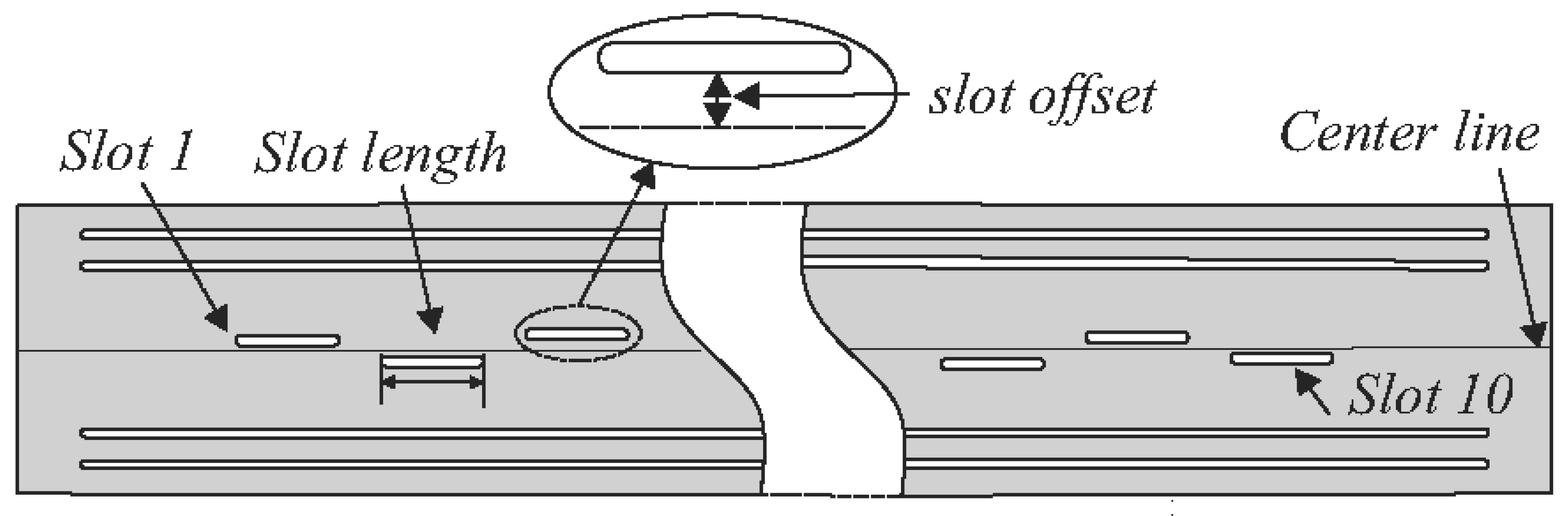
2.3. Slot Offset
The slot offset plays an important role in controlling the SLLs of the SWA system. The distance between the broad wall centre-line and the slot-centre is indicated as the slot offset. There are two types of slot distribution: uniform and non-uniform. In uniform distribution, all slots are placed at the same offset from the central line and have equal excitations for all elements in the antenna array. The uniform distribution is easier to implement with a similar offset distance, but the major drawback is the higher SLLs in the array configuration. Therefore, non-uniform slot displacement is preferred to control the SLLs in the array configuration [
10].
All the slot elements in SWA should radiate in phase to obtain higher efficiency. Therefore, slots are deployed in an alternating order on the broad side wall of the SWA around the central-line (see
Figure 2a and
Figure 3) [
30,
31]. The non-uniform slot distribution approach for desired SLLs and slot displacement is illustrated in
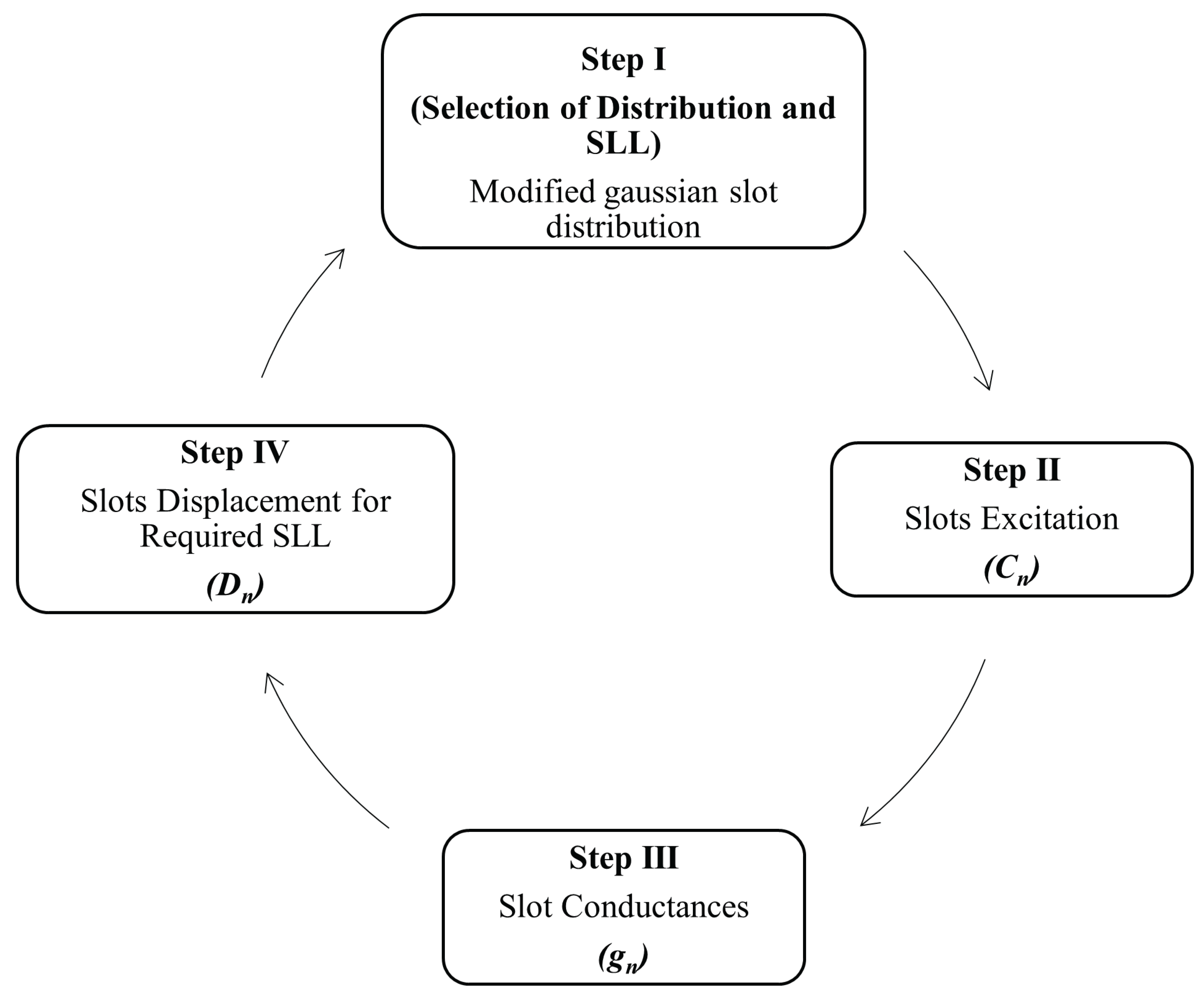
Figure 4. The slot displacements around the central line are calculated as follows: Firstly, required SLL values are chosen, and then slot conductance is determined using a modified Gaussian slot distribution. The obtained slot conductance is used to extract the value of slot displacement from the central line. The slot displacements basically control the excitation of every slot and are also used to control the SLL value of the entire SWA system. In [
30,
32], different window functions, including Chebyshev, Taylor, and Binomial, have been implemented for specific SLLs in SWA design. In our proposed design configuration, a modified Gaussian window is chosen to calculate the slot displacement. The modified Gaussian curve is defined by the following equation:
where
,
N denotes number of points for Gaussian distribution, and
represents SLL controlling parameter.
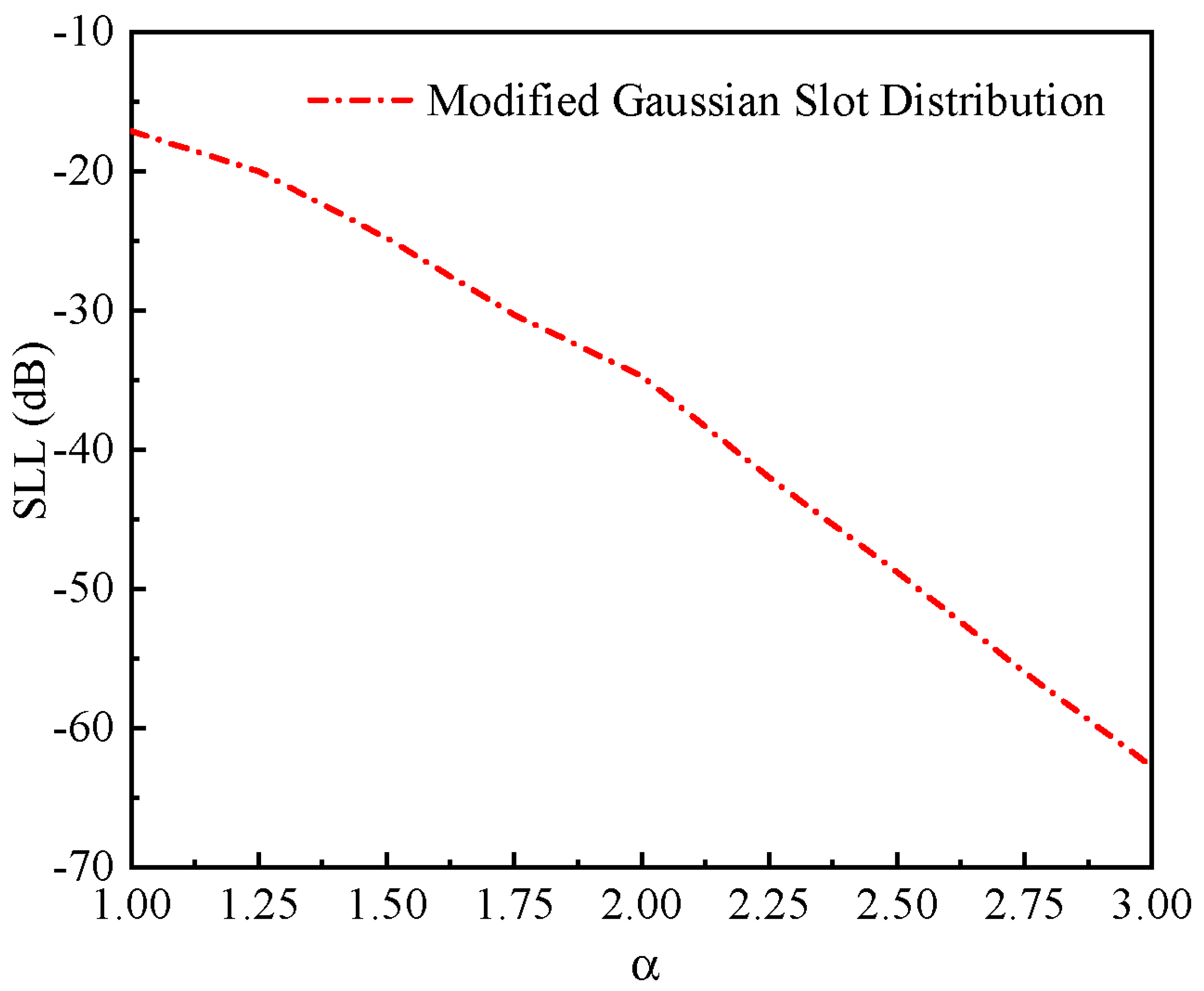
Initially, a modified Gaussian window has been analyzed to generate different SLL values with the controlling parameter (
), as shown in
Figure 5. The Gaussian window distribution is optimized for 10-slots in SWA to achieve the desired SLL in the H-plane. By using the obtained Gaussian coefficients (listed in
Table 2), an SLL value of −46.5 dB, which is 8 dB lower as compared to the Binomial distribution (−38.8 dB SLL), with the same gain value of 15 dB being achieved [
10,
33]. The slot displacements against these coefficients are obtained by using Equations (
3) and (
4) [
5,
23,
30,
31], and are listed in
Table 2. The proposed modified SWA simulations have been performed in CST Microwave Studio, which provides −19.5 dB SLLs and a gain of 16.5 dBi with a reflection coefficient of −32 dB. The proposed SWA gain performance with other reported distributions (uniform, Chebyshev, Taylor, and Binomial) in [
10] is compared in
Table 3 and
Table 4:
where
2.4. Design of Inside-Groove Structure
The inside-groove structures are usually deployed around the slotted region to enhance the radiation performance of the conventional SWA system. The grooves are mostly used to re-radiate the surface wave radiation and suppress surplus surface currents at the extended ground edge of the SWA aperture. The edge diffraction currents are suppressed in the grounded region due to the presence of corrugated inner grooves around the slots. The dimensions of the grooving structure are very important to controlling the radiation performance. The radiation performance depends on the following parameters, which include: periodicity, depth, width, and length of grooving structure. The first groove is placed at the wall of the waveguide U-channel at 0.56
distance from the centre of the waveguide (see
Figure 6) having a length of 8.71
, depth of
= 0.23
, and a width of
= 0.04
. The second groove is located 0.65
from the center, 0.0761
from the first groove, and has a length of 8.71
, a depth of
= 0.208
, and a width of
= 0.04
, as shown in
Figure 6.
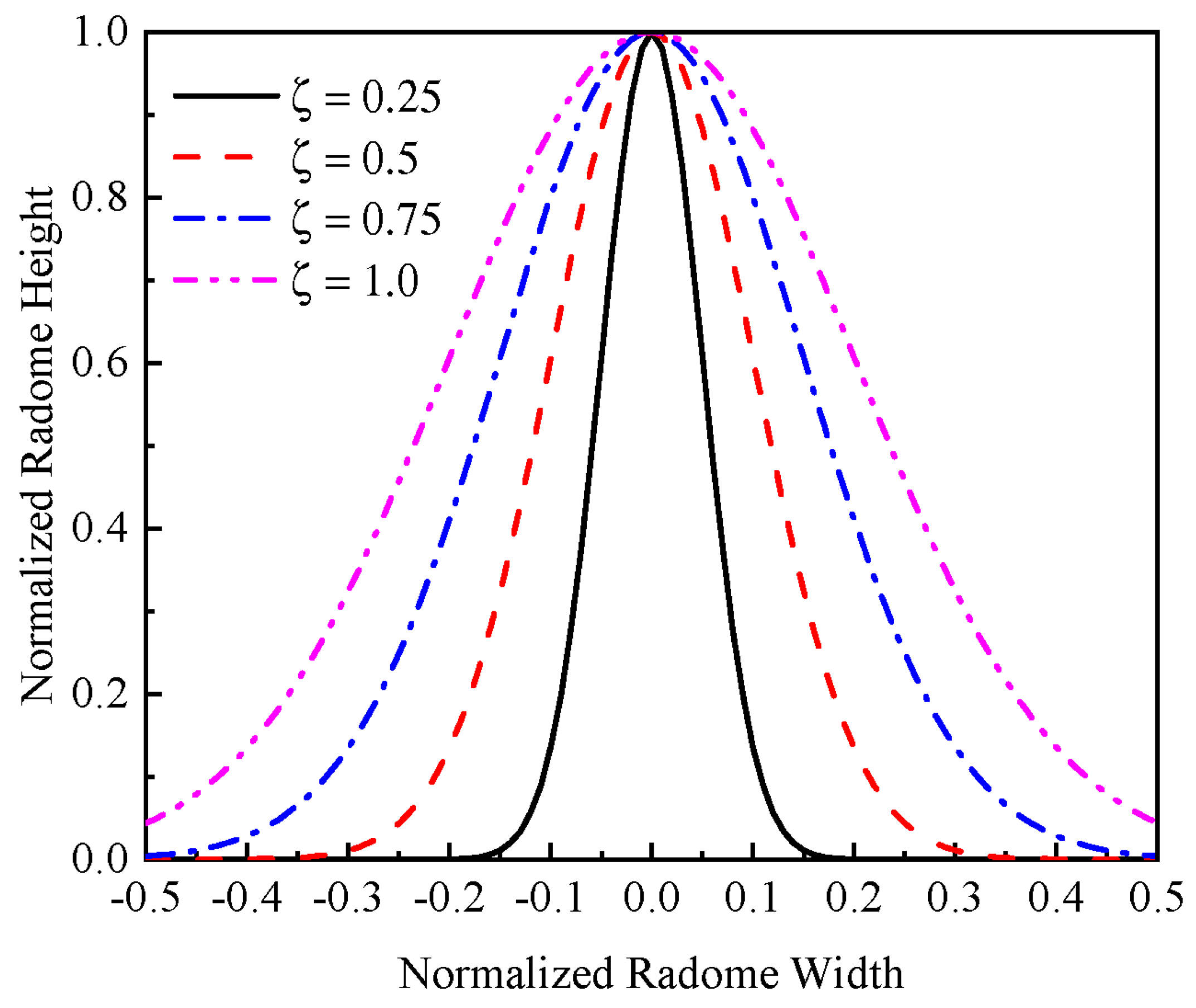
2.5. Design of Dielectric Gaussian Radome
A transparent radio frequency (RF) radiation dielectric radome is mostly placed on the SWA aperture in the HPM antenna design to contain vacuum or pressurized gas (
or
) for HPM capability. This dielectric enclosure protects the antenna aperture from external environmental effects, including dust, moisture, and rain. Moreover, the dielectric enclosure also provides aerodynamic support. To fulfill these required milestones, a Gaussian-profiled dielectric radome has been designed, which has the clear advantages of gain enhancement and beamwidth suppression in the E-plane without affecting the reflection coefficient and radiation characteristics. The dielectric enclosure is used for the sealing of the 10-slot SWA aperture to hold the vacuum or pressurized to enhance E-field breakdown strength [
34,
35,
36]. The dielectric radome is based on the Gaussian function and can be defined as:
where
,
h is the height of the dielectric enclosure,
l denotes the width of the profile, and
represents the beam shaping parameter.
The analysis of
for normalized height and width is shown in
Figure 7. The radiated electromagnetic waves may be converged or diverged with the effect of diffraction based on the curvature profiling and thickness of the dielectric material. In the proposed design, a dielectric Gaussian radome is designed to converge the electromagnetic waves in the targeted direction at a height of 100 mm. The dielectric Gaussian-profiled curvature and thickness are optimized with the objective of improving the radiation patterns (i.e., gain enhancement and beamwidth reduction) along with vacuum/pressurized gas sealing for HPM capability without affecting the reflection coefficient. The HDPE dielectric material has been used for radome design with a dielectric constant of 2.1. The following parameters are chosen for the radome:
h = 100 mm,
l = 138.14 mm, and
= 0.95 with a thickness of 30 mm.
3. Simulation Results and Discussion
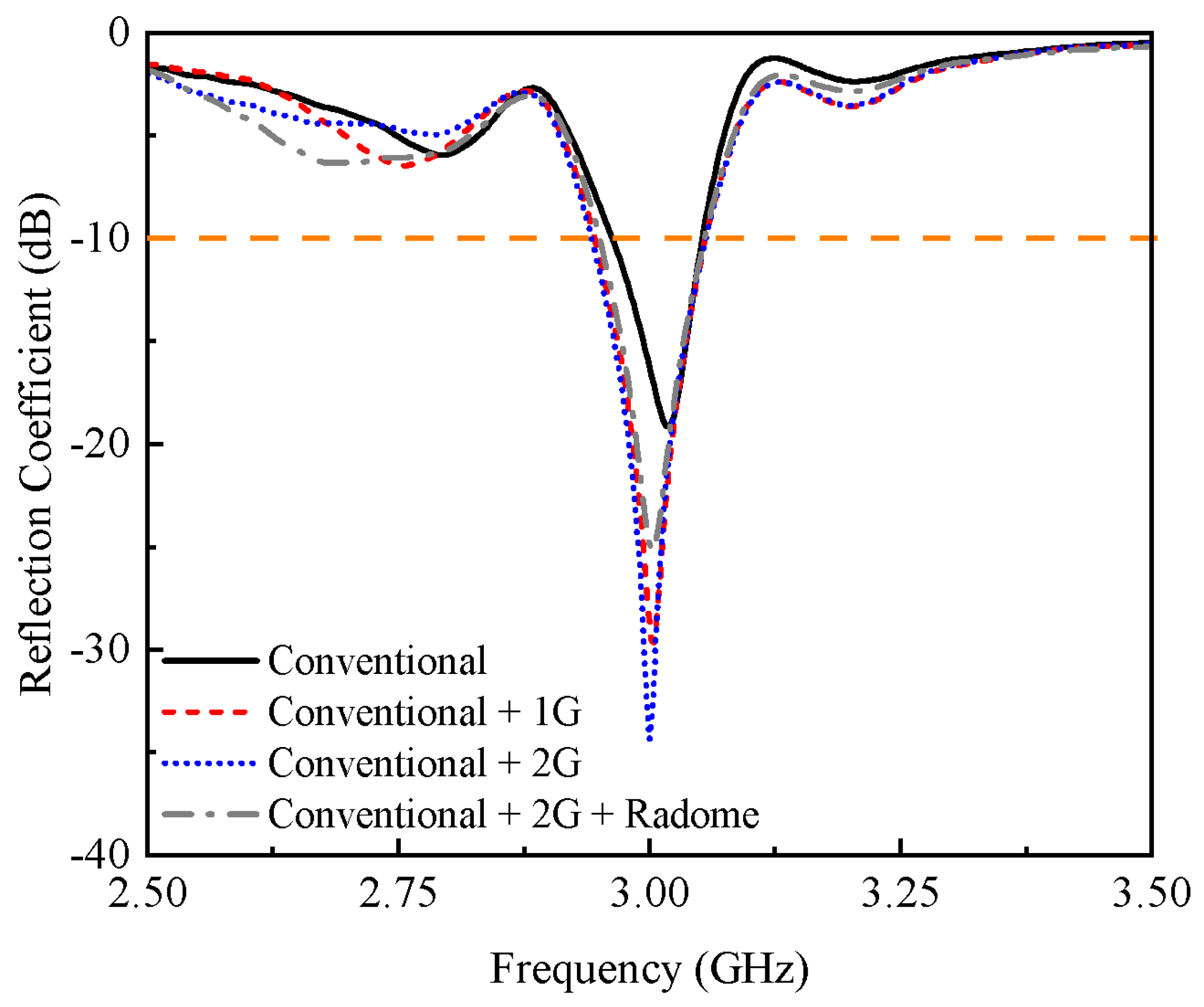
The performance of a modified SWA configuration with inside-groove and dielectric radome is studied in terms of reflection coefficient, surface current distribution, and far-field radiation characteristics. The conventional SWA configuration provides a dip at 3 GHz with a reflection coefficient of −17 dB. The grooving region in the SWA is used for a dual purpose: to achieve better impedance matching along with gain enhancement. The proposed SWA system design methodology is shown in
Figure 1, and the corresponding reflection coefficient for each design step is demonstrated in
Figure 8. The addition of the first and second groove on the SWA broadside aperture improves the reflection coefficient from −17 dB to −35 dB. The dielectric radome is very important in HPM systems to pressurize the waveguide for HPM capability. The HDPE-based Gaussian-shaped dielectric radome is used for pressurization. The reflection coefficient of SWA is not shifted by applying the dielectric radome. However, the reflection coefficient magnitude is decreased by up to −25 dB by installing the dielectric radome.
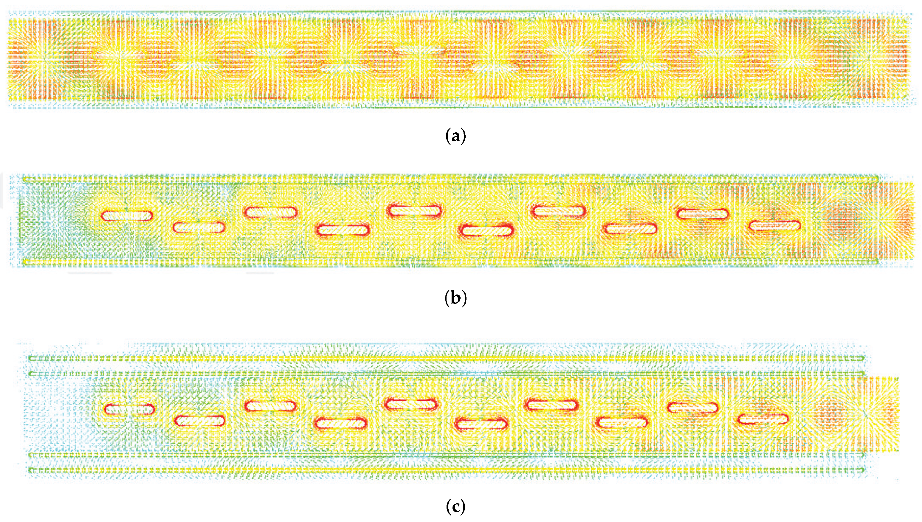
The surface current distribution of a 10-slot configuration with one and two grooves is illustrated in
Figure 9. In the conventional SWA configuration, currents are converged and dominate around the slotted region. It can be seen that the current in the groove structure is strongly concentrated in the centre compared to the conventional SWA system. High surface currents are now localized around the edges of the slots in the modified geometry with 2-grooves. Moreover, a high current region is also observed inside the grooves. These high densities with localized current regions increase the gain of the proposed geometry from 16.4 dBi to 18.9 dBi. Due to the high-density localized currents around the slots and grooved region, the gain of the grooved integrated SWA increased, whereas the SLL was significantly reduced. The comparison of conventional SWA in terms of design methodology is given in
Table 5.
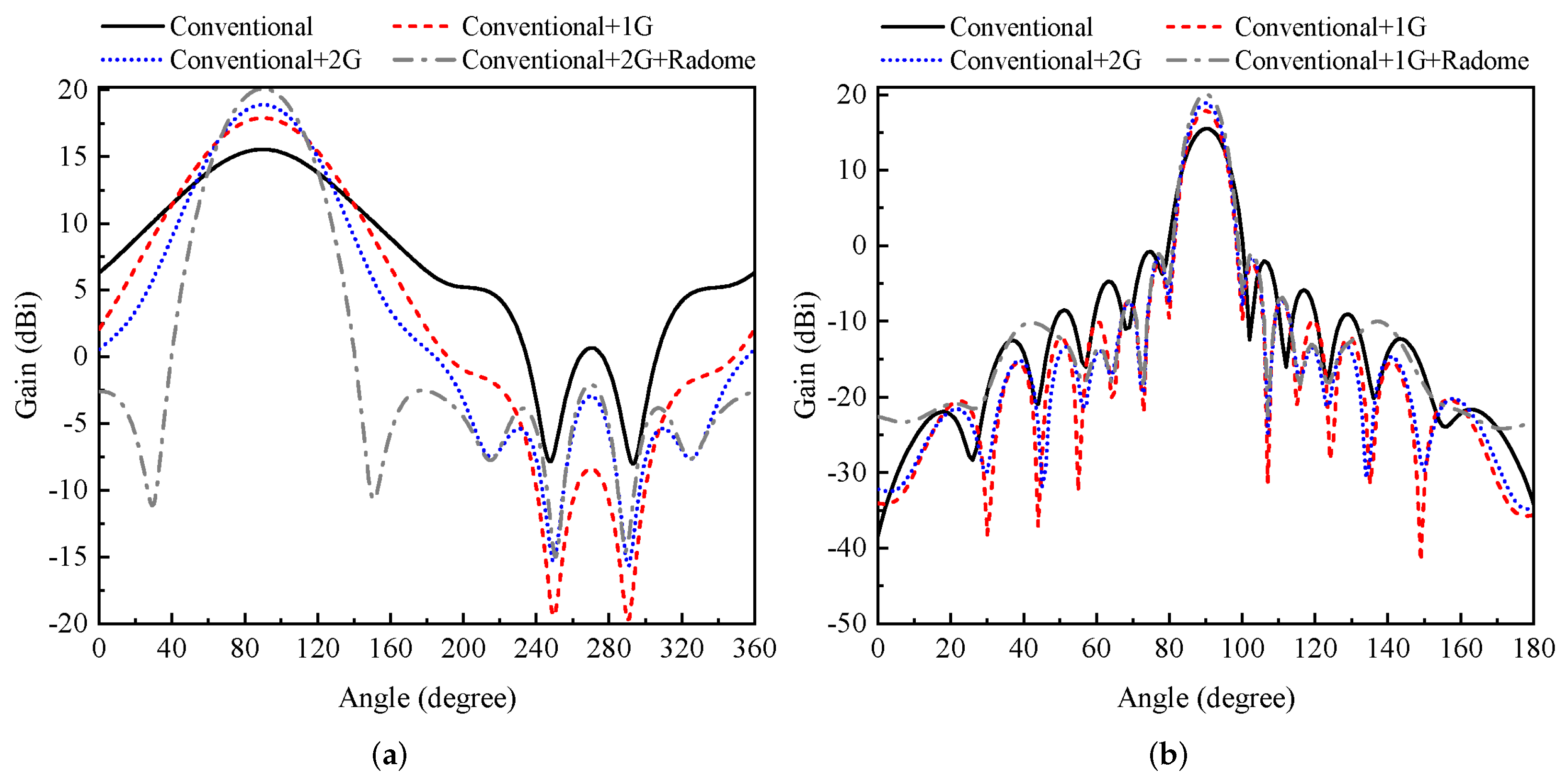
The far-field E- and H-plane radiation characteristics of the proposed SWA system are shown in
Figure 10. The addition of the 1st and 2nd groove enhances the gain and reduces the E-plane beamwidth. The E-plane of SWA is controlled by the structural changes (groove integration). Moreover, the addition of a dielectric radome increases the gain and directivity of the proposed SWA configuration. It is also possible to see that the radiation pattern has a confined beam in the desired direction with no significant side-lobes or back-lobes before and after the radome installation. The conventional SWA offers a gain of 16.4 dBi, which is further enhanced up to 18.9 dBi (see
Figure 10) with the help of inside-grooves. The dielectric Gaussian radome at the end is placed on the SWA aperture for beam shaping without affecting the other SWA performance parameters. The dielectric radome provides gain enhancement of 1.2 dB (see
Figure 10) along with an E-plane beamwidth reduction of about 10
, as shown in
Figure 10a. Furthermore, there is no or minimal effect observed in the beamwidth of the H-plane radiation pattern, as shown in
Figure 10b. The change in gain value and beamwidth is also listed in
Table 5.
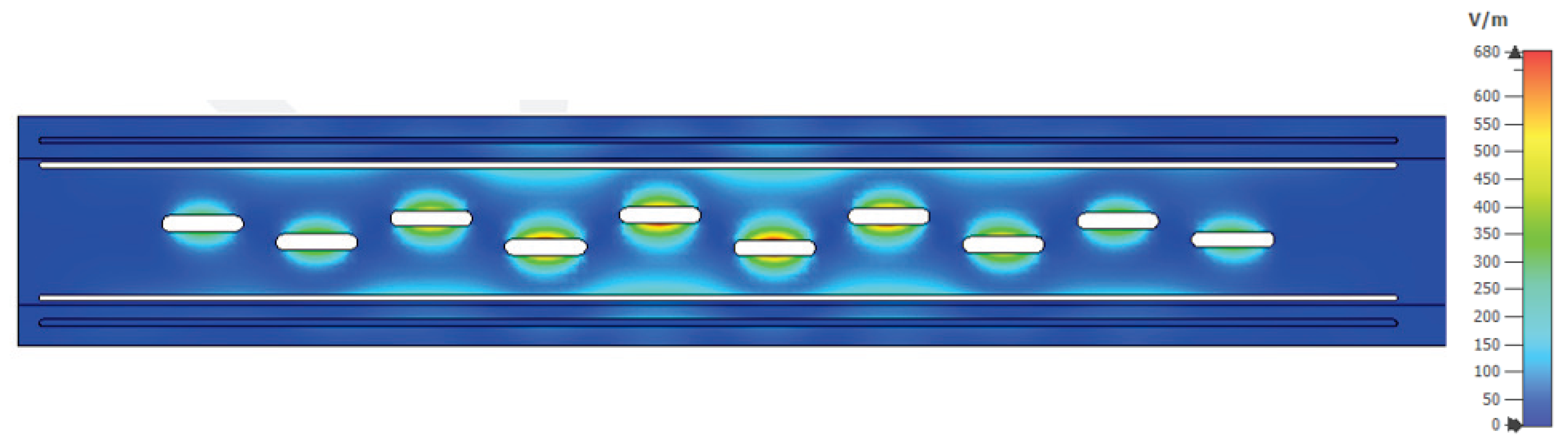
The power handling capability of the SWA system integrated with inside-grooves is estimated to be able to withstand the electrical breakdown. To calculate the power handling capability, the electric field distribution on the aperture of the SWA system is simulated and illustrated in
Figure 11. The maximum electric field intensity on the aperture is 680 V/m when the structure is excited with 0.5 W of input power. According to the square relationship between power
P and field intensity
E, the power capability can be calculated as follows:
where
represents vacuum breakdown threshold of 10 MV/m in the S-band,
is the maximum
E field intensity (680 V/m), and
is the input power (0.5 W). Numerical analysis indicates that the power capacity of the whole SWA with groove structure is more than 100 MW.
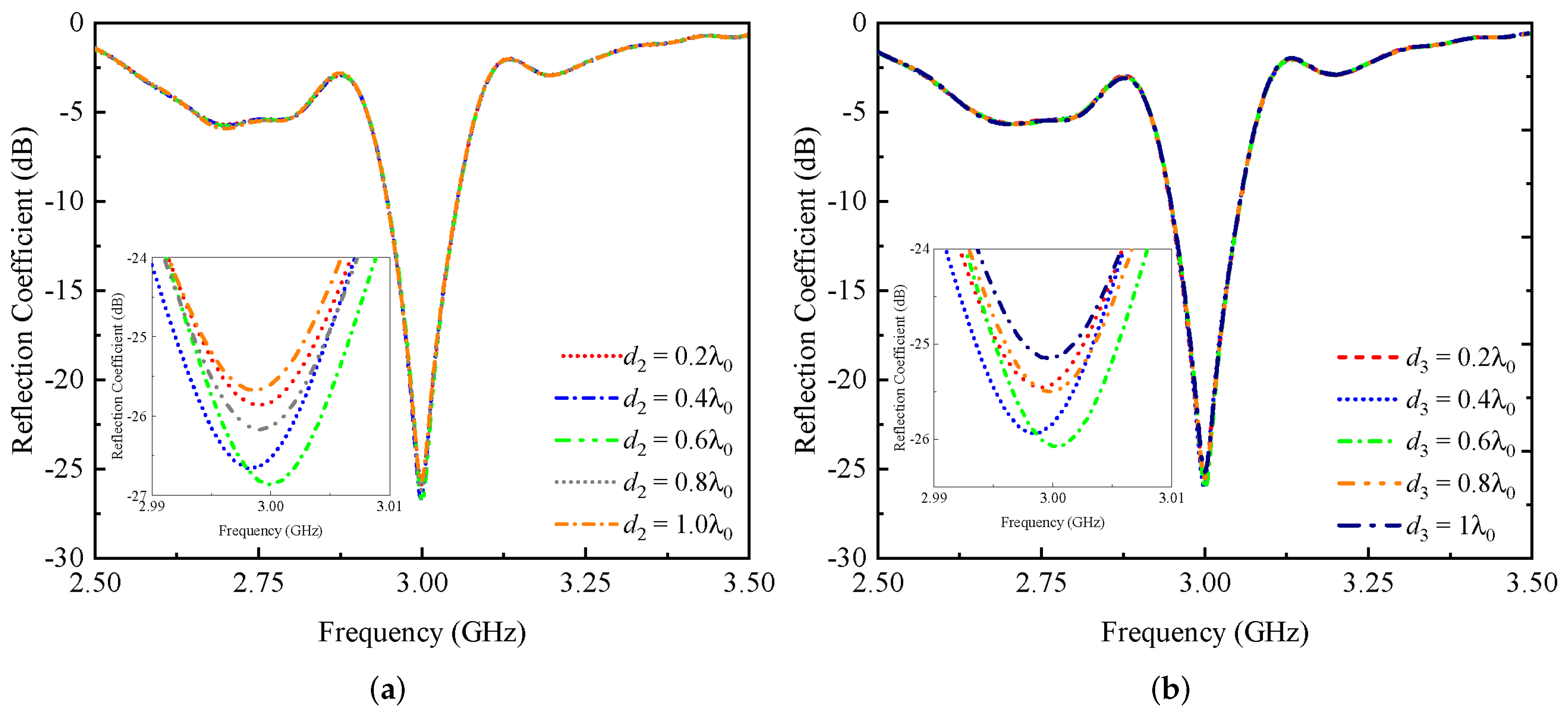
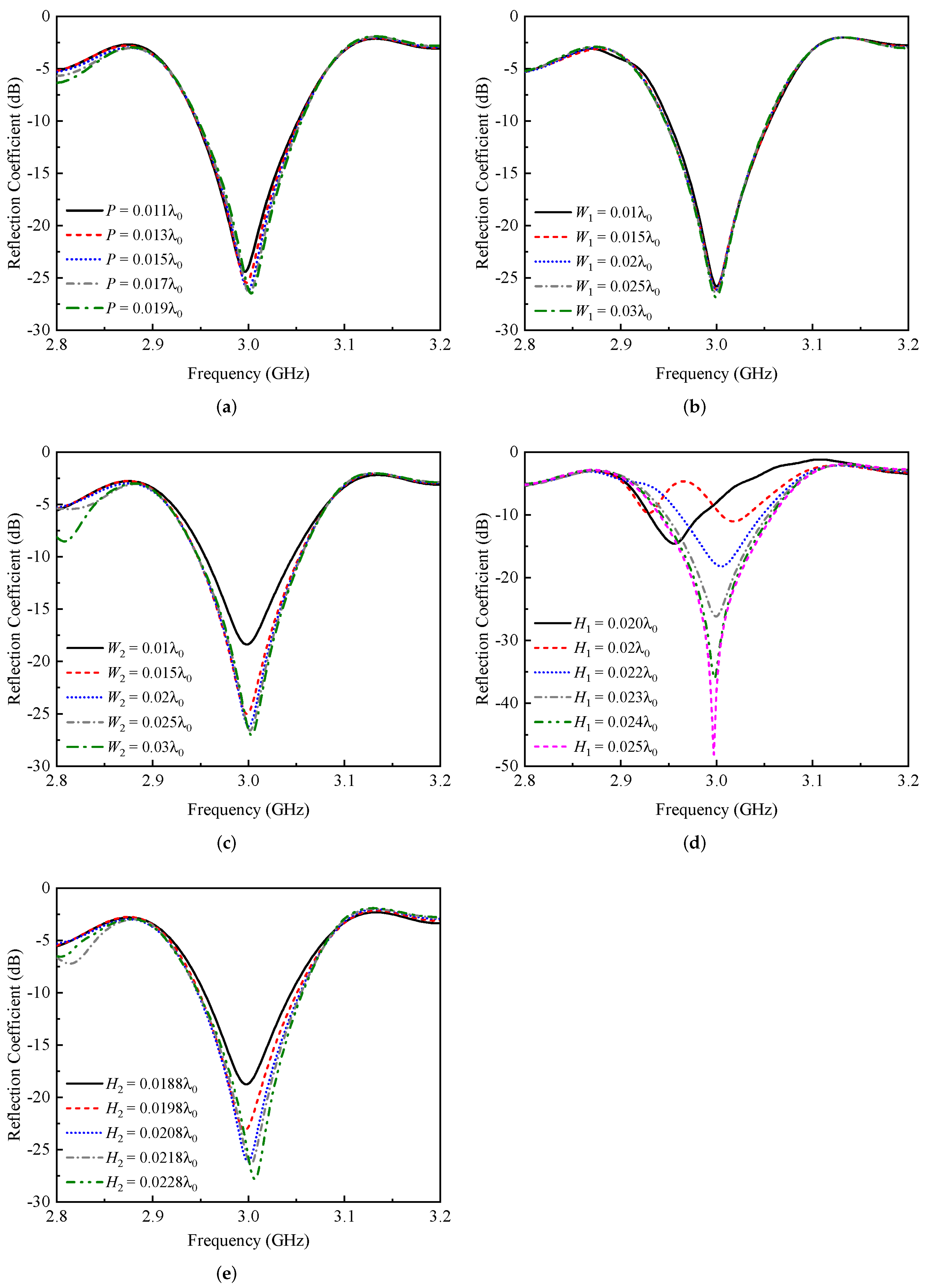
4. Parametric Analysis
A parametric analysis has been performed to observe the effects of different design parameters of SWA with integrated groove. These parameters include: width, position, length, and depth of inside-groove. The variation of these design parameters during fabrication effects the reflection coefficient and far-field characteristics. The effect of groove length is discussed in
Figure 12. By decreasing the length of grooves from the corners, good impedance matching is achieved at
=
= 0.4
.
The effect of groove position is discussed in
Figure 13a. By moving the groove position towards the corners of the waveguide, the resonance frequency shifts towards a higher band. An optimum position was chosen to achieve the better impedance matching at
P = 0.15
. The effects of first and second groove width are illustrated in
Figure 13b,c. The first and second groove widths do not significantly affect the reflection coefficient. A good response of −28 dB is achieved at
=
= 0.04
. The depth of both grooves (
and
) is very critical in controlling the reflection magnitude. By increasing the depth of grooves, a higher reflection coefficient is achieved, as shown in
Figure 13d,e. However, in deeper hollow regions, fabrication difficulties are involved. By keeping the fabrication constrictions, an optimum depth was chosen for both grooves (
= 0.23
and
= 0.208
). The effect of design parameters on the radiation patterns is illustrated in
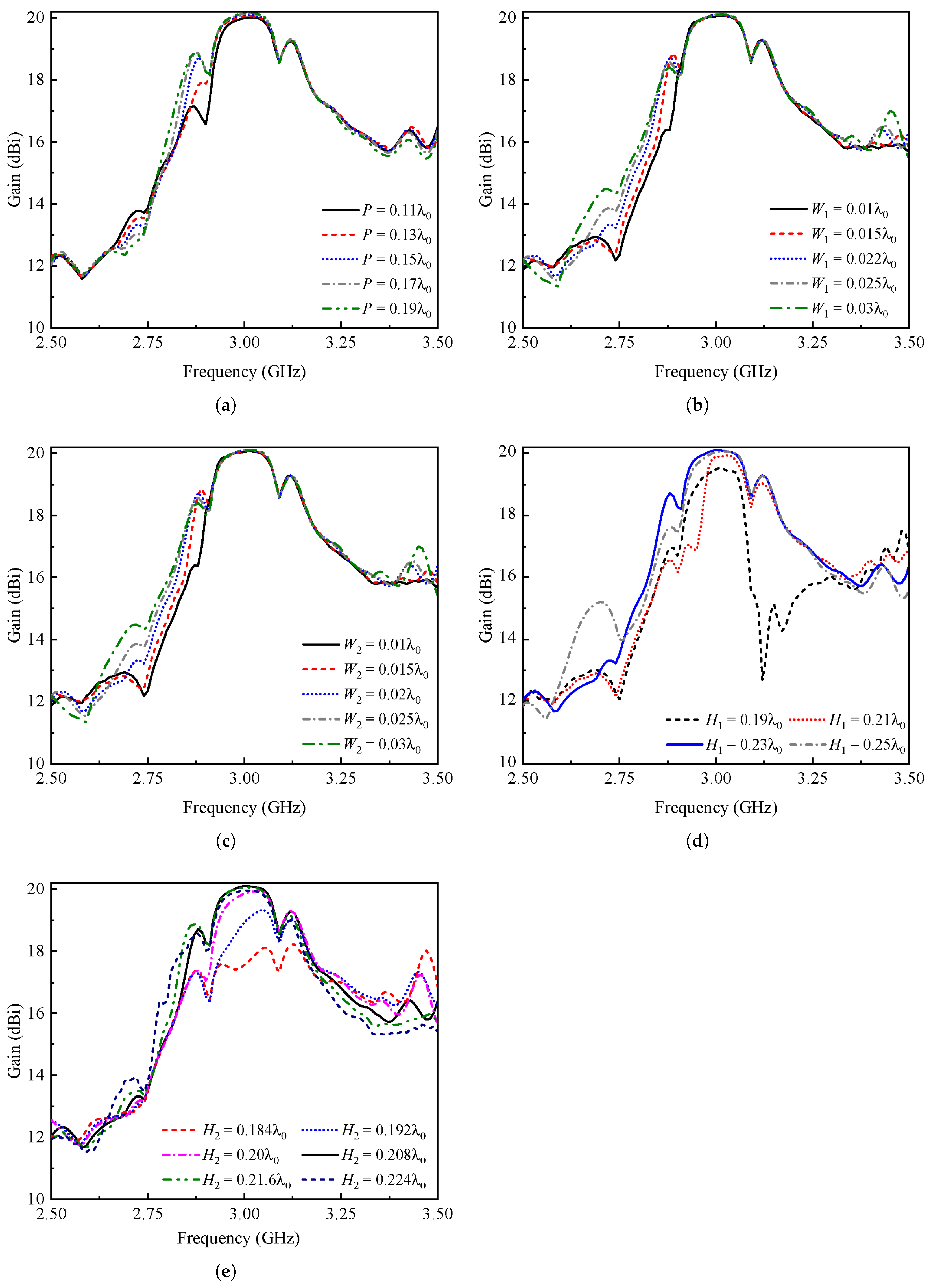
Figure 14. The position of grooves in view of fabrication limitations is chosen, which does not affect the patterns by more than 0.7 dBi (see
Figure 14a). The width of both grooves is also optimized according to the fabrication limitations. The effect of
and
is shown in
Figure 14b,c. It is observed that the width has a minor effect on the gain of SWA. The most important and critical parameter is the depth of both grooves. By increasing the depth of grooves, gain is also increased, as shown in
Figure 14d,e.
5. Experimental Results
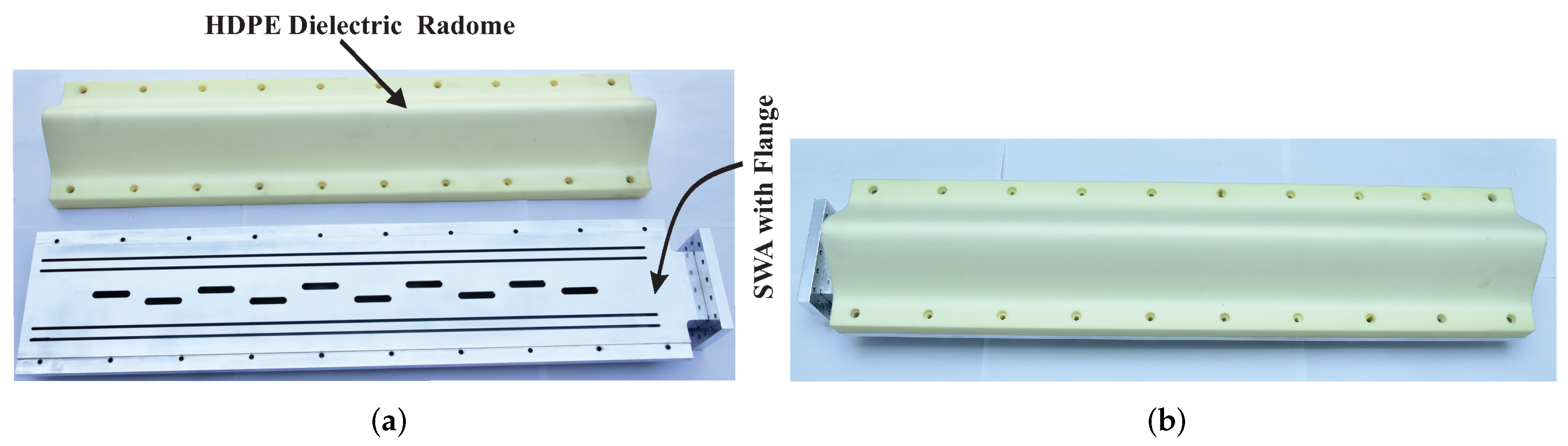
The fabrication process of the high gain SWA system consists of two parts. Firstly, the fabricated SWA prototype is made of aluminium material by using the milling process. The top round-edged radiating slots, along with waveguide walls, are made in a single piece and then coupled and sealed to the bottom SWA plate. The internal surface of the fabricated antenna is mirror finished to reduce the internal ohmic losses and improve the efficiency. Secondly, the Gaussian dielectric radome is made of HDPE material to be compatible for HPM applications and external environmental protection. The SWA and dielectric radome are separately illustrated in
Figure 15a. The full assembly of SWA with HDPE radome is shown in
Figure 15b.
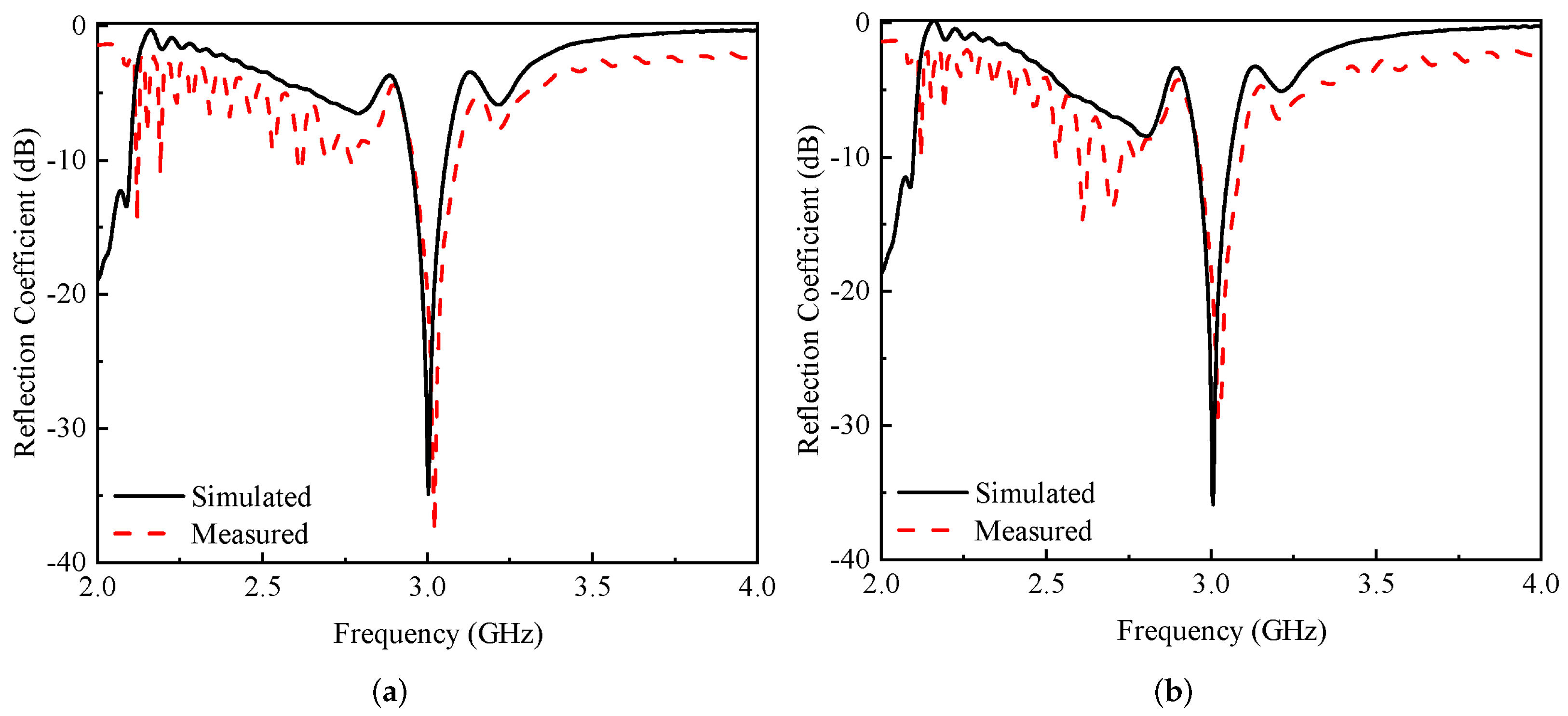
The simulated and measured reflection coefficient of the proposed SWA is depicted in
Figure 16. A measured reflection coefficient of more than −20 dB is achieved at the 3 GHz frequency band without a dielectric radome (see
Figure 16a), while in the presence of a dielectric radome, a reflection coefficient value of −18 dB is achieved, as illustrated in
Figure 16b. The simulated SWA results have good agreement with the measured ones. A little shift in the reflection coefficient is observed due to the fabrication errors and tolerances.
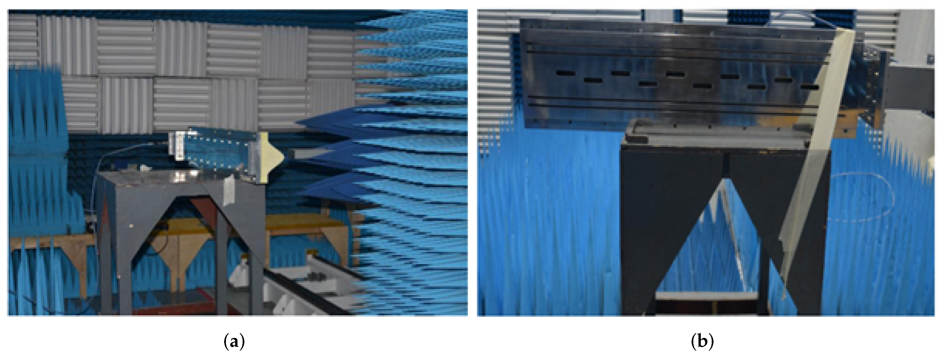
The proposed SWA, with and without dielectric radome, far-field radiation performance is measured in the near-field antenna measurement setup under an anechoic environment as illustrated in
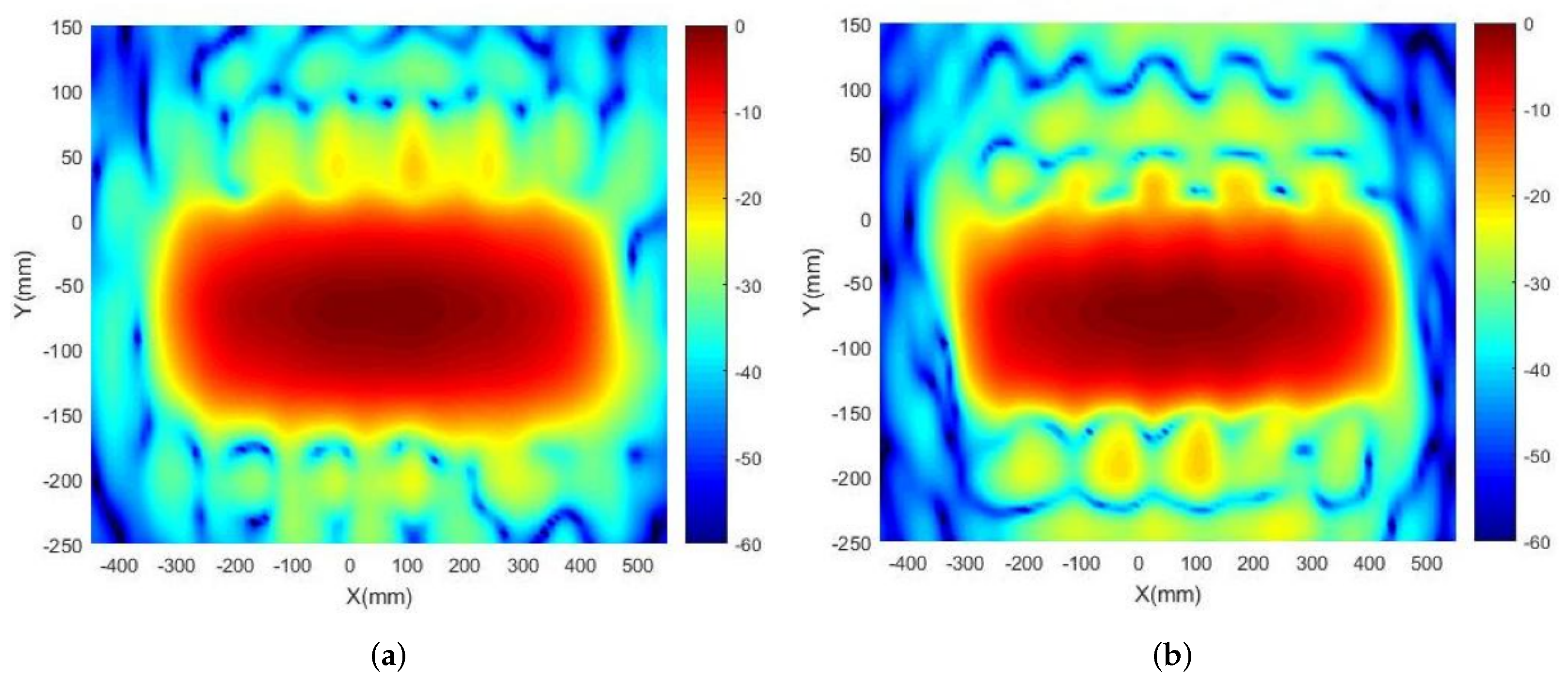
Figure 17. The aperture field distribution with and without dielectric is depicted in
Figure 18. It can be observed that all slots are radiating properly and contribute to far-field radiation characteristics.
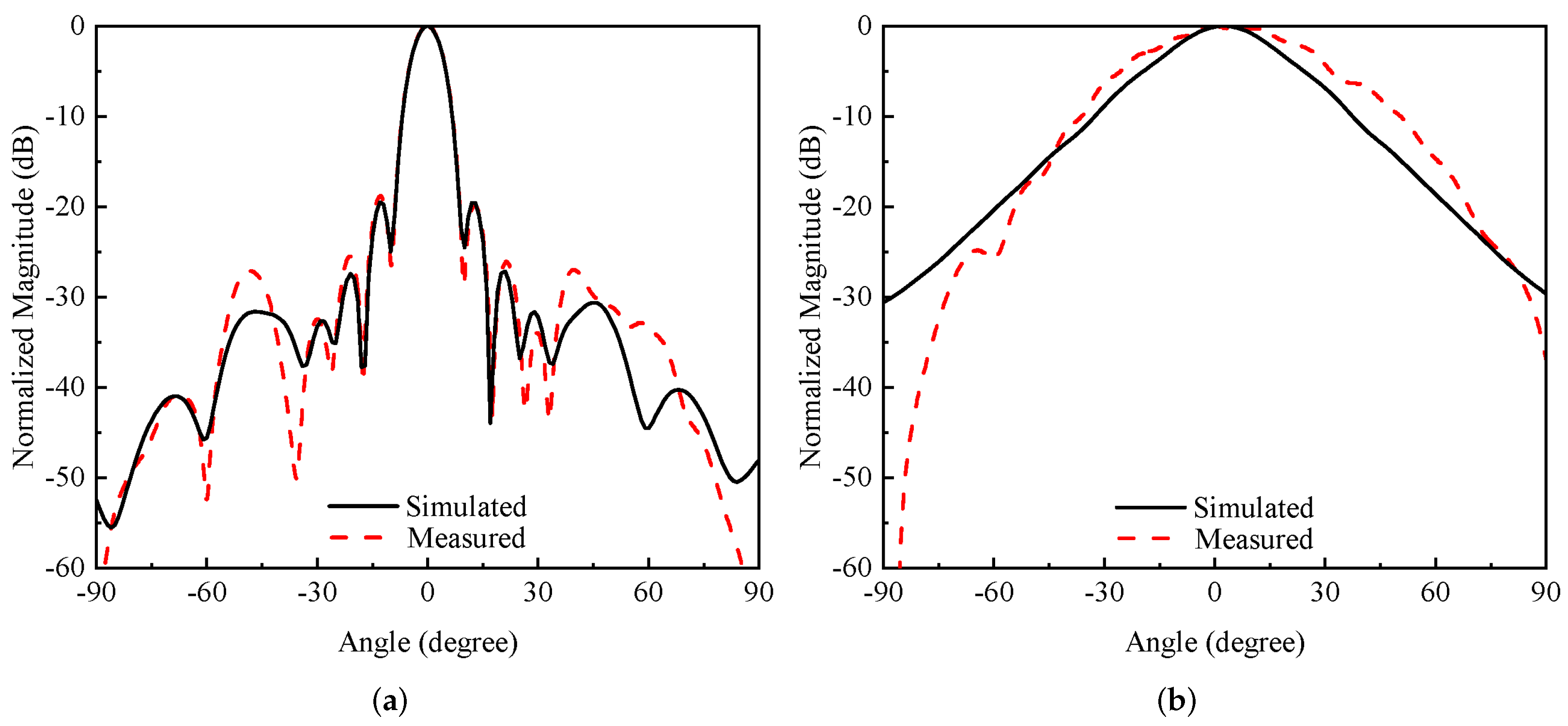
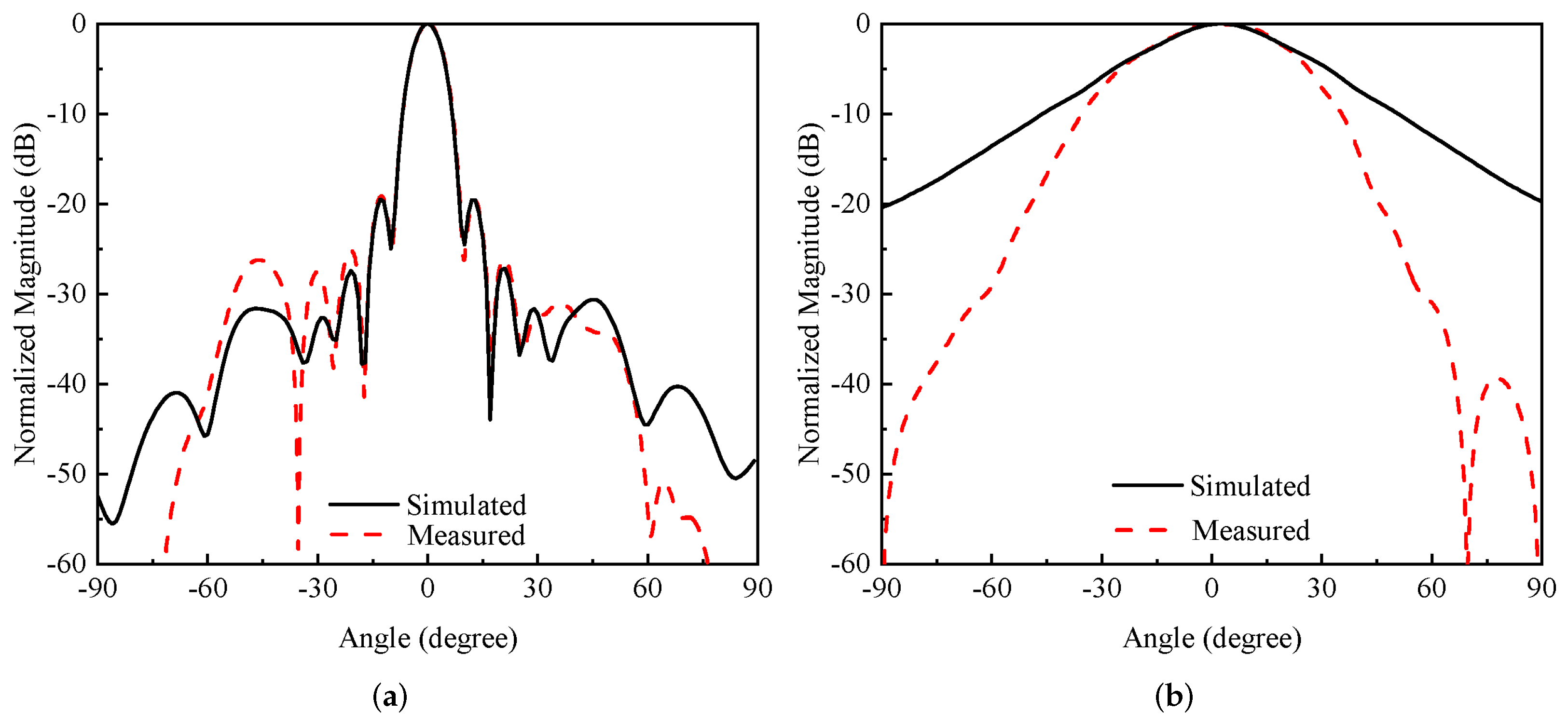
The simulated and measured E- and H-plane radiation characteristics with and without dielectric radome are shown in
Figure 19 and
Figure 20. The radiation patterns in the H-plane are perfectly matched with little distortion in some regions, which is within acceptable limits. However, a significant mismatch in E-plane is observed between simulated and measured patterns due to fabrication errors and measurement setup limitations. A complete simulated and measured result comparison is also given in
Table 6.


 ,
, 


