Review

Modeling Push–Pull Converter for Efficiency Improvement

Faculty of Electrical Engineering, University of Banja Luka, 78000 Banja Luka, Bosnia and Herzegovina
*
Author to whom correspondence should be addressed.
Electronics 2022, 11(17), 2713; https://doi.org/10.3390/electronics11172713
Submission received: 20 June 2022 / Revised: 6 August 2022 / Accepted: 7 August 2022 / Published: 29 August 2022
(This article belongs to the Section Power Electronics)

Abstract

:
In this paper, we model and analyze the power losses of push–pull converters. The proposed model considers conduction and dynamic power losses, as well as transformer and inductor losses. Transformer and inductor models include skin and proximity effects, as well as power losses in the core. Moreover, the model includes the diode recovery time losses. We derived the equations for both continuous and discontinuous current operating modes. All model parameters can be obtained either from the datasheets of the used components or by simple measurement techniques. The model is verified experimentally by measuring the efficiency of the 500 W push–pull converter prototype. Simulations and experimental validation are conducted using the assumption that the converter is used in a permanent magnet (PM) wind turbine generator.

1. Introduction

With the ever-increasing consumption of electrical energy followed by environmental pollution as a result of its production, the renewable power sources gain in popularity [1,2,3]. Due to the variability of the primary energy source, (e.g., wind turbine with variable rotation speed, photovoltaic sources, and fuel cell-based sources), in most cases it is not possible to directly connect the generator to the grid [4]. Power converters are typically used to connect these sources with the grid. In other words, they are used to match the characteristics of the energy source with the requirements of the grid (voltage, frequency, active and reactive power control). This is one of the reasons why power converters have become an inevitable part of any renewable power source of electrical energy [5,6].
It is a common case that the output voltage of a generator in a renewable power source is not high enough, which requires the usage of a DC/DC converter to increase the voltage. Depending on safety standards and/or voltage level requirements, different topologies, namely with or without galvanic isolation, can be employed. A boost converter is often used topology without galvanic isolation [7,8,9,10], while full bridge and push–pull (Figure 1) topologies are selected when galvanic isolation is required or when the ratio between input and output voltage is high enough to bring in some safety concerns [10,11,12,13]. The push–pull converter is simpler from the control standpoint in comparison to full bridge topology. This is because it contains only two switching elements on the primary side.
In renewable power sources, total power from the generator is transferred via a power converter. Therefore, the energy efficiency of the used converter is very important. Modeling power losses is an important step when developing algorithms aimed at improving the efficiency of push–pull converters. In addition to accuracy, a desirable characteristic of every model is to ensure that simulation execution time is as short as possible [14]. Furthermore, it is advantageous if the model parameters for the used components can be obtained from the datasheets or by simple measurement techniques [15,16,17].
To the best of our knowledge, there are no published studies that consider a power losses model of the push–pull converter. Conversely, there are papers that provide power loss models for the boost (without galvanic isolation) and the full bridge (with galvanic isolation) converters.
There are many models reported in the literature that are used to evaluate the efficiency of the converter. However, these models typically focus on specific application conditions. For example, in [18], the authors considered only conduction losses of the boost converter, while in [19] the authors provided a model in continuous current mode (CCM). In [15], the model is extended in a way that significant sources of dynamic losses are provided, whereas the modeling inductor core and winding losses due to skin and proximity effects is missing. The same applies to the power losses models of the full bridge converter. In [20], a power losses model for the full bridge converter under light load conditions is given. This model, however, does not include power losses due to the proximity effect in the transformer and the output inductor wires. Likewise, the models presented in [21,22] do not include power losses caused by the skin and proximity effects, and the model derived in [21] is applicable only for the CCM operating mode of the converter.
Many algorithms aiming at optimizing efficiency are based on the variable switching frequency. When developing any of these algorithms, accurate modeling of dynamic losses of the converter, both in CCM and discontinuous (DCM) current modes, is a critical task. The existing models of the used components, which are available in the SPICE simulator, are sufficiently accurate for modeling the converter operation. However, the inductor model in this tool does not consider winding losses caused by skin and proximity effects. More importantly, the SPICE simulations are typically time-consuming and may introduce convergence issues [14].
In this paper, we derived an analytical power losses model for a push–pull converter that is suitable for discovering the optimal efficiency operating point of the converter subjected to its components and the switching frequency. The derived model is applicable for both operating modes of the converter (CCM and DCM). We provide analytical expressions for conduction and dynamic losses, including losses in transformer, inductor, and switching losses due to diode recovery time. Moreover, transformer and inductor winding power losses due to skin and proximity effects are also considered in the paper. The power losses equations for the snubber circuit protecting the switching transistors are provided, as well as the equations for the snubber circuit in the rectifier. Finally, the equations for power losses in MOSFET are given. In Table 1, we summarize point by point comparison between the proposed model and the existing models reported in the literature. The comparison is based on several power loss sources and certain characteristics of the provided models.
We verified the model using simulative assessment and experimental measurements on push–pull converter that is used in a wind turbine with a permanent magnet generator. The model verification is conducted in the function of switching frequency and the load of the converter.
The paper is organized as follows. In Section 2, we derived mathematical equations that describe the power loss model of the push–pull converter. Additionally, in Section 2 we provide the details about the hardware prototype that we used for the model verification in Section 3. A short analysis of the power losses for the converter is given in Section 4. Finally, we conclude the paper by summarizing and discussing the results in Section 5.

2. Materials and Methods

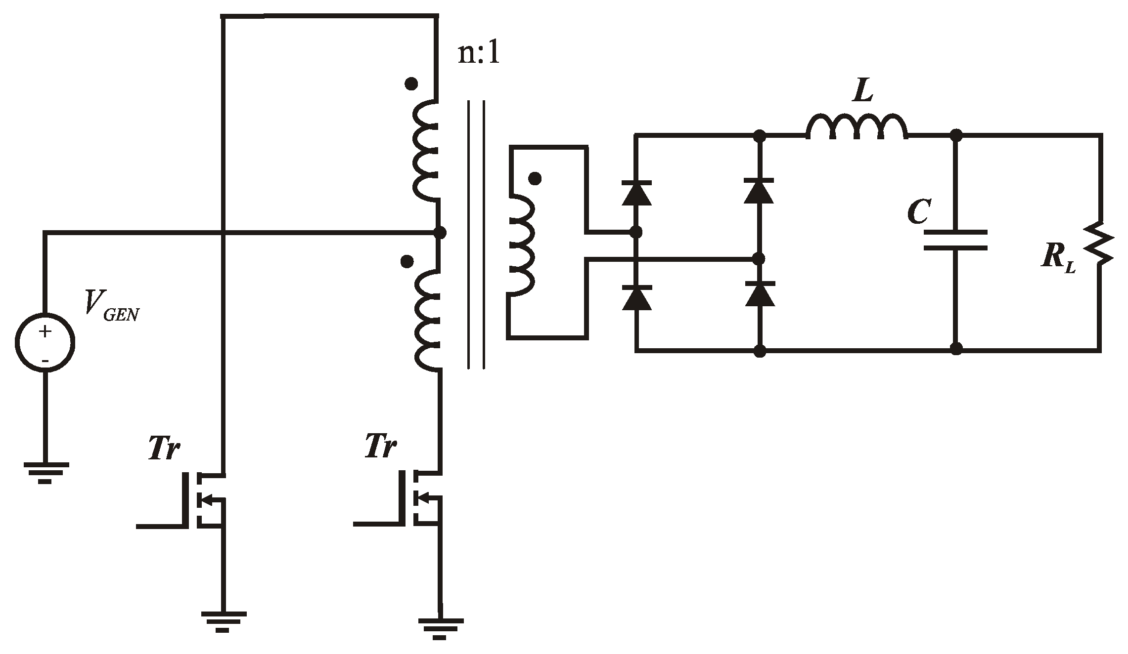
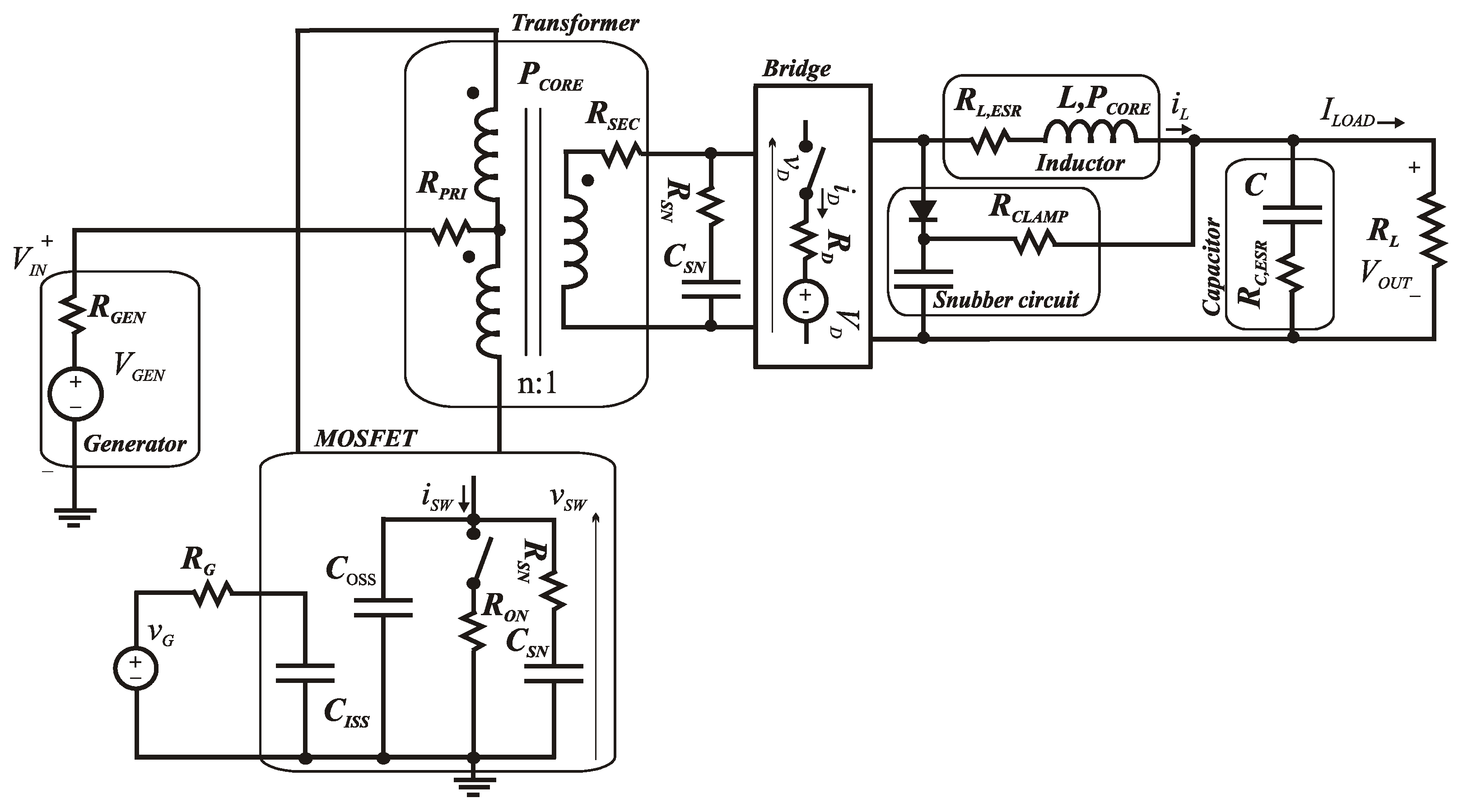
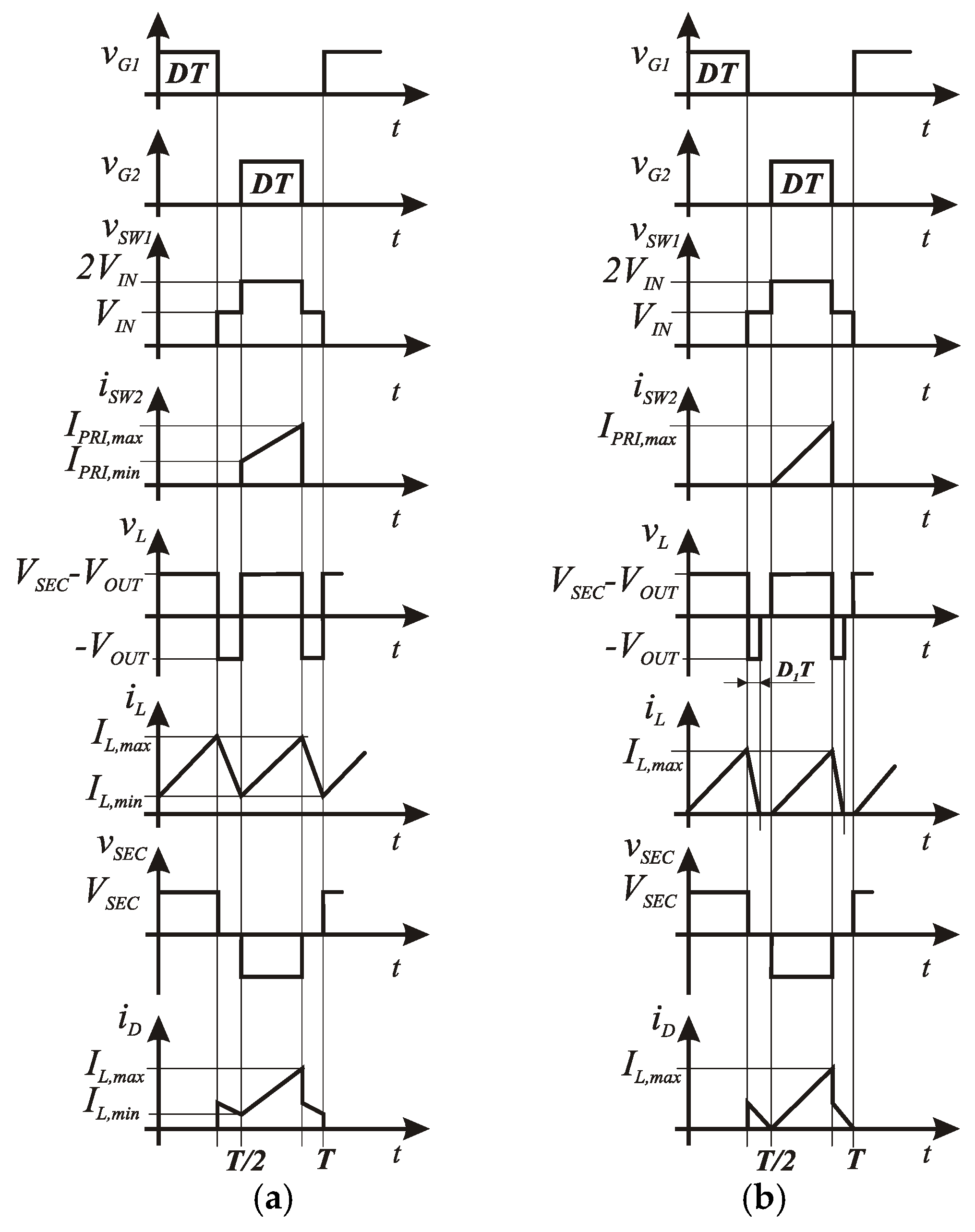
2.1. Power Losses of Push–Pull Converter

The overall converter efficiency is defined as:
η = P O U T P I N × 100 % = P I N P L O S S P I N × 100 % ,
where PIN stands for input power, POUT represents output power, and PLOSS covers total power losses in the converter. Clearly, the efficiency can be easily derived from (1) if we know how to calculate total power losses.
As given in [23], the total power losses PLOSS can be expressed as:
P L O S S = P C O N D + P F I X E D + W T O T f s w ,
where: PCOND—conduction losses, PFIXED—fixed losses, WTOT—total energy consumed during one period. Average dynamic power losses can be represented as PDYN = WTOT·fsw. Clearly, the dynamic losses directly depend on switching frequency fsw. On the other end, controller power supply current and leakage currents contribute to fixed losses. They are negligible in comparison to conduction and dynamic losses and, therefore, can be excluded from further analysis.
Equivalent circuit of the push–pull converter, including the parasitic elements, is depicted in Figure 2. When MOSFET is used as a switching element, it can be modeled with RON (when turned on). The model also includes the transistor input capacitance CISS. Diode (forward-biased) is modeled using constant voltage source VD and resistance RD.
The equivalent circuit also includes power losses on RC,ESR (equivalent series resistance of the output filter capacitance). Similarly, inductor equivalent series resistance (RL,ESR) accounts for its conduction losses. In addition, we consider inductor core power losses. Finally, the supply circuit is modeled as a series of resistance RGEN and voltage generators, where RGEN represents converter supply circuit losses. In [23], an analytical expression is given for RGEN for the case when the supply circuit consists of AC generator and single-phase or three-phase rectifier.
Conduction losses of push–pull converter can be calculated using the following equation:
P C O N D = P L , C O N D + P T R , C O N D + 2 R O N I S W , e f f 2 + 4 R D I D , e f f 2 + 4 V D I D , a v g + R C , E S R I C , e f f 2 + R G E N I I N , e f f 2 + P C L A M P ,
where ISW,eff, ID,eff, IC,eff, IIN,eff represent effective values of currents through switch, diode, output capacitor and converter input, respectively. ID,avg is average diode current. PL,COND and PTR,COND are conduction losses in inductor and transformer windings, respectively. PCLAMP is power dissipation of the limiting circuit of the rectifier output.
The currents through inductor and transformer have periodic non-sinusoidal waveform. In that regard, we can separately analyze conduction losses in the windings caused by DC and AC currents [24]. For both CCM and DCM operating modes, it can be assumed that the amplitude of the fundamental harmonic prevails when compared with other harmonics. Therefore, we can safely confine the winding conduction losses caused by AC inductor current to power losses of the fundamental harmonic. Given all above, overall conduction losses are approximated as
P L , C O N D = R L , E S R , D C I L , A V G 2 + R L , E S R , A C I 1 L , E F F 2 .
Here, RL,ESRL,DC represents inductor equivalent serial resistance for DC current. The second term in (4) accounts for power losses in the winding due to the skin and proximity effects, where RL,ESR,AC denotes inductor resistance for the AC current I1L,EFF at the switching frequency.
By using the equation for effective value of periodic non-sinusoidal signals, we approximate the inductor effective current for the fundamental harmonic as
I 1 L , E F F I L , E F F 2 I L , A V G 2 .
Furthermore, RL,ESR,AC is given by the following Equation [25]:
R L , E S R , A C R L , E S R , A C | f s w = i = 1 m ξ R D C , m 2 × [ sinh ( ξ ) + sin ( ξ ) cosh ( ξ ) cos ( ξ ) + ( 2 m 1 ) 2 sinh ( ξ ) sin ( ξ ) cosh ( ξ ) + cos ( ξ ) ] ,
where m stands for number of layers of the inductor winding and RDC,m represents resistance of the mth layer for DC current
R D C , m = ρ N m l m , t u r n A W .
In the equation above, ρ is resistivity of the wire, Nm number of turns in the mth layer, lm,turn one turn wire length, and AW is the wire cross-sectional area. Moreover, ξ from (6) is characterized as
ξ = d π 2 δ ,
where d represents the diameter of the wire and δ stands for skin depth, which can be calculated as
δ = ρ π f s w μ ,
where μ is wire permeability.
The power dissipation of the limiting circuit of the rectifier output can be determined by:
P C L A M P = ( V S E C V O U T ) 2 R C L A M P ,
where VSEC is voltage amplitude on transformer’s secondary winding.
Total dynamic power losses of push–pull converter are calculated as:
P D Y N = P I S S + P S W + P B R I D G E + P L , C O R E + P T R , C O R E + P S W , S N U B + P S E C , S N U B ,
where: PISS is power loss in transistor gate, PSW is power loss during switching, PBRIDGE is power loss in rectifier, PL,CORE is dynamic power loss in inductor core, PTR,CORE is dynamic power loss in transformer core, PSW,SNUB is power loss in snubber circuit of the switch, and PSEC,SNUB is power loss in snubber circuit of the transformer’s secondary winding. We note here that, in the case of push–pull converter, if snubber circuit is used on the transformer’s secondary winding, then limiting circuit is not used and vice versa.
Switch gate power losses are expressed as [26]:
P I S S = 2 Q G V C G f s w .
where QG is total charge in the gate and VCG is supply voltage of gate control circuit.
In the case of MOSFET, the power losses come up when the switches transit between the states and is given by
P S W | M O S F E T = 2 k ( t v f I L , M A X + t v r I L , M I N ) V O U T f s w ,
where tvr and tvf are rising and falling time of the output voltage, respectively. Factor k is between 1/6 and 1/2 [27]. Rising and falling times can be calculated using the equations from [16]:
t v f = Q G ( S W ) / I D R I V E R ( L H ) ,
t v r = Q G ( S W ) / I D R I V E R ( H L ) .
Here, QG (SW) represents gate charge at the switching point, which can be expressed with the following equation:
Q G ( S W ) = Q G D + Q G S 2 ,
The MOSFET gate currents, when transistor turns on and off, are, respectively, given by
I D R I V E R ( L H ) = V D D V S P , O N R D R I V E R ( P U L L U P ) + R G ,
I D R I V E R ( H L ) = V S P , O F F R D R I V E R ( P U L L D O W N ) + R G ,
where VSP,ON and VSP,OFF are voltages at the switching points. The values of these voltages can be retrieved from the gate charge diagram from the MOSFET specifications. Alternatively, they can be calculated approximately with equations:
V S P , O N V G + I L , M I N g m ,
V S P , O F F V G + I L , M A X g m .
Here, VG represents gate threshold voltage, and gm stands for MOSFET transconductance.
Normally, dynamic losses contain power losses caused by the discharging process of the switching element (MOSFET) output capacitance COSS. However, the authors in [17] proved that they are already expressed in (13).
Dynamic power losses in rectifier can be calculated as:
P B R I D G E = V S E C ( I L , M I N t r r + 4 Q r f s w ) .
where: VSEC-secondary voltage, trr-diode recovery time, Qr-pn junction accumulated charge. The losses in (21) are present only when the converter operates in CCM. Given that the diode current is zero when transistor turns on, we can conclude that these losses are zero in DCM.
The losses in inductor and transformer cores originate from hysteresis and eddy currents. According to [28,29], we can use Steinmetz’ equation to accurately calculate the core losses
P C O R E = k f s w α Δ B β V C O R E ,
where VCORE represents volume of the inductor core, k, α, and β are coefficients of the core material (retrieved from the specifications), and ΔB stands for the maximum induction in the core.
Induction change in the transformer’s core is given by:
Δ B = V I N D T 2 N P A ,
where NP is number of turns in primary winding.
Induction change in the core of the output inductor is determined with:
Δ B = Δ i L L 2 N A ,
while push–pull converter current change (ΔiL) is calculated using the equation:
Δ i L = V O U T ( 1 / 2 D ) L f s w .
When snubber circuits connected in parallel with the switches are used, dissipated power can be determined using:
P S W , S N U B = 2 V I N 2 C S N f s w ,
where CSN is capacitance of the snubber circuit.
Power losses due to the snubber circuit in transformer’s secondary winding are calculated using:
P S E C , S N U B = V S E C 2 C S N f s w .
The waveforms of characteristic voltages and currents for the push–pull converter (both operating modes) are illustrated in Figure 3.
Effective inductor current IL,eff, in CCM operating mode of the converter, can be derived from the waveform shown in Figure 3a:
I L , e f f = I L , max 2 2 D ( I L , max 2 I L , min 2 ) Δ I L I L , max + Δ I L 2 D ( I L , max + I L , min ) + Δ I L 2 3 .
Maximum and minimum values of the inductor current are determined with:
I L , max = I L , a v g + Δ i L 2 ,
I L , min = I L , a v g Δ i L 2 ,
where IL,avg = ILOAD. Effective currents through the secondary winding and switch are expressed as:
I S E C , e f f = 2 D ( I L , min 2 + Δ I L I L , min + Δ I L 2 3 ) ,
I S W , e f f = D ( I P R I , min 2 + ( I P R I , max I P R I , min ) I P R I , min + ( I P R I , max I P R I , min ) 2 3 ) .
By knowing the transformer’s turns ratio n, the maximum (IPRI,max) and minimum (IPRI,min) currents are given as follows:
I P R I , max = I L , max n ,
I P R I , min = I L , min n .
Effective currents through the primary winding and the diode can be determined with:
I P R I , e f f = 2 I T R , e f f ,
I D , e f f = I S E C , e f f 2 .
The average current values through primary winding, secondary winding, and diode, in CCM operating mode, are calculated as:
I P R I , a v g = D ( I P R I , max + I P R I , min ) ,
I S E C , a v g = n I P R I , a v g ,
I D , a v g = I S E C , a v g 2 .
In DCM operating mode of the converter, the maximum inductor current is
I L , max = ( V I / n V O ) f s w L .
Minimum inductor current and, therefore, the minimum current in the primary winding are equal to zero in this case.
Effective and average current values, when the converter operates in DCM mode, can be derived from the waveforms shown in Figure 3b. For effective current of the inductor (IL,eff) we obtain
I L , e f f = I L , max 1 3 ( 2 D + D 1 )
whereby D1 is defined as
D 1 = ( V I n V O 1 ) D .
Effective currents through the switch and the secondary winding are given by
I S W , e f f = I P R I , max 1 3 D ,
I S E C , e f f = I L , max 2 3 D ,
while the effective currents through the primary winding and the diode are calculated as
I P R I , e f f = 2 I T R , e f f ,
I D , e f f = I S E C , e f f 2 .
The average value of the primary current in DCM operating mode is determined with
I P R I , a v g = D I P R I , max ,
while (38) and (39) can be used to obtain the average currents through the secondary winding and the diode, respectively.

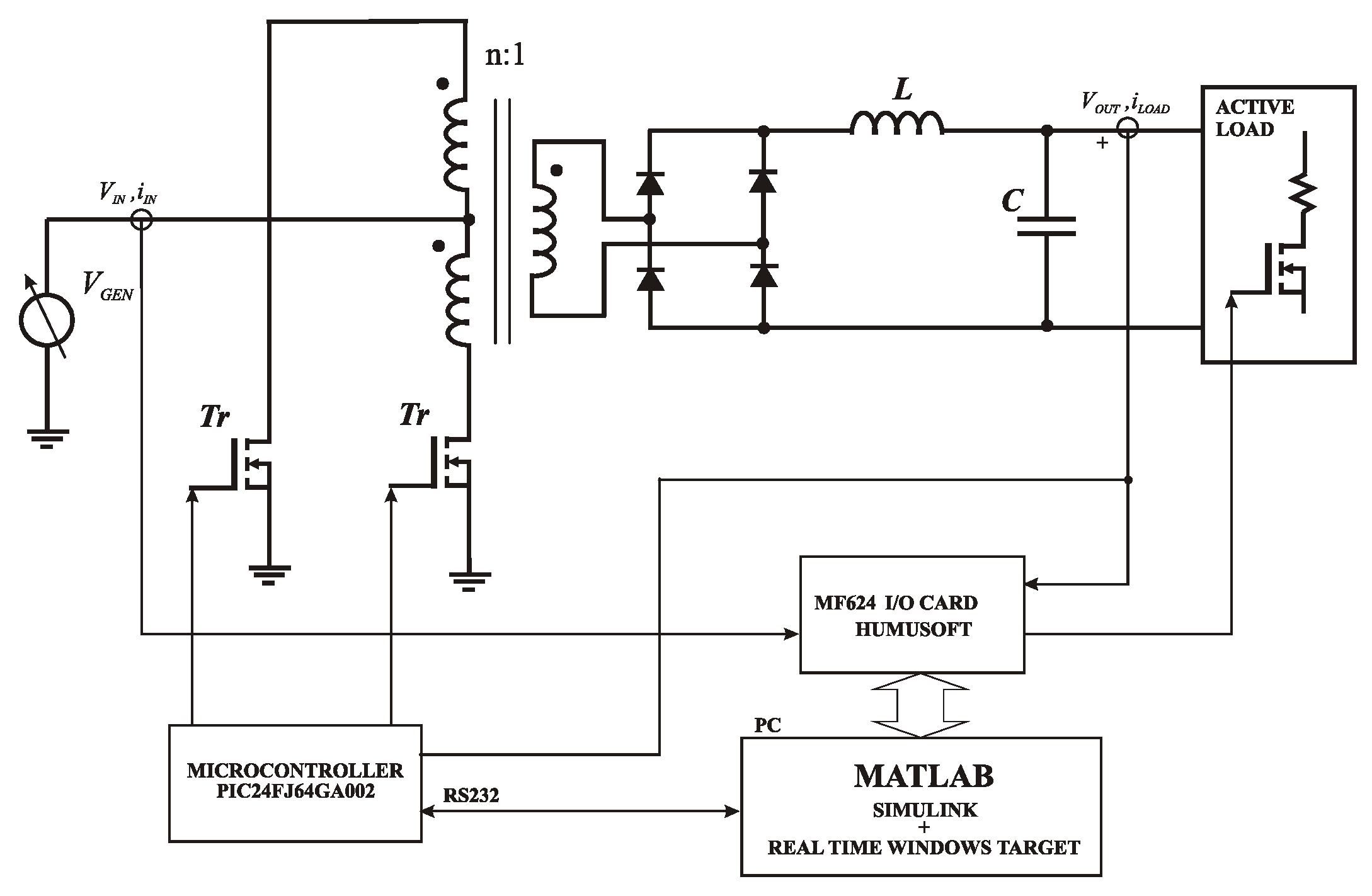
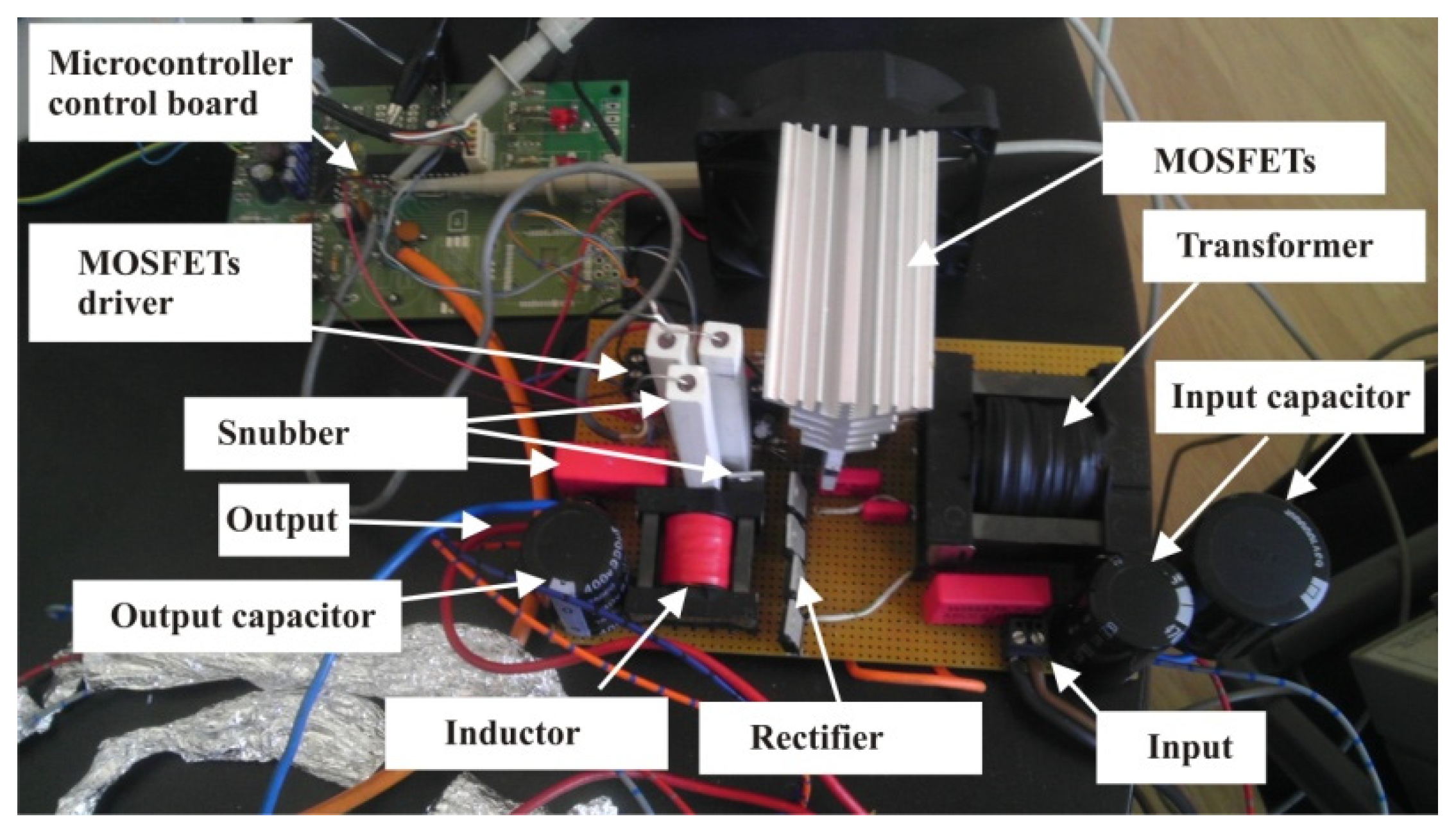
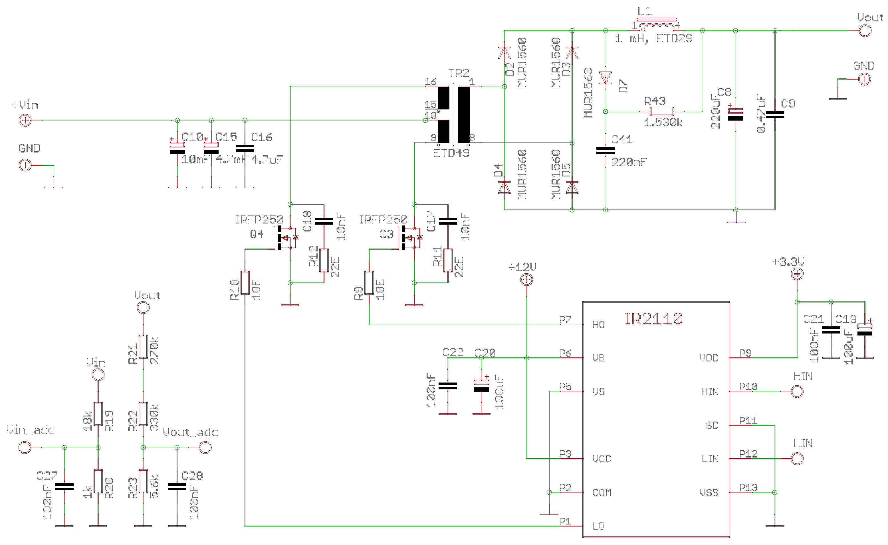
2.2. Experimental Setup of Push–Pull Converter

In Figure 4, a block diagram of experimental setup for measuring parameters of push–pull converter is shown. Specifications of the converter are as follows:
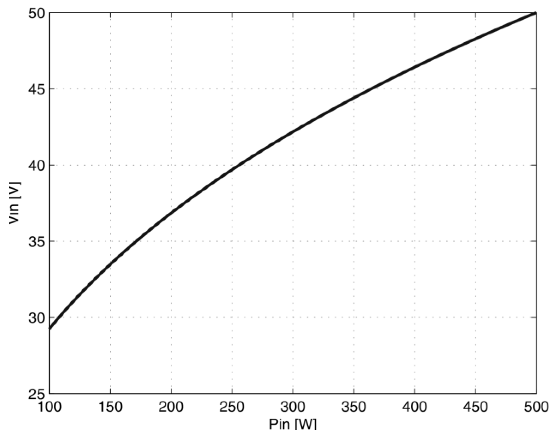
  • DC input voltage VIN = 30–58 V;
  • DC output voltage VOUT = 300 V (0–100% load);
  • maximum output power POUT = 500 W;
  • switching frequency fsw = 10–100 kHz.
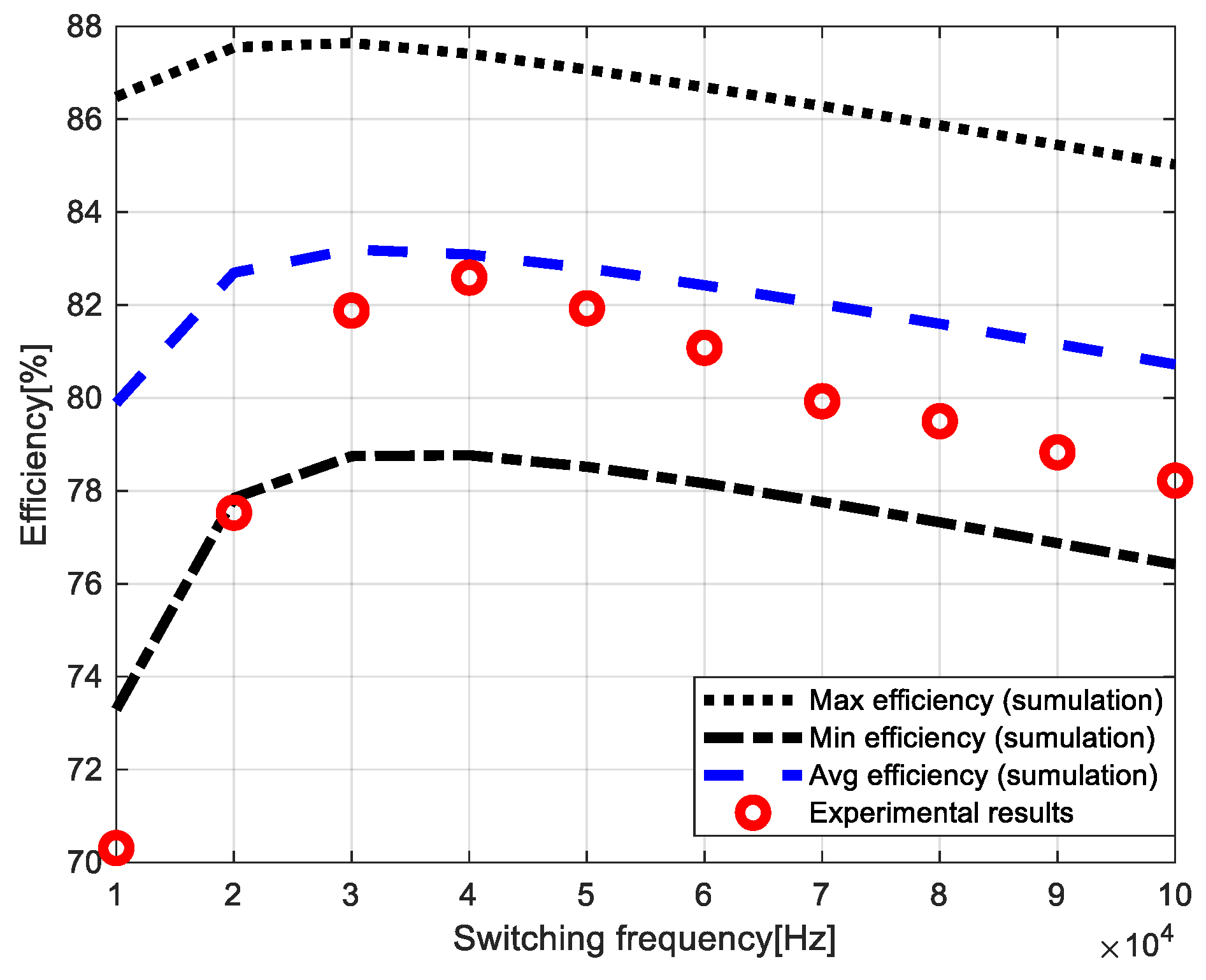
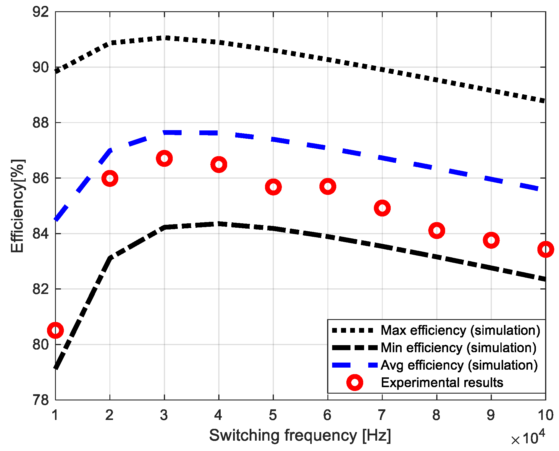
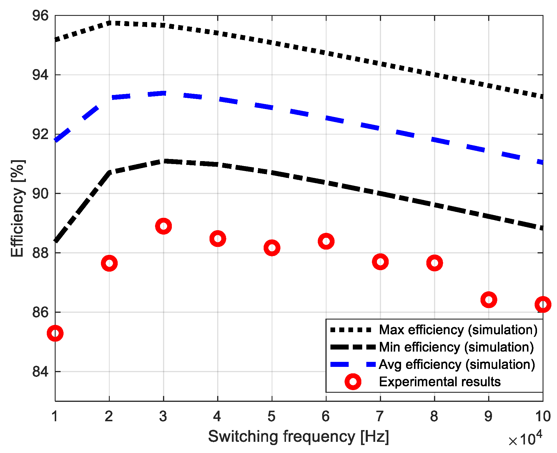
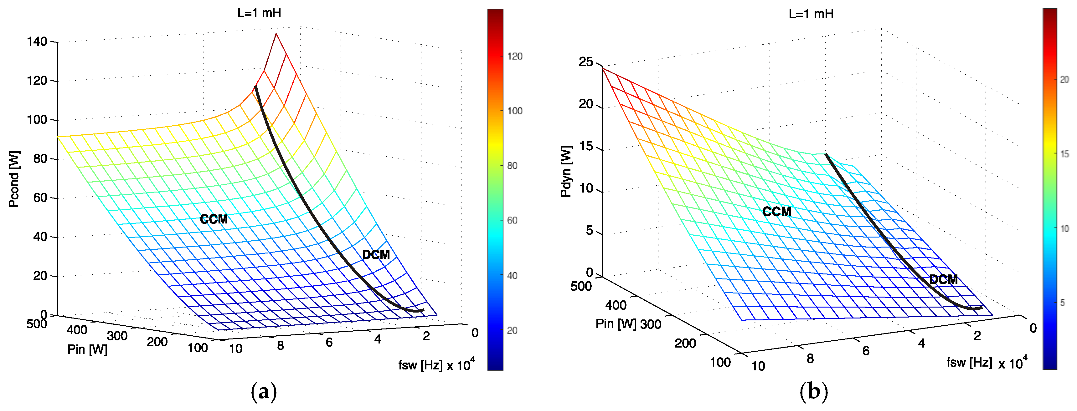
The converter components were selected to meet the specification listed above.
The transformer’s core is made of ferrite material N67 with ETD49 shape and shape of the output inductor’s core is ETD29 with air gap of 1 mm. The primary winding of the transformer contains 8 turns (Np/2) of AWG 13 wire, while the secondary winding consists of 84 turns of AWG 17 wire. The inductor winding contains 79 turns of AWG 21 wire, which makes total wire length of 2.86 m and inductance of about 1 mH. Capacitance of the filter capacitor at the input of the converter is around 10 mF with the equivalent serial resistance of around 0.015 Ω. Output filter capacitor of the push–pull converter has capacitance of 220 µF with the equivalent serial resistance of around 0.25 Ω. We used MOSFET IRFP250 as a switch, and bridge rectifier was realized with MUR1560 diodes. A controller part of the push–pull converter is implemented using PIC24FJ64GA002 microcontroller. For measuring efficiency of the converter, HUMUSOFT MF624 acquisition card featuring MATLAB Simulink with Real-Time Windows Target was used. Power measurement error is 1%. Resistor, 75 Ω, and MOSFET were used to simulate the variable load of the converter. The wind turbine with PM generator is emulated using HP 6674 A DC power supply. The generator resistance (Rgen) is not modeled and, therefore, it is not considered in simulation and experimental results.
Figure 5 shows electrical schematic of the push–pull converter. Integrated circuit IR2110 was used as a driving circuit for the transistors. To protect diodes in bridge rectifier from voltage spikes, we used a voltage limiter made of diode D7, capacitor C41, and resistor R43. Hardware prototype of the push–pull converter is shown in Figure 6.

3. Results

When validating the power loss model of the converter, we preserved the relationship between the input voltage and the input power as the converter was a part of a wind turbine with a PM generator, whose characteristic is shown in Figure 7. The switching frequency was changed during an experiment in the range from 10 to 100 kHz with a 10 kHz increment.
Efficiency of the converter, as a function of switching frequency, is depicted in Figure 8, Figure 9 and Figure 10. Here, we note that the figures show the efficiency for different values of input power.
To account for deviations that emerge during fabrication process of the components, manufacturers typically provide broader range for the parameters in the technical specifications. One such example is drain–source resistance of the MOSFET (RDS), which is used to model transistor on state. In datasheet, two values are usually given: typical (RDS,TYP) and maximum (RDS,MAX) value. Given the above, we performed simulations for two distinct scenarios: best case, (e.g., using RDS,TYP) and worst case, (e.g., using RDS,MAX) with respect to the converter efficiency.
The red circles in Figure 8, Figure 9 and Figure 10 present experimental results, while black curves designate maximum and minimum values of the converter efficiency obtained from the simulation model. The blue curve represents the average efficiency obtained using simulations. The average value can be used as a reference for comparing the simulation and experimental results.
Figure 8 shows the simulation and experimental results for 500 W input power. Clearly, the maximum efficiency is achieved at the switching frequency of around 40 kHz. By decreasing the input power, the point of maximum efficiency traverses towards the lower switching frequencies (Figure 9).
From Figure 8, Figure 9 and Figure 10, we can see that discrepancies between experimental and simulation results do not exceed 7%. The largest deviation was observed at the lower input power of the converter (Figure 10). Moreover, the difference between experimental and simulation results is more noticeable at lower switching frequencies (Figure 8). For converter analysis, from the point of determining the optimal operating conditions of the converter to achieve maximum efficiency, the qualitative characteristics of the model are more important than its quantitative analysis. In other words, efficiency peak points in simulation results should match the ones obtained experimentally, which is clearly the case for the proposed model.

4. Discussion

Figure 11 illustrate conduction and dynamic losses as a function of switching frequency and input power of the converter obtained by simulations. The solid black line in the figures designates the borderline between the continuous and discontinuous operating modes. When switching frequency is decreased, the changes of the currents through the converter elements rise. This increases effective currents, which leads to an exponential rise in conduction losses (Figure 11a). From Figure 11b, we can see that dynamic losses are proportional to the switching frequency. When transitioning from CCM to DCM, a part of losses emerges in the switch when it is turned on (see Equation (13) or (21)), which makes refraction the characteristic of dynamic losses (Figure 11b). Due to the described decrease in dynamic losses near the boundary between CCM and DCM, it can be expected that push–pull converter will operate with optimal efficiency in this region.
Table 2 summarizes conduction, dynamic, and total losses obtained using simulations for a given input power of the converter and switching frequencies.
Percentages show a share of the given power loss in total losses. Finally, Table 1 also gives average efficiency obtained simulatively and experimentally, along with their absolute difference.
Table 3 and Table 4 show the distribution of conduction and dynamic power losses, respectively, across the components of the push–pull converter for 300 W input power obtained using simulations.
When a DC/DC converter is designed, switching frequency is typically selected to be as high as possible to reduce the size of reactive components. Table 5 provides energy efficiency obtained experimentally for the converter operating at the maximum switching frequency of 100 kHz (η100k) and the maximum measured energy efficiency (ηopt). Additionally, we calculated and presented the total power losses of the converter. On the other end, based on Figure 8, Figure 9 and Figure 10, the maximum efficiency is obtained at lower frequencies. Table 5 also shows improvement in terms of power losses for the case when the converter operates using the optimal switching frequency comparing to the case when the maximum switching frequency is used. Obviously, it should be kept in mind that one must not arbitrarily decrease the switching frequency as it may compromise the designed working conditions.

5. Conclusions

A more accurate power loss model is required when developing control algorithms aimed at improving the efficiency of the converter. How difficult is to obtain the parameters of the model is equally important. All parameters of the presented model are obtained either from the technical specifications of the components or acquired by using simple measurements. The model enables fast simulation with sufficient accuracy for both CCM and DCM.
The proposed model is validated experimentally on a push–pull converter prototype. For both CCM and DCM operating modes, the simulation results diverge from experimental measurements with a maximum deviation of 6.8%.
As reported in the previous section, both experimental and simulation results clearly suggest that the energy efficiency of the converter can be improved by adjusting the switching frequency. Near the DCM region, we observed an increase in the changes of the currents through the elements, which further increases their effective values, and thereby conduction losses. Additionally, AC components of transformer and inductor currents contribute to an increase in the power losses in the winding caused by the skin and proximity effects. On the other end, when the operating point of the push–pull converter transits from continuous to discontinuous operating mode, the minimum current is zero. As an effect, the dynamic power losses caused by diode recovery time and transistor turn-on hard switching also become zero. This effectively refracts the characteristic of the dynamic power losses when it transitions from CCM to DCM. In summary, given the converter elements, we can expect that the maximum efficiency of the push–pull converter is placed near the boundary between continuous and discontinuous operating modes. Therefore, we advocate that the proposed model can be exploited when designing the push–pull converter with optimal elements and for estimating its maximum efficiency operating point.
In future work, we will further improve the provided model by considering the influence of temperature on the parameters of the used components. Furthermore, using the presented power losses model, we plan to determine the optimal operating mode with respect to the energy efficiency of the push–pull converter, and propose a suitable control algorithm for maintaining the optimal operating mode. Finally, it is worth noting that the proposed model, with simple modifications, is also applicable for the analysis of the full bridge converter.

Author Contributions

Conceptualization, Z.I. and M.K.; methodology, Z.I.; software, M.K.; validation, Z.I. and M.K.; formal analysis, Z.I.; investigation, Z.I.; resources, M.K.; data curation, M.K.; writing—original draft preparation, Z.I.; writing—review and editing, M.K.; visualization, M.K.; supervision, Z.I.; project administration, Z.I.; funding acquisition, Z.I. and M.K. All authors have read and agreed to the published version of the manuscript.

Funding

This research received no external funding.

Conflicts of Interest

The authors declare no conflict of interest.

Abbreviations

List of abbreviations
ACAlternating current
AWGAmerican wire gauge
CCMContinuous current mode
DCDirect current
DCMDiscontinuous current mode
ESREquivalent series resistance
MOSFETMetal oxide semiconductor field effect transistor
PMPermanent magnet
SPICESimulation Program with Integrated Circuit Emphasis
List of symbols
AWWire cross-sectional area
CISSMOSFET input capacitance
COSSOutput capacitance
CSNCapacitance of the snubber circuit
dWire diameter
fswSwitching frequency
gmMOSFET transconductance
IC,effEffective value of the current through output capacitor
ID,avgAverage diode current
ID,effEffective value of the diode current
IIN,effEffective value of the converter input current
IL,avgAverage inductor current
IL,effEffective inductor current
ILOADLoad current
IPRI,maxPrimary winding maximum current
IPRI,minPrimary winding minimum current
ISW,effEffective value of the current through switch
I1L,EFFEffective value of the inductor’s current first harmonic
lm,turnOne turn wire length
mNumber of layers of the inductor winding
NmNumber of turns in the mth layer
NPNumber of turns in primary winding
nTransformer’s turns ratio
PBRIDGEPower loss in rectifier
PCONDConduction losses
PCLAMPPower dissipation of the limiting circuit of the rectifier output
PFIXEDFixed losses
PINInput power
PISSPower loss in transistor gate,
PL,CONDConduction losses in inductor
PL,COREDynamic power loss in inductor core
PLOSSTotal power losses
POUTOutput power
PSWPower loss during switching
PTR,CONDConduction losses in transformer windings
PTR,COREDynamic power loss in transformer core
PSEC,SNUBPower loss in snubber circuit of the transformer’s secondary winding
PSW,SNUBPower loss in snubber circuit of the switch
QGTotal charge in the gate
QG (SW)Gate charge at the switching point
QrPn junction accumulated charge
RC,ESREquivalent series resistance of the output filter capacitance
RDDiode resistance in on state
RDC,mResistance of the mth layer for DC current
RDS,MAXMaximum value of drain–source resistance
RDS,TYPTypical value of drain–source resistance
RGENResistance of the generator
RL,ESRInductor equivalent series resistance
RL,ESR,ACInductor resistance for the AC current
RL,ESRL,DCInductor’s equivalent serial resistance for DC current
RONMOSFET resistance in on state
trrDiode recovery time
tvfFalling time of the output voltage
tvrRising time of the output voltage
VCGSupply voltage of gate control circuit
VCOREVolume of the inductor core
VDDiode voltage in on state
VGGate threshold voltage
VINDC input voltage
VOUTDC output voltage
VSECVoltage amplitude on transformer’s secondary winding
VSP,ONVoltages at the switching on point
VSP,OFFVoltages at the switching off point
WTOTTotal energy consumed
ΔBMaximum induction in the core
ΔiLInductor current change
δSkin depth
ηEnergy efficiency
ρResistivity of the wire

References

  1. Wu, Q.; Wang, Q.; Xu, J.; Xu, Z. Active-clamped ZVS current-fed push–pull isolated dc/dc converter for renewable energy conversion applications. IET Power Electron. 2018, 11, 373–381. [Google Scholar] [CrossRef]
  2. Bose, B. Modelling of Microinverter and PushPull Flyback Converter for SPV Application. In Proceedings of the 2020 8th International Conference on Reliability, Infocom Technologies and Optimization (Trends and Future Directions) (ICRITO), Noida, India, 4–5 June 2020; pp. 458–462. [Google Scholar] [CrossRef]
  3. Das, M.; Agarwal, V. Design and Analysis of a High-Efficiency DC–DC Converter With Soft Switching Capability for Renewable Energy Applications Requiring High Voltage Gain. IEEE Trans. Ind. Electron. 2016, 63, 2936–2944. [Google Scholar] [CrossRef]
  4. Gu, A.; Sun, W.; Zhang, G.; Chen, S.; Wang, Y.; Yang, L.; Zhang, Y. Boost-type push–pull converter with reduced switches. J. Power Electron. 2020, 20, 645–656. [Google Scholar] [CrossRef]
  5. Junior, M.E.T.S.; Freitas, L.C.G. Power Electronics for Modern Sustainable Power Systems: Distributed Generation, Microgrids and Smart Grids—A Review. Sustainability 2022, 14, 3597. [Google Scholar] [CrossRef]
  6. Mangkalajan, S.; Ekkaravarodome, C.; Sukanna, S.; Jirasereeamongkul, K.; Higuchi, K. Design of Digital Robust Control of A2DOF with Push-Pull Convert for Renewable Energy Application. In Proceedings of the 2019 16th International Conference on Electrical Engineering/Electronics, Computer, Telecommunications and Information Technology (ECTI-CON), Pattaya, Thailand, 10–13 July 2019; pp. 537–540. [Google Scholar] [CrossRef]
  7. Joseph, P.K.; Devaraj, E. Design of hybrid forward boost converter for renewable energy powered electric vehicle charging applications. IET Power Electron. 2019, 12, 2015–2021. [Google Scholar] [CrossRef]
  8. Sunarno, E.; Sudiharto, I.; Nugraha, S.D.; Qudsi, O.A.; Eviningsih, R.P.; Raharja, L.P.S.; Arifin, I.F. A Simple And Implementation of Interleaved Boost Converter For Renewable Energy. In Proceedings of the 2018 International Conference on Sustainable Energy Engineering and Application (ICSEEA), Tangerang, Indonesia, 1–2 November 2018; pp. 75–80. [Google Scholar] [CrossRef]
  9. Abhishek, M.; Reddy, K.S.; Shanthini, C.; Devi, V.S.K. Comparative Analysis of Boost and Quadratic Boost Converter for Wind Energy Conversion System. In Proceedings of the 2022 International Conference on Electronics and Renewable Systems (ICEARS), Tuticorin, India, 16–18 March 2022; pp. 283–287. [Google Scholar] [CrossRef]
  10. Forouzesh, M.; Siwakoti, Y.P.; Gorji, S.A.; Blaabjerg, F.; Lehman, B. Step-Up DC–DC Converters: A Comprehensive Review of Voltage-Boosting Techniques, Topologies, and Applications. IEEE Trans. Power Electron. 2017, 32, 9143–9178. [Google Scholar] [CrossRef]
  11. Nugraha, S.D.; Qudsi, O.A.; Yanaratri, D.S.; Sunarno, E.; Sudiharto, I. MPPT-current fed push pull converter for DC bus source on solar home application. In Proceedings of the 2017 2nd International conferences on Information Technology, Information Systems and Electrical Engineering (ICITISEE), Yogyakarta, Indonesia, 1–2 November 2017; pp. 378–383. [Google Scholar] [CrossRef]
  12. Tarzamni, H.; Babaei, E.; Esmaeelnia, F.P.; Dehghanian, P.; Tohidi, S.; Sharifian, M.B.B. Analysis and Reliability Evaluation of a High Step-Up Soft Switching Push–Pull DC–DC Converter. IEEE Trans. Reliab. 2019, 69, 1376–1386. [Google Scholar] [CrossRef]
  13. Hassan, T.-U.; Abbassi, R.; Jerbi, H.; Mehmood, K.; Tahir, M.; Cheema, K.; Elavarasan, R.; Ali, F.; Khan, I. A Novel Algorithm for MPPT of an Isolated PV System Using Push Pull Converter with Fuzzy Logic Controller. Energies 2020, 13, 4007. [Google Scholar] [CrossRef]
  14. Maksimovic, D.; Stankovic, A.M.; Thottuvelil, V.J.; Verghese, G.C. Modeling and simulation of power electronic converters. Proc. IEEE 2001, 89, 898–912. [Google Scholar] [CrossRef]
  15. Aloisi, W.; Palumbo, G. Efficiency model of boost dc-dc PWM converters. Int. J. Circuit Theory Appl. 2005, 33, 419–432. [Google Scholar] [CrossRef]
  16. Sven, F.; Nagy, B. Buck/Boost Converter Modeling and Simulation for Performance Optimization. In Proceedings of the 22nd IASTED Internation-al Conference on Modelling and Simulation (MS 2011), Canada, Calgary, 4–6 July 2011; pp. 1–8. [Google Scholar]
  17. Xiong, Y.; Sun, S.; Jia, H.; Shea, P.; Shen, Z.J. New Physical Insights on Power MOSFET Switching Losses. IEEE Trans. Power Electron. 2009, 24, 525–531. [Google Scholar] [CrossRef]
  18. Salima, K.; Achour, B. Efficiency Model of DC/DC PWM Converter Photovoltaic Applications. In Proceedings of the Global Conference on Re-newables and Energy Efficiency for Desert Regions and Exhibition, GCREEDER 2009, Amman, Jordan, 31 March–2 April 2009; pp. 1–5. [Google Scholar]
  19. Ayachit, A.; Kazimierczuk, M.K. Averaged Small-Signal Model of PWM DC-DC Converters in CCM Including Switching Power Loss. IEEE Trans. Circuits Syst. II Express Briefs 2018, 66, 262–266. [Google Scholar] [CrossRef]
  20. Yao, L.; Li, D.; Liu, L. An improved power loss model of full-bridge converter under light load condition. PLoS ONE 2018, 13, e0208239. [Google Scholar] [CrossRef]
  21. Lai, Y.-S.; Su, Z.-J. New Integrated Control Technique for Two-Stage Server Power to Improve Efficiency Under the Light-Load Condition. IEEE Trans. Ind. Electron. 2015, 62, 6944–6954. [Google Scholar] [CrossRef]
  22. Zhao, L.; Li, H.; Liu, Y.; Li, Z. High Efficiency Variable-Frequency Full-Bridge Converter with a Load Adaptive Control Method Based on the Loss Model. Energies 2015, 8, 2647–2673. [Google Scholar] [CrossRef] [Green Version]
  23. Ivanovic, Z.; Blanusa, B.; Knezic, M. Analytical power losses model of boost rectifier. IET Power Electron. 2014, 7, 2093–2102. [Google Scholar] [CrossRef]
  24. Kondrath, N.; Kazimierczuk, M. Inductor winding loss owing to skin and proximity effects including harmonics in non-isolated pulse-width modulated dc–dc converters operating in continuous conduction mode. IET Power Electron. 2010, 3, 989–1000. [Google Scholar] [CrossRef]
  25. Nan, X.; Sullivan, C. An improved calculation of proximity-effect loss in high-frequency windings of round conductors. In Proceedings of the IEEE 34th Annual Conference on Power Electronics Specialist, 2003. PESC ‘03, Acapulco, Mexico, 15–19 June 2003. [Google Scholar] [CrossRef]
  26. Jon, K. Synchronous Buck MOSFET Loss Calculation with Excel Model; Fairchild Semiconductor Publication: 2006. Available online: https://www.overclock.net/attachments/an-6005-pdf.270912/ (accessed on 3 April 2022).
  27. Wilson, E. Mosfet Current Source Gate Drivers, Switching Loss Modeling and Frequency Dithering Control for MHz Switching Frequency DC-DC Converters. Ph.D. Thesis, Queen’s University, Kingston, ON, Canada, February 2008. [Google Scholar]
  28. Van den Bossche, A.; Valchev, V.C. Modeling Ferrite Core Losses in Power Electronics. International Review of Electrical Engineering. 2006, pp. 14–22. Available online: https://biblio.ugent.be/publication/373054/file/459940 (accessed on 3 April 2022).
  29. Li, J.; Abdallah, T.; Sullivan, C. Improved calculation of core loss with nonsinusoidal waveforms. In Proceedings of the Conference Record of the 2001 IEEE Industry Applications Conference. 36th IAS Annual Meeting (Cat. No.01CH37248), Chicago, IL, USA, 7 August 2002; Volume 4, pp. 2203–2210. [Google Scholar] [CrossRef]
Figure 1. Push–pull converter.
Electronics 11 02713 g001
Figure 2. Equivalent circuit of push–pull converter with parasitic elements.
Electronics 11 02713 g002
Figure 3. Characteristic voltage and current waveforms for push–pull converter: (a) CCM operation mode, (b) DCM operating mode.
Electronics 11 02713 g003
Figure 4. Block diagram of push–pull converter experimental setup.
Electronics 11 02713 g004
Figure 5. Electrical schematic of push–pull converter.
Electronics 11 02713 g005
Figure 6. Hardware prototype of push–pull converter.
Electronics 11 02713 g006
Figure 7. Relation between input voltage and input power in push–pull converter (PM wind turbine).
Electronics 11 02713 g007
Figure 8. Comparison of simulation and experimental results for the push–pull converter efficiency with input power of 500 W.
Electronics 11 02713 g008
Figure 9. Comparison of simulation and experimental results for the push–pull converter efficiency with input power of 300 W.
Electronics 11 02713 g009
Figure 10. Comparison of simulation and experimental results for the push–pull converter efficiency with input power of 150 W.
Electronics 11 02713 g010
Figure 11. Push–pull converter: (a) Conduction power losses; (b) dynamic power losses.
Electronics 11 02713 g011
Table 1. Comparison of power losses models.
CharacteristicProposed ModelSPICERef. [15]Ref. [18]Ref. [19]Ref. [20]Ref. [21]Ref. [22]
Converter typePush–pullAnyBoostBoostBoostFull bridgeFull bridgeFull bridge
Operating modeCCM, DCMCCM, DCMCCM, DCMCCM, DCMCCMCCMCCMCCM, DCM
Diode dynamic lossesYesYesNoNoNoYesNoYes
MOSFET dynamic lossesYesYesYesNoYesYesYesYes
Skin effectYesNoNoNoNoYesNoNo
Proximity effectYesNoNoNoNoNoNoNo
Transformer/Inductor coreYesYesNoNoNoYesYesYes
Snubber circuitYesYesNoNoNoNoNoNo
Gate driverYesYesNoNoNoNoNoNo
Capacitor ESRYesYesYesNoYesYesNoNo
Time-consumingNoYesNoNoNoNoNoNo
Convergence issuesNoYesNoNoNoNoNoNo
Table 2. Power loss and efficiency of push–pull converter.
PIN (W)150300500
fsw (kHz)101001010010100
PCOND (W)11.2215.2343.3730.4193.7471.04
PCOND/PLOSS (%)(91%)(72.4%)(92.4%)(70%)(93.2%)(73.7%)
PDYN (W)1.115.823.5913.066.8225.35
PDYN/PLOSS (%)(9%)(27.6%)(7.6%)(30%)(6.8%)(26.3%)
PLOSS (W)12.3321.0546.9643.47100.5596.39
ηmodel (%)(91.9%)(91.1%)(84.4%)(85.6%)(79.9%)(80.7%)
ηexper (%)(85.3%)(86.3%)(80.5%)(83.4%)(73.1%)(78.2%)
model–ηexper| (%)(6.47%)(4.75%)(3.9%)(2.2%)(6.8%)(2.5%)
Table 3. Distribution of conduction power losses PIN = 300 W.
PCOND/fsw (kHz)10100
PMOSFET (W)24.813.54
PBRIDGE (W)1.921.79
PINDUCTOR (W)0.180.12
PC ESR (W)2.591.33
PTRANS (W)0.550.3
PCLAMP (W)13.3313.33
PCOND_TOT (W)43.3730.41
Table 4. Distribution of dynamic power losses PIN = 300 W.
PDYN/fsw (kHz)10100
PMOSFET (W)0.403.00
PBRIDGE (W)0.003.60
PINDUCTOR (W)0.834.23
PTRANS (W)2.000.07
PSNUBBER (W)0.362.16
PDYN_TOT (W)3.5913.06
Table 5. Improvement in terms of power losses for optimal operating mode of the converter.
Efficiency, PLOSSPIN = 150 WPIN = 300 WPIN = 500 W
η100k (%)(86.26%)(83.43%)(78.22%)
PLOSS|100k (W)20.6149.71108.9
ηopt (%)(88.90%)(86.71%)(82.59%)
PLOSS|opt (W)16.6539.8787.05
PLOSS|100kPLOSS|opt3.969.8421.85
Publisher’s Note: MDPI stays neutral with regard to jurisdictional claims in published maps and institutional affiliations.

