A Design Methodology of High-Efficiency Dimmable Current Sink for Current-Regulated Drivers


Abstract
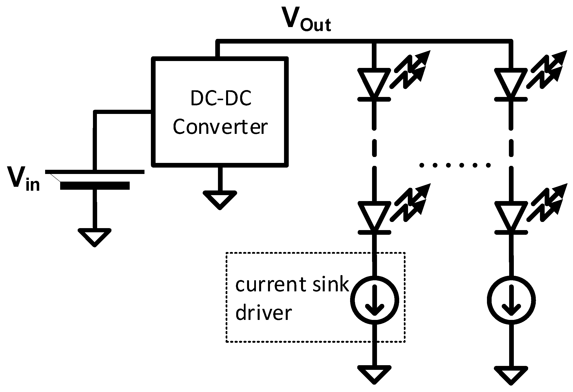
:1. Introduction
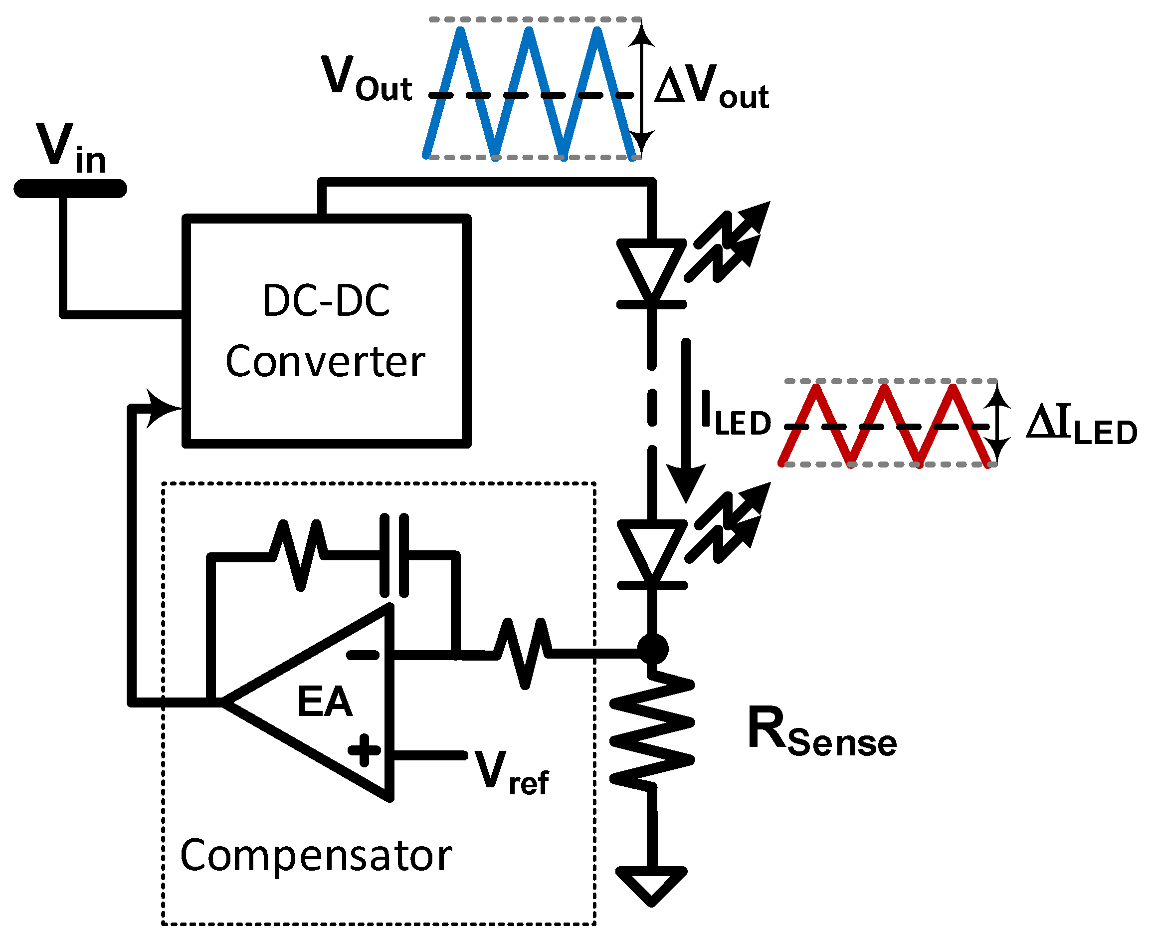
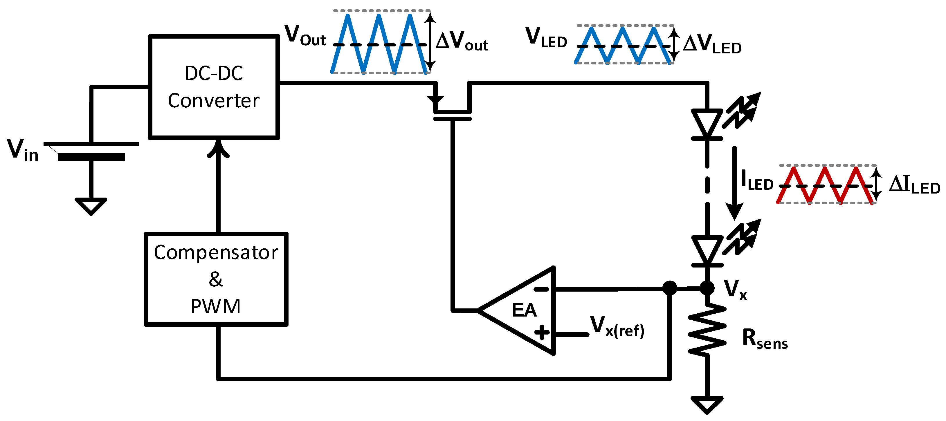
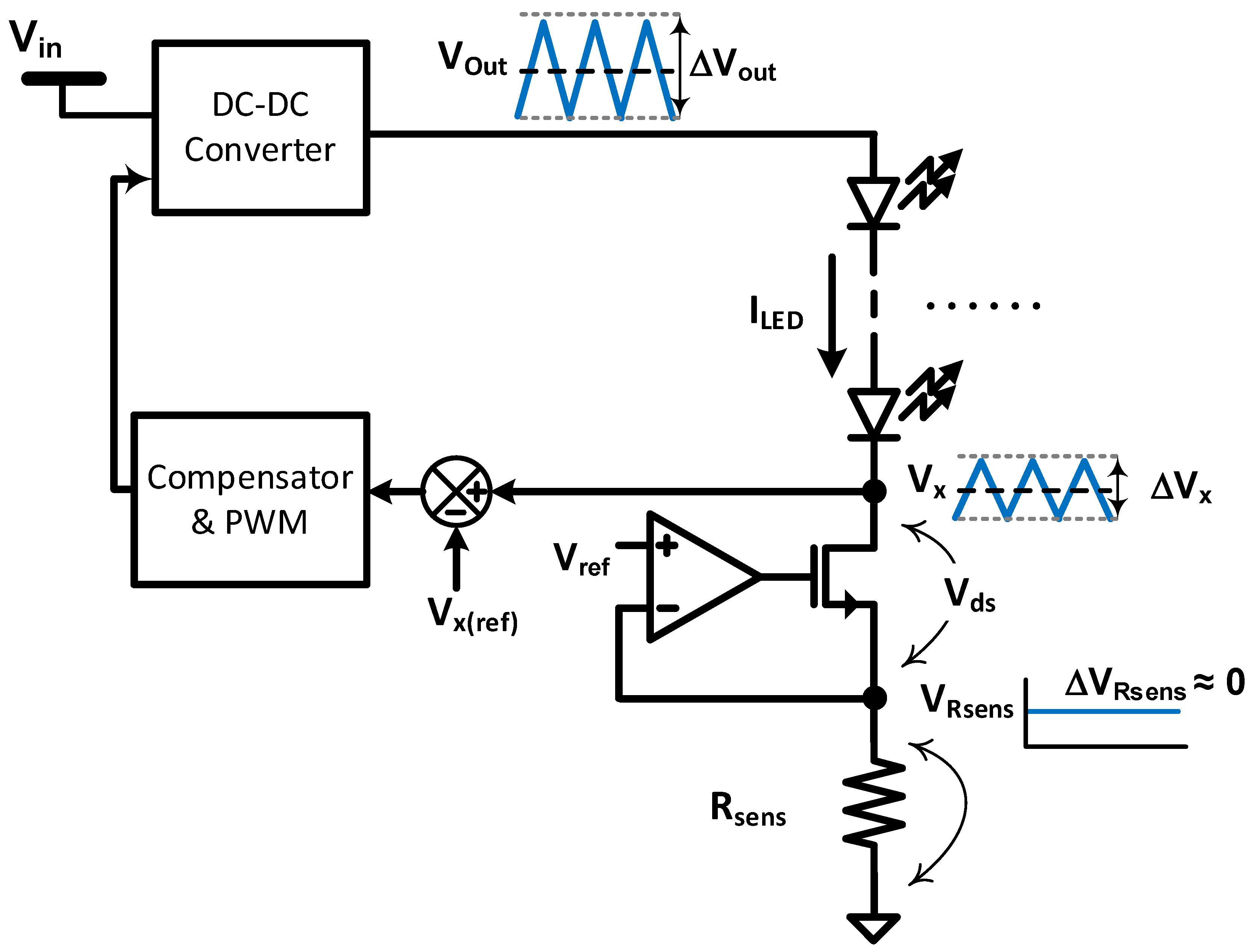
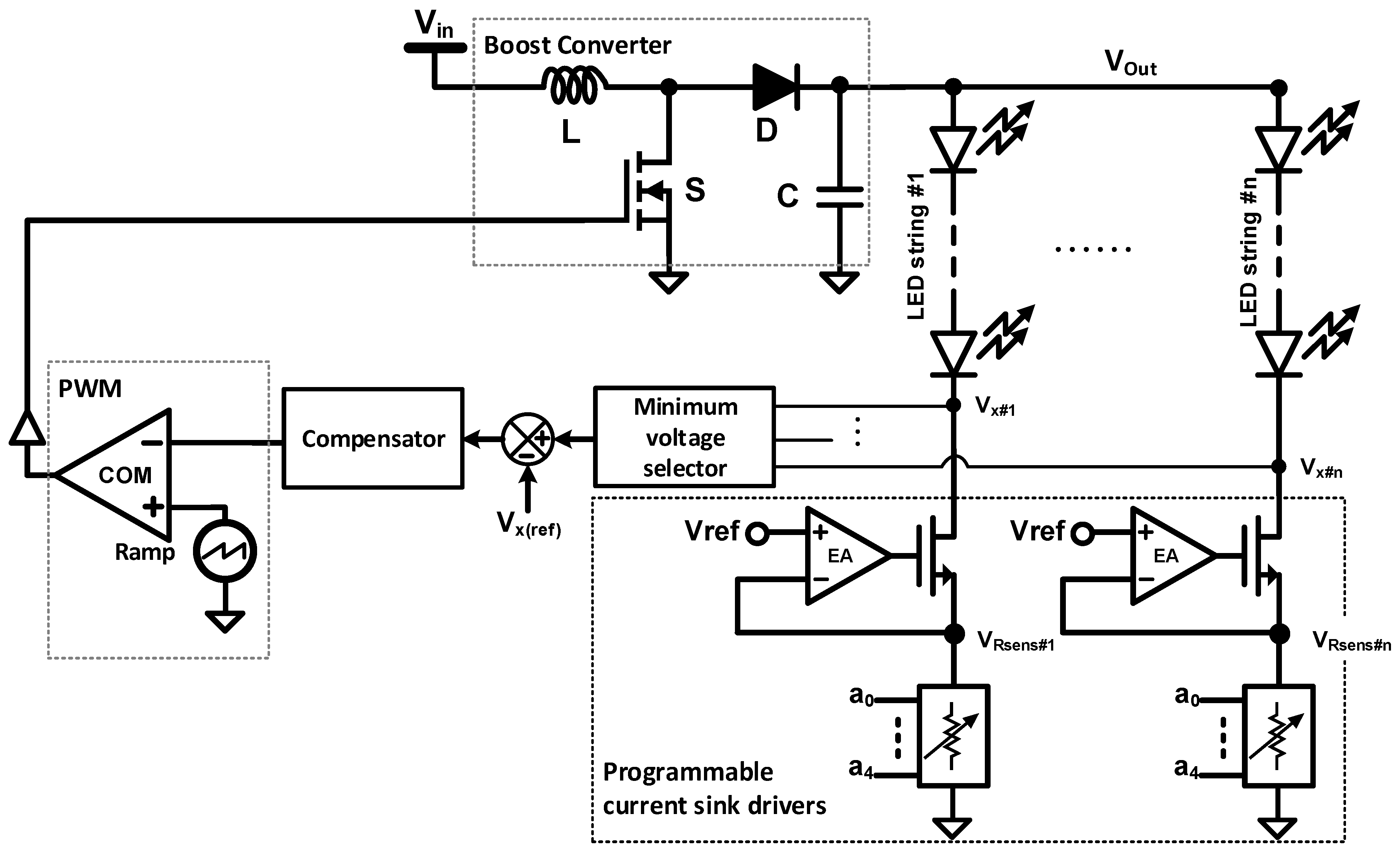
2. Programmable Resistor Current Sink Topology
3. Design Methodology and an Application Example Simulation
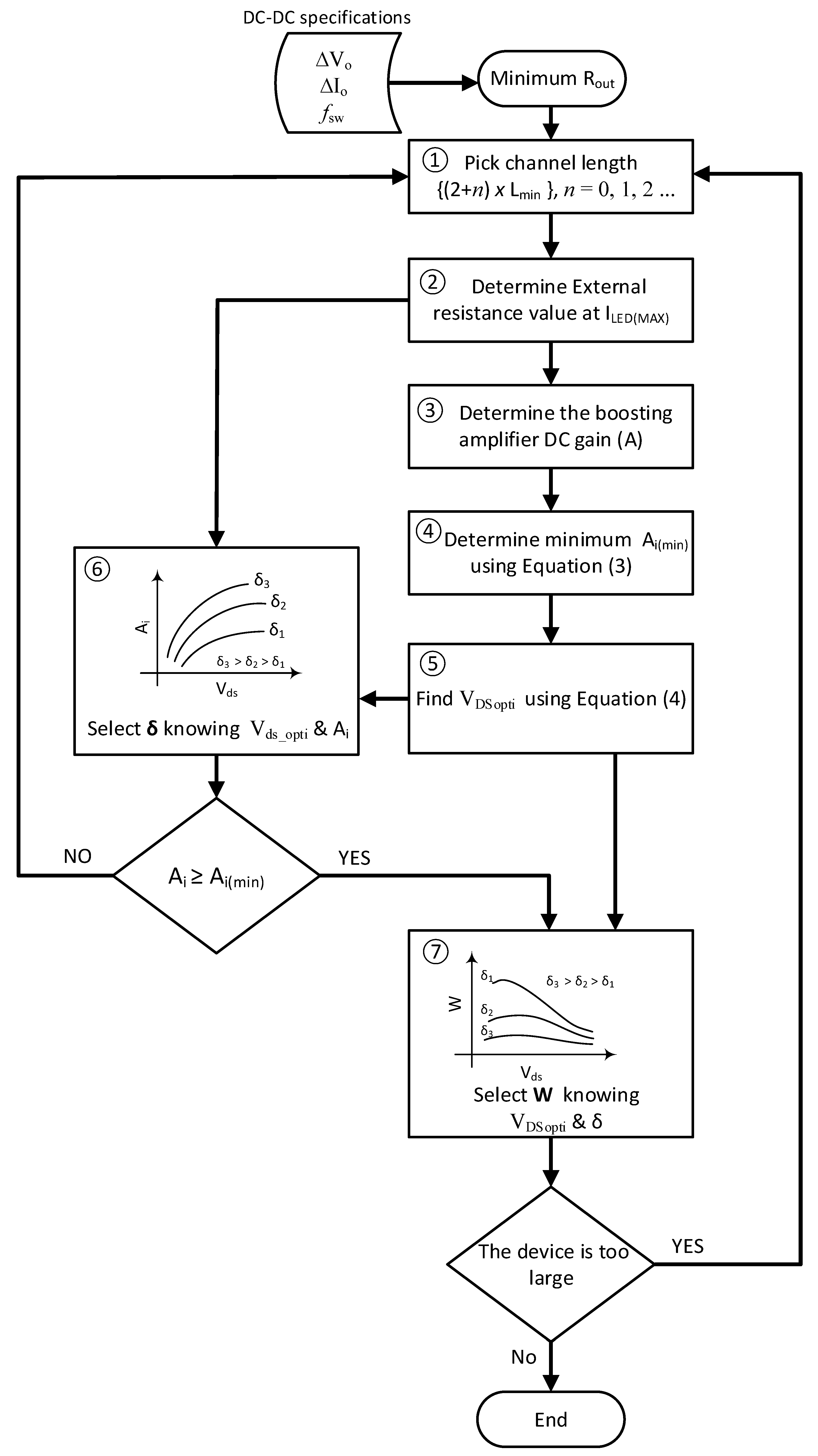
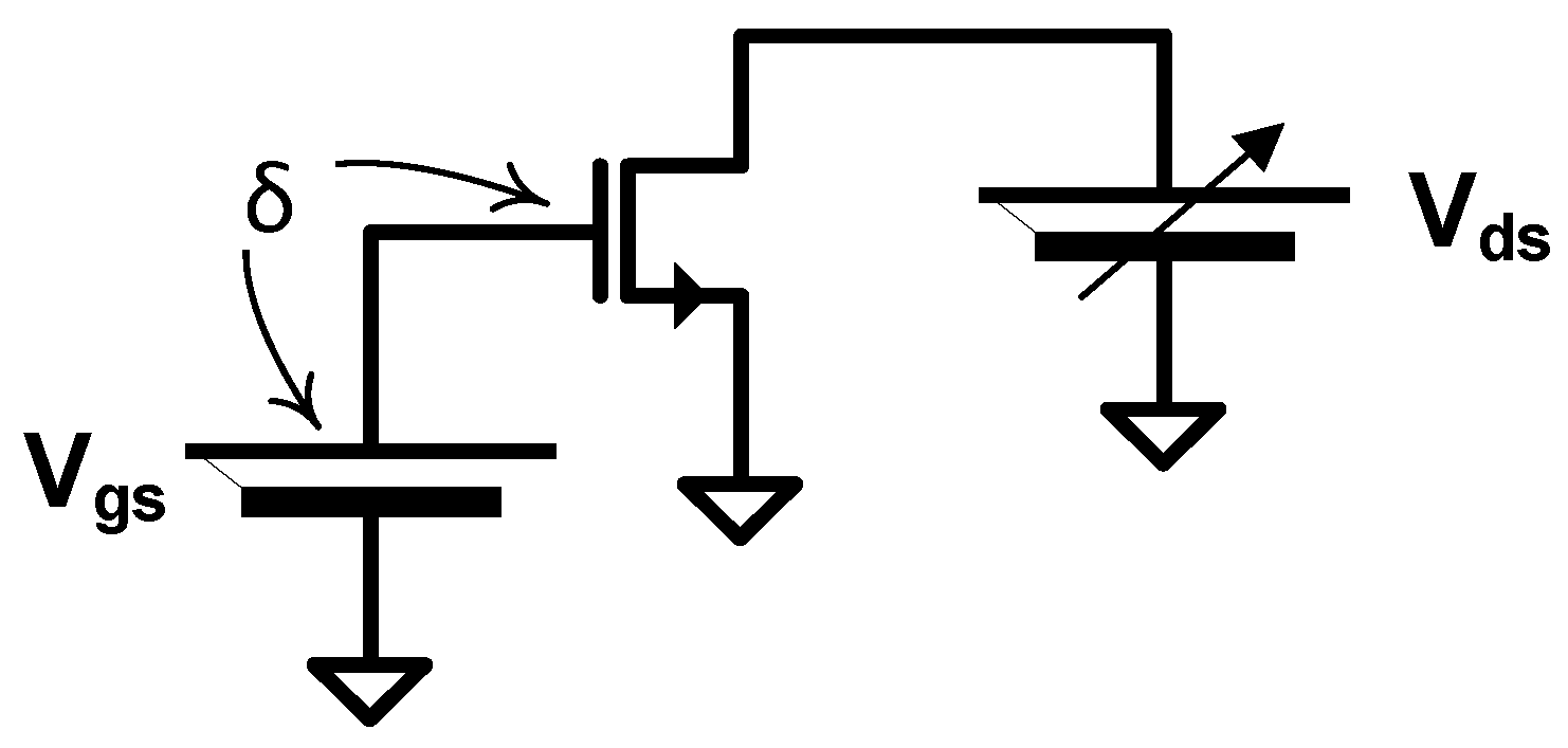
3.1. Design Methodology
3.2. WLED Design Example
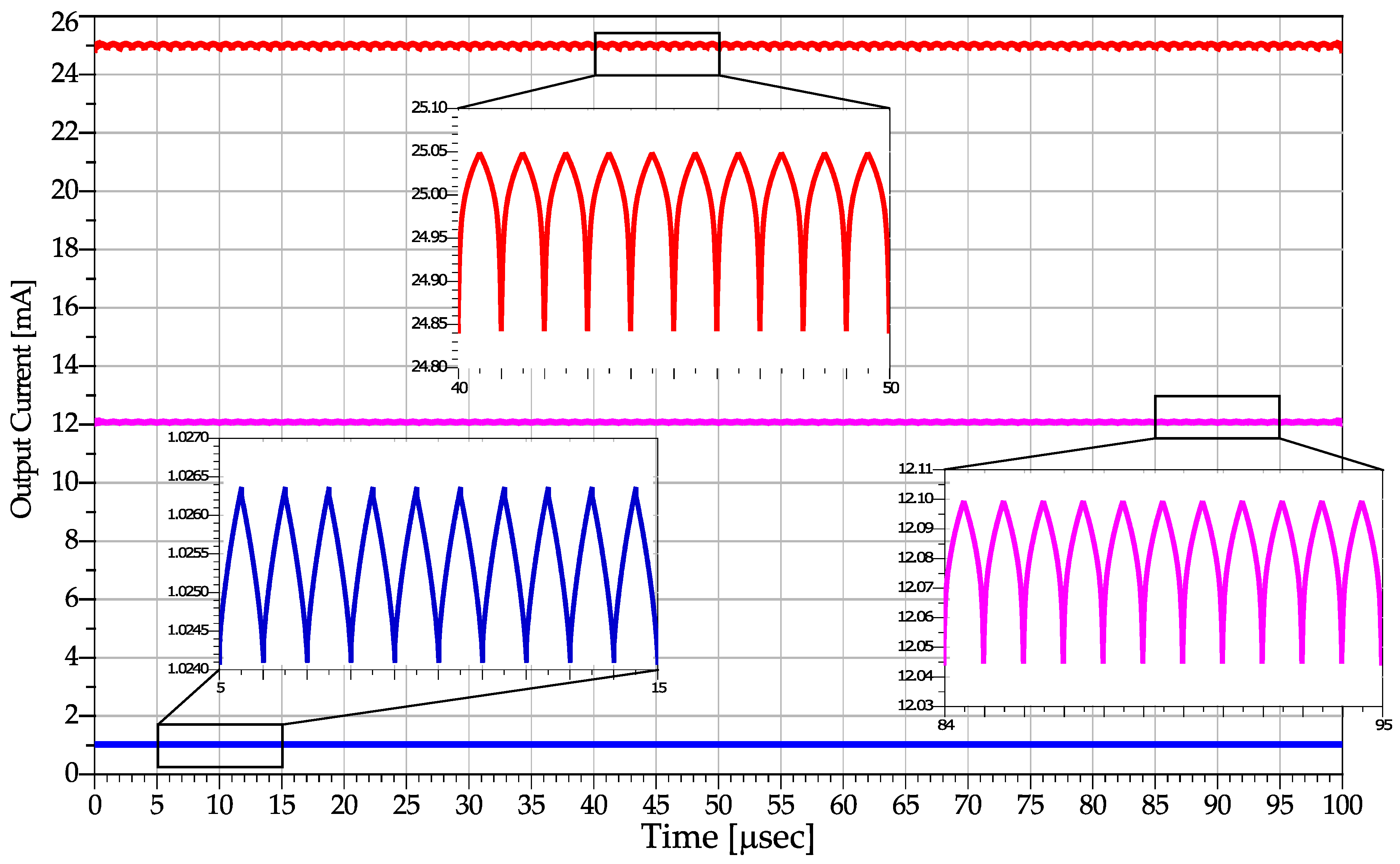
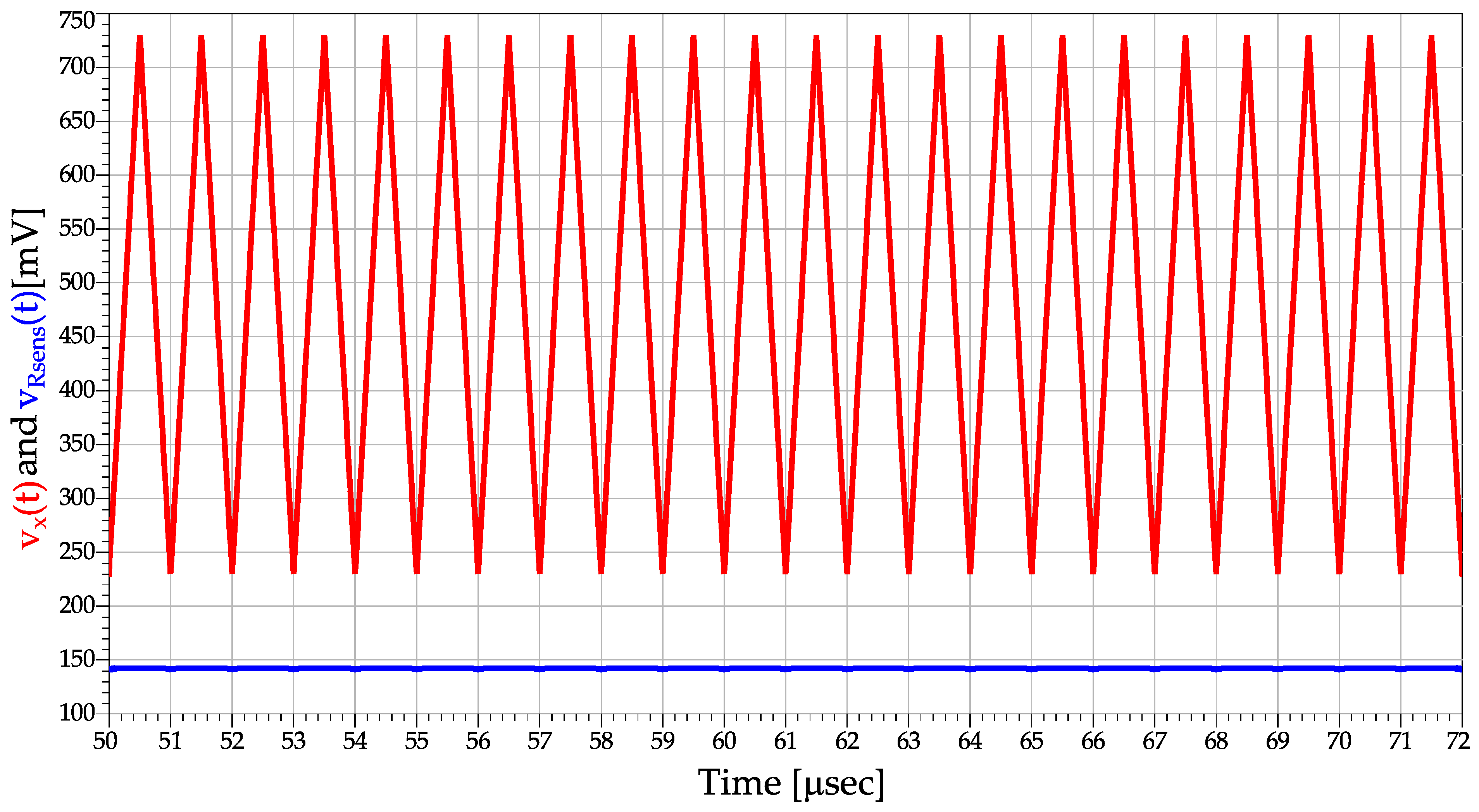
3.3. Simulation Results
4. Conclusions
Author Contributions
Funding
Data Availability Statement
Acknowledgments
Conflicts of Interest
References
- Yoon, S.-J.; Cho, J.-K.; Hwang, I.-C. High efficiency multi-channel LED driver IC with low current-balance error using current-mode current regulator. J. Electr. Eng. Technol. 2017, 12, 1593–1599. [Google Scholar]
- Kuo, T.-H.; Liang, T.-J.; Wu, W.-J. Design and implementation of a LED driver with current balancing. In Proceedings of the 2016 IEEE 8th International Power Electronics and Motion Control Conference (IPEMC-ECCE Asia), Hefei, China, 22–26 May 2016; pp. 3306–3313. [Google Scholar]
- Hu, Y.; Jovanovic, M.M. LED driver with self-adaptive drive voltage. IEEE Trans. Power Electron. 2008, 23, 3116–3125. [Google Scholar] [CrossRef]
- Eguchi, K.; Shibata, A.; Asadi, F.; Ishibashi, T.; Harada, Y.; Oota, I. Design of an LED Sink Driver Using a Switched-Inductor and Switched-Capacitor Buck-Boost Converter with High Voltage Gains. In Proceedings of the 2020 2nd International Conference on Smart Power & Internet Energy Systems (SPIES), Bangkok, Thailand, 15–18 September 2020; pp. 33–38. [Google Scholar]
- Yang, D. SoC scaling challenges in the era of the single digit technology nodes. In Proceedings of the Presented at the International Workshop Advanced Patterning Solutions, Chengdu, China, 12–13 October 2017; pp. 1–10. [Google Scholar]
- Loke, A.L.; Yang, D.; Wee, T.T.; Holland, J.L.; Isakanian, P.; Rim, K.; Yang, S.; Schneider, J.S.; Nallapati, G.; Dundigal, S.; et al. Analog/mixed-signal design challenges in 7-nm CMOS and beyond. In Proceedings of the 2018 IEEE Custom Integrated Circuits Conference (CICC), San Diego, CA, USA, 8–11 April 2018; pp. 1–8. [Google Scholar]
- Ahmad, H.H.; Shahroury, F.R. Design of a High Efficiency WLED Driver in 40 nm CMOS Technology. In Proceedings of the 2020 32nd International Conference on Microelectronics (ICM), Aqaba, Jordan, 14–17 December 2020; pp. 1–4. [Google Scholar]
- Ahmad, H.H.; Shahroury, F.R.; Abuishmais, I. A Multi-Output Multi-String High-Efficiency WLED Driver Using 40 nm CMOS Technology. J. Low Power Electron. Appl. 2021, 11, 47. [Google Scholar] [CrossRef]
- Yang, L.; Yu, W.; Zhang, J. Variable frequency constant current control method for switched-capacitor converter based automotive LED driver. IEEE Access 2019, 7, 42094–42106. [Google Scholar] [CrossRef]
- Ye, C.; Das, P.; Sahoo, S.K. Peak current control of multichannel LED driver with selective dimming. IEEE Trans. Ind. Electron. 2018, 66, 3446–3457. [Google Scholar] [CrossRef]
- Ye, C.; Chan, H.W.; Lan, D.; Das, P.; Sahoo, S.K. Efficiency improvement of multichannel LED driver with selective dimming. IEEE Trans. Power Electron. 2019, 35, 6280–6291. [Google Scholar] [CrossRef]
- Qu, Y.; Wang, Z. Soft-switching techniques for single-inductor multiple-output led drivers. IEEE Trans. Power Electron. 2020, 35, 13748–13756. [Google Scholar] [CrossRef]
- Sunny, L.; Philip, P. Flicker free LED backlight driver with Passive Current Balancing and dimming function. In Proceedings of the 2021 International Conference on Communication, Control and Information Sciences (ICCISc), Idukki, India, 16–18 June 2021; Volume 1, pp. 1–6. [Google Scholar]
- Wong, C.S.; Loo, K.H.; Iu, H.H.-C.; Lai, Y.M.; Chow, M.H.L.; Chi, K.T. Independent control of multicolor-multistring LED lighting systems with fully switched-capacitor-controlled LCC resonant network. IEEE Trans. Power Electron. 2017, 33, 4293–4305. [Google Scholar] [CrossRef]
- Wu, C.-H.; Chen, C.-L. High-efficiency current-regulated charge pump for a white LED driver. IEEE Trans. Circuits Syst. II Express Briefs 2009, 56, 763–767. [Google Scholar]
- Hsu, Y.-C.; Lin, J.-Y.; Chen, C.C.-P. Area-saving and high-efficiency RGB LED driver with adaptive driving voltage and energy-saving technique. Energies 2018, 11, 1422. [Google Scholar] [CrossRef]
- Yang, W.-H.; Yang, H.-A.; Huang, C.-J.; Chen, K.-H.; Lin, Y.-H. A high-efficiency single-inductor multiple-output buck-type LED driver with average current correction technique. IEEE Trans. Power Electron. 2017, 33, 3375–3385. [Google Scholar] [CrossRef]
- Yang, Y.; Ruan, X.; Zhang, L.; He, J.; Ye, Z. Feed-forward scheme for an electrolytic capacitor-less AC/DC LED driver to reduce output current ripple. IEEE Trans. Power Electron. 2013, 29, 5508–5517. [Google Scholar] [CrossRef]
- Shahroury, F.R.; Ahmad, H.H.; Abuishmais, I. Design Aspects of a Single-Output Multi-String WLED Driver Using 40 nm CMOS Technology. J. Low Power Electron. Appl. 2022, 12, 5. [Google Scholar] [CrossRef]
- Meraj, M.; Rahman, S.; Iqbal, A.; Ben-Brahim, L. High brightness and high voltage dimmable LED driver for advanced lighting system. IEEE Access 2019, 7, 95643–95652. [Google Scholar] [CrossRef]
- Hsieh, H.-I.; Wang, H. LED Current Balance Using a Variable Voltage Regulator with Low Dropout vDS Control. Appl. Sci. 2017, 7, 206. [Google Scholar] [CrossRef]
- Hsieh, Y.-T.; Liu, B.-D.; Wu, J.-F.; Fang, C.-L.; Tsai, H.-H.; Juang, Y.-Z. A high-dimming-ratio LED driver for LCD backlights. IEEE Trans. Power Electron. 2012, 27, 4562–4570. [Google Scholar] [CrossRef]
- Yao, K.; Moyer, J.C. Control of Multi-String LED Array. U.S. Patent 8,410,716, 2 April 2013. [Google Scholar]
- Sedra, A.S.; Smith, K.C.; Carusone, T.C.; Gaudet, V. Microelectronic Circuits; Oxford University Press: New York, NY, USA, 2004; Volume 4. [Google Scholar]
- Jaradat, R.O.; Shahroury, F.R.; Ahmad, H.H.; Abuishmais, I. Design methodology for narrow-band low noise amplifier using CMOS 0.18 μM technology. Jordanian J. Comput. Inf. Technol. 2022, 8. [Google Scholar] [CrossRef]
- Shahroury, F.R.; Riad, I. The design and optimization of low-voltage pseudo differential pair operational transconductance amplifier in 130 nm cmos technology. In Proceedings of the 2016 UKSim-AMSS 18th International Conference on Computer Modelling and Simulation (UKSim), Cambridge, UK, 6–8 April 2016; pp. 361–365. [Google Scholar]
- Allen, P.E.; Holberg, D.R. CMOS Analog Circuit Design; Elsevier: Amsterdam, The Netherlands, 2011. [Google Scholar]


| Topology | Size (1) | Efficiency (1) | Integrability | Complexity | Sensitivity to Current Ripple (2) |
|---|---|---|---|---|---|
| Sensing resistor current sink driver | Small | Low | Hard | Simple | Very sensitive |
| PMOS-based current sink driver | Large | Moderate | Very hard | Complex | Sensitive |
| NMOS-based current sink driver | Medium | High | Easy | Moderate | Less sensitive |
| Parameter | Values |
|---|---|
| Input voltage (a) | 3.2–4.2 V |
| WLED string current | 1–25 mA (dimmable) |
| Current resolution | 1 mA |
| Current ripple | <1% |
| String arrangement | 6 WLEDs |
| WLED forward voltage drop | 3.2 V |
| Output voltage ripple | <2.5% |
| Op-amp quiescent current | 100 µA |
| Switching frequency | 1 MHz |
| GBP | 100 MHz |
| Efficiency (of current driver) | >97% |
Publisher’s Note: MDPI stays neutral with regard to jurisdictional claims in published maps and institutional affiliations. |
© 2022 by the authors. Licensee MDPI, Basel, Switzerland. This article is an open access article distributed under the terms and conditions of the Creative Commons Attribution (CC BY) license (https://creativecommons.org/licenses/by/4.0/).
Share and Cite
Abuishmais, I.; Shahroury, F.R.; Ahmad, H. A Design Methodology of High-Efficiency Dimmable Current Sink for Current-Regulated Drivers. Electronics 2022, 11, 2566. https://doi.org/10.3390/electronics11162566
Abuishmais I, Shahroury FR, Ahmad H. A Design Methodology of High-Efficiency Dimmable Current Sink for Current-Regulated Drivers. Electronics. 2022; 11(16):2566. https://doi.org/10.3390/electronics11162566
Chicago/Turabian StyleAbuishmais, Ibrahim, Fadi R. Shahroury, and Hani Ahmad. 2022. "A Design Methodology of High-Efficiency Dimmable Current Sink for Current-Regulated Drivers" Electronics 11, no. 16: 2566. https://doi.org/10.3390/electronics11162566
APA StyleAbuishmais, I., Shahroury, F. R., & Ahmad, H. (2022). A Design Methodology of High-Efficiency Dimmable Current Sink for Current-Regulated Drivers. Electronics, 11(16), 2566. https://doi.org/10.3390/electronics11162566