Article

Electromagnetic Simulation Flow for Integrated Power Electronics Modules

1
STMicroelectronics, 95100 Catania, Italy
2
Department of Electrical Electronic and Computer Engineering (DIEEI), University of Catania, 95125 Catania, Italy
*
Author to whom correspondence should be addressed.
Electronics 2022, 11(16), 2498; https://doi.org/10.3390/electronics11162498
Submission received: 29 June 2022 / Revised: 29 July 2022 / Accepted: 5 August 2022 / Published: 10 August 2022

Abstract

:
The growing use of electric vehicles is requiring the implementation of power electronics applications with ever faster devices, such as silicon carbide (SiC) MOSFET, to reduce switching power losses and reach higher power density, with the final objective of improving performance and lowering the system cost. A side effect of such faster switching devices is the generation of high-frequency harmonics with significant energy, so their impact must be evaluated in terms of conducted and radiated electromagnetic interference (EMI). The optimal design of PCBs and filters for facing electromagnetic compatibility issues requires properly estimating the EMI level of different design solutions. Analysis of the current state of the art reveals that previous approaches can not effectively support a design focusing on a reduction in radiated EMI. To surpass these limits, the paper defines an electromagnetic simulation flow aimed at evaluating the radiative fields in the case of an integrated power electronics module operating in automotive applications and featuring fast SiC power devices. Then, the proposed simulation was applied to an LLC resonant converter featuring an STMicroelectronics SiC-based ACEPACK module. The work also highlights that future research efforts must concentrate on finding the best compromise between computational effort and estimation accuracy.

1. Introduction

The need for cleaner vehicles is leading to the growing usage of power electronics inside vehicles aimed at managing significant amounts of power, often higher than tens of kW. Newer and faster power devices such as silicon carbide (SiC) MOSFETs are destined to become the heart of the power stages of hybrid electric vehicles (HEVs). SiC devices can switch at higher frequencies and improve system efficiency. On the other hand, faster switching means higher current and voltage slopes inside application circuitries, and the related radiative effects could become an important aspect to be analysed and pondered [1,2]. Among the several solutions adopted for managing large power amounts, the one based on integrated power electronics modules (IPEMs) (Figure 1) is very effective in the control of thermal aspects [3]. IPEMs can usually be built by adopting several technologies on the basis of different solutions such as discrete components on insulated-metal substrates (IMS), dices on IMS, or substrate-free molded structures according to the context in which they have to be used.
While electromagnetic simulation flows aimed at evaluating electromagnetic related phenomena were extensively studied in the literature [4,5,6,7,8], their specific application in IPEMs or power modules is less examined or often limited to electromagnetic compatibility (EMC) aspects [9]. In some cases, electromagnetic (EM) evaluation is performed through mathematical models able to predict EM interference (EMI) phenomena [4] or through a classical measurement approach [10] with all the issues related to the need for a prototype and an anechoic chamber.
An accurate electromagnetic simulation flow that can predict radiative phenomena without the need for a physical prototype can be extremely useful, since alternatives can be evaluated at the design stage, thus avoiding redesign and fabrication costs, and time-to-market delays that are caused by an eventual failure of the compliance tests.
This paper outlines an electromagnetic simulation flow able of providing accurate results on the radiated field in the case of an HEV application exploiting an LLC resonant converter featuring an IPEM that uses SiC MOSFET devices in a half-bridge configuration. The paper is divided into two parts. The first one provides an overview of previous works on EMC/EMI phenomena and an analysis of their limits. Then, the proposed electromagnetic simulation flow is discussed. The second part describes the simulation workflow in an actual power module where the radiated emissions are estimated by using the proposed approach. Lastly, this case study raises the issues in using the proposed approach that requires future research efforts.

2. Radiated EMI Estimation for the Optimal Design

The optimal design of PCBs and filters requires the correct assessment of the EMI level for different design solutions. This estimation, in turn, requires the use of appropriate techniques and tools able to compute the EMI expected from different design solutions. When these techniques are based on experimental results, the optimal design leads to high development costs and time. To reduce the time to market and to analyse a large number of different design solutions with inexpensive effort, an appropriate technique must rely only on simulation tools. From this perspective, when integrated power electronics modules are considered, a proper electromagnetic simulation flow that does not need measurements is essential. One of the most relevant aspects of this work is that it mainly emphasizes the phenomenon of radiated emissions with respect to conducted emissions. This strategy was adopted to tune the simulation flow using a complete set of waveforms and not a filtered one as it is usually performed by firstly minimizing conducted emissions and consequently also radiated ones [9,11]. This preventive filtering of conducted emissions risks makes less appreciable the levels of emissions radiated by the system, therefore making the simulation flow harder to set up due to the system being less sensitive to the radiative phenomenon. It is for this reason that we analyse the tested device without having previously optimized the conducted emissions. It should certainly not be surprising that this assumption could make the system noncompliant with current regulations.
With all this in mind, in the following, the literature is analysed to highlight the limits of previous approaches. After that, the proposed electromagnetic simulation flow that overpasses these limits is described.

2.1. Related Papers

The work in [12] is one of the first papers proposing an exclusively simulation-based evaluation of electromagnetic interference due to switching power converters, although it only focused on conducted emissions.
Some parasitic components of boards and devices were combined with simplified switching waveforms to estimate electromagnetic radiation [13]. That method enables only a good estimation of noise waveforms that are expected to be the source of radiated EMI, but it does not evaluate them. A circuit simulation tool was proposed in [14] to evaluate the switching voltage waveforms in SiC MOSFET power modules. The waveforms of the voltage at the input and output of the converter were estimated to simulate the EMI due to cables, while the EMI due to the converter was not investigated. Similarly, a computationally efficient method for the wideband modelling and simulation of the voltage and current in medium-voltage DC railway systems was proposed in [15] as a necessary step for the assessment of conducted EMI during the project design stage, but it was not used to foresee radiated EMI.
A procedure to foresee electromagnetic disturbances was suggested in [6]. The need for near-field measurements is a limitation at the design stage. Another approach based on near-field measurements for modelling the electromagnetic emissions of PCBs was proposed in [16]. The method can be used when simple PCB structures are considered and does not consider power converters. A method for modelling the sources of electromagnetic disturbance due to power electronic equipment was discussed in [17]. It is based on near-field measurement like the previous one; thus, it presented similar limitations.
A method that models the common-mode current with a radiation source and the cable bundle with elementary dipoles to compute field emissions was discussed in [7]. That work also presented a method that only uses common mode current and transmission line parameters for field emissions. However, also this method requires measurements in an anechoic shielded chamber.
An advanced version of multiple-segment transfer functions, including a current distribution algorithm without the need for extra phase information, was presented in [18]. Those current distributions in combination with multiple transfer functions are used in that work to calculate the electrical field. However, the method used common-mode currents on the cable harness and it did not consider power converters. A method similar to the previous one was applied to an inverter in [19]. However, it was based on two transfer functions whose parameters were obtained from current measurements.
The numerical prediction of radiated emissions from a PCB segment was performed in [4]. On the other hand, typical excitations due to switching devices and the multiple traces usually present in a power converter were not considered. A field prediction method that combines a measured common-mode current distribution with numerical computations for the radiated fields in the frequency range of 30–1000 MHz was presented in [5]. The method focused only on the radiation from the cable bundle, and the need for measurements impeded its use at the design stage. In [20], the radiated emission from cables was simulated using HFSS. The converter model was combined with the model of the antenna equivalent to the behaviour of the cable. The weakness of the approach is that it needed the measurements of the switching voltages related to the power converter devices. Moreover, the parasitic components of the PCB were not considered. Lastly, only the radiated EMI of the cable was considered, while that related to the converter was neglected. Similarly, the authors in [21] focused only on the prediction of radiated EMI due to the cable.
An analytical method for calculating parasitic components was combined with finite-difference time-domain simulation in [22] to calculate the near magnetic field emitted by the power supply cable of a buck converter. The measured drain-to-source voltage was necessary for the model, which implemented the waveform in a voltage source to account for MOSFET contribution to EMI.
A terminal equivalent circuit model for estimating radiated EMI from the cables connected to the terminals of DC–DC converters was proposed in [23]. The first step to obtaining the model requires the measurement of the input and output common-mode currents and the drain-source voltage with varying loads. To minimize the EMI in a buck converter, a new structure and control based on a combination of two techniques was proposed in [24]. To this aim, a simple analysis was performed using circuit simulation to foresee the conducted EMI, while the radiated EMI was neglected. In view of EMI evaluations, a modelling method of buck converter IC based on the analysis of noise path was proposed in [25] so that the switching voltage from buck converter can be estimated and simulated faster and simpler without using SPICE models. Although the model is interesting, it has not been actually used for EMI estimation. The finite-element simulation was adopted in [26] to design a low-inductance busbar to reduce high-frequency EMI and voltage overshoot in an active neutral point clamped DC-DC converter undergoing zero-voltage switching. EMI performance (conducted and radiated) was experimentally validated for two of the most useful switching schemes. Once again, the need for experimental measurements to evaluate EMI was the main limitation.
The optimal design of an on-board charger in terms of satisfying EMC limits was introduced in [9]. To this aim, that work explained a method to integrate electromagnetic simulation and measurements. Therefore, it highlighted the strength of the use of electromagnetic simulation for the computer-aided design of a shield, but it needed some measurements for radiated emission analysis.
An electromagnetic simulation framework to generate system-level EMC results was proposed in [27]. Current and voltage were extracted using the measurement method specified in IEC 61967-4. The waveforms were then used in a mixed model to foresee EMI.
Radiated EMI due to the voltage between input and output cables in a nonisolated power converter was investigated in [28]. The radiated EMI model of a nonisolated power converter was presented on the basis of circuit topologies, PCB parasitics, switching waveforms, and transfer functions. The measured waveforms of currents and voltages of switches and diodes were used for radiated EMI prediction.
EMI prediction is essential during the optimal design of a power converter aiming at reducing the radiated EMI, but the analysis of previous works in this field revealed that they usually present one or more of the following limitations.
  • The need for measurements.
  • The estimation of only the EMI source (e.g., simulation of the switching waveforms).
  • The prediction of radiated EMI due to only the cables.
The simulation flow for radiated EMI estimation described in Section 2.2 surpasses these limitations.

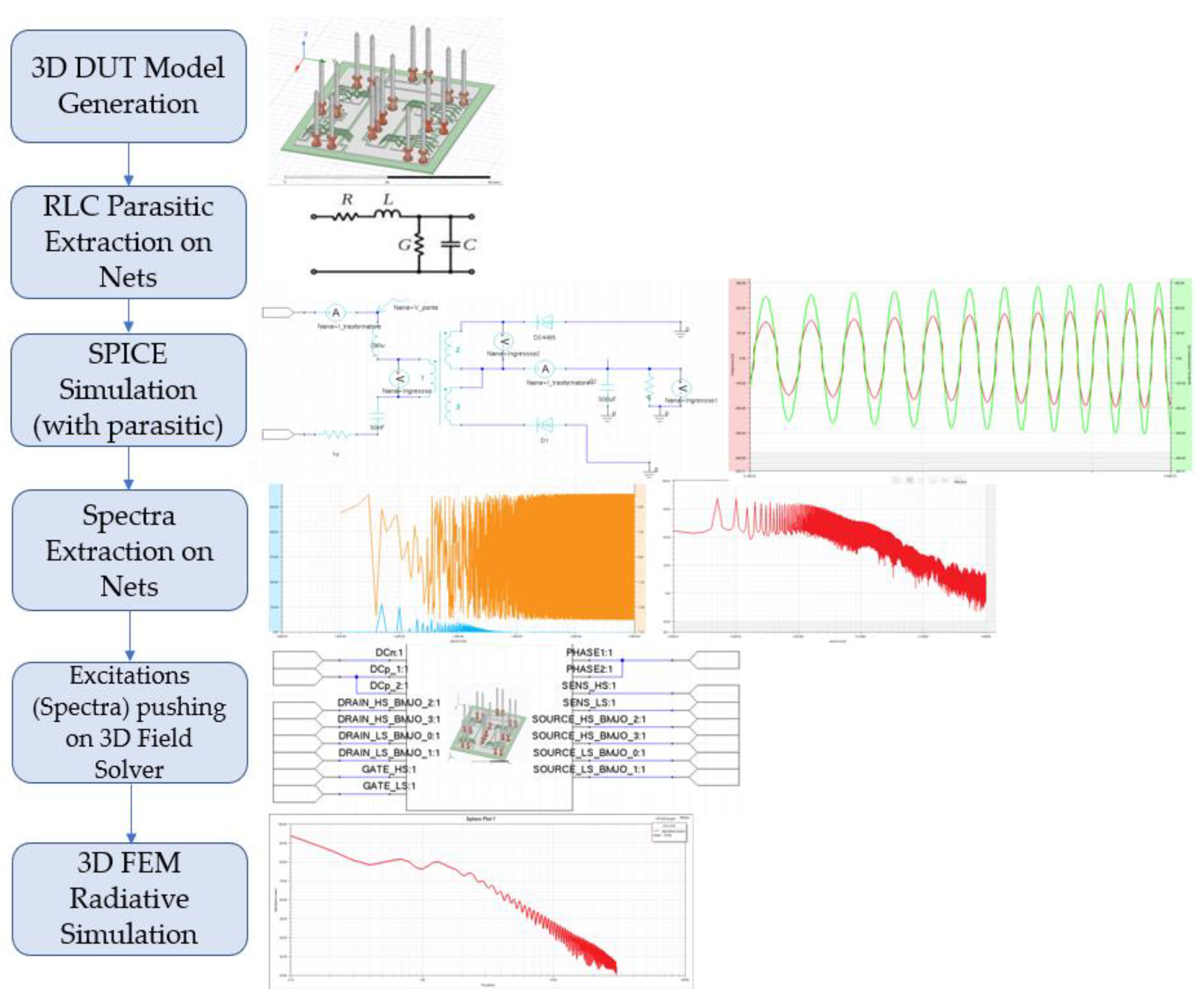
2.2. Proposed Simulation Flow for Raiated EMI Prediction

In order to predict EMI phenomena in electronics systems, a computer-aided design (CAD) workflow was implemented. A key aspect of the proposed flow (Figure 2) relies on the possibility of generating signal spectra that represent the electric fields radiated by devices; this approach would allow for reducing measurements in an anechoic chamber, which is often complex to accomplish. Moreover, increasingly stringent radiative limits imposed by regulations require predictive approaches to reduce the time to market for the system under development.
The flow starts by reproducing the 3D geometry of the system to be simulated (3D DUT Model Generation) by creating 3D structure of connectors, vias, wire bonds, solder balls, signal traces, power, ground planes and so on. During this step, details about materials must also be provided to the tool. Then, the CAD drawing is provided to a quasistatic EM simulator to extract the parasitic contributions of interconnections (RLCs). During this step, the input and output ports of the system must also be defined and assigned to specific physical areas of the structure.
Once the parasitic contributions are evaluated, they are associated with the circuit models of the discrete power devices. A transient simulation is then performed to obtain the simulation waveforms representing realistic ones. The waveforms obtained in the time domain are then expressed in terms of electrical spectra by applying Fourier analysis. For example, the voltage waveforms between the nodes (nets) of one device are represented by these spectra. The spectra are, in turn, the input (excitation pushing) for the final radiative electromagnetic simulation that must be performed by a full-wave FEM tool. Once the FEM simulation is completed, the radiated electrical field at several distances from the system can be plotted.
It is worth highlighting that circuit simulator results are implicitly related to the conducted emission that the system is undergoing. Hence, a preliminary idea about the noise on the system nets arises from their evaluation, thus allowing for a preliminary check of harmonics with high energy levels. Figure 3 shows that the noise at first harmonics (50 and 100 kHz) is around ~170 dBuV, a non-negligible quantity of energy, meaning that attenuation is necessary.

3. Case Study

The general flow described in the previous section was customized for an application featuring an integrated power electronics module produced by STMicroelectronics (ACEPACK). We describe every step by providing the relevant information concerning the implementation phase. The module itself is part of a complex system belonging to the automotive application field.

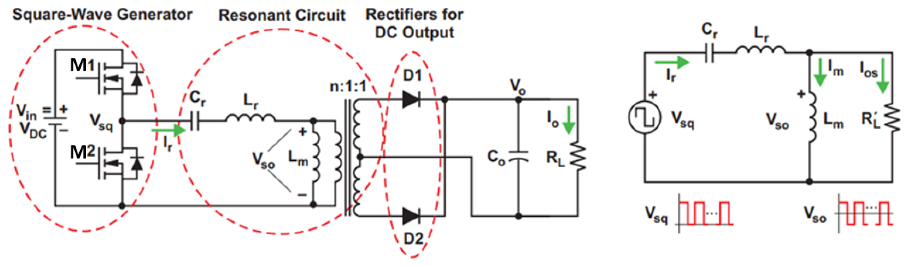
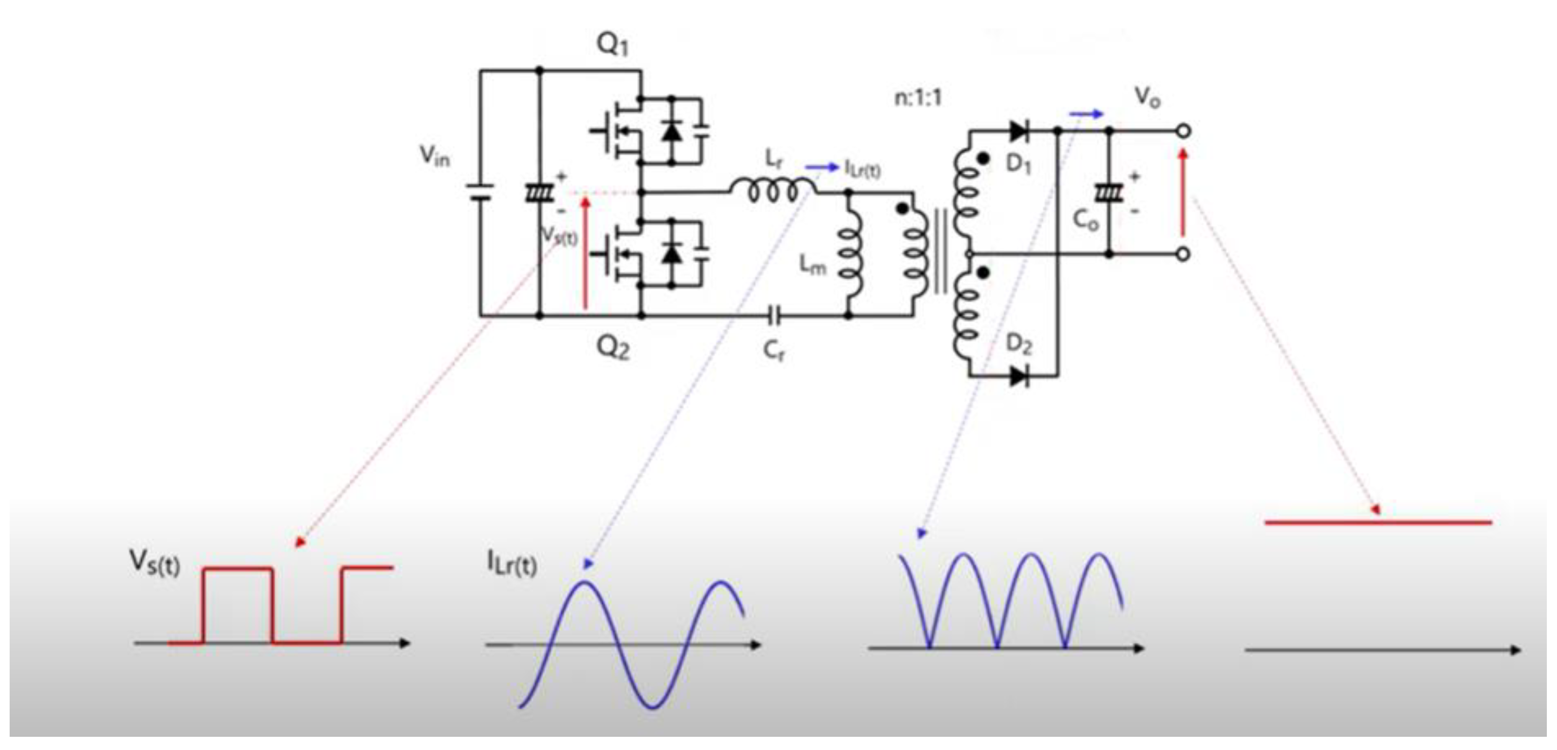
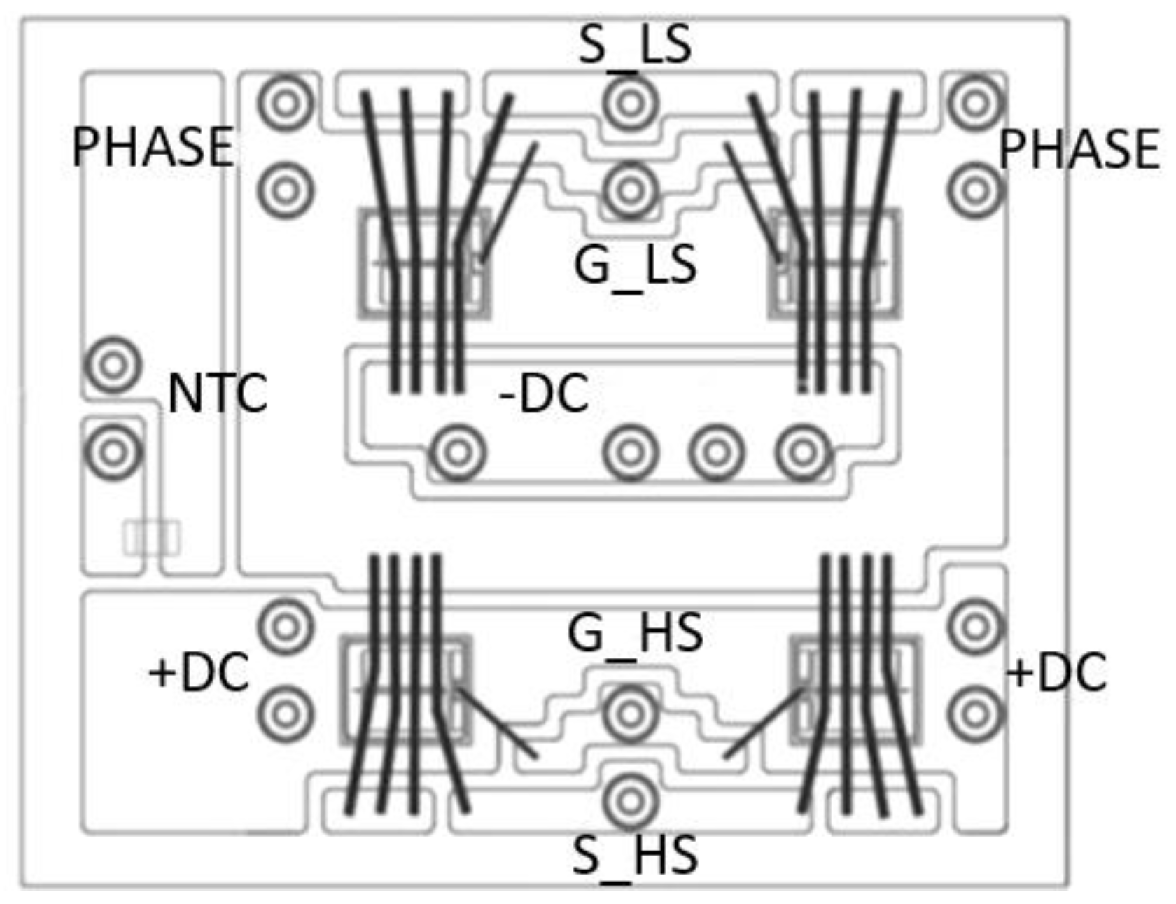
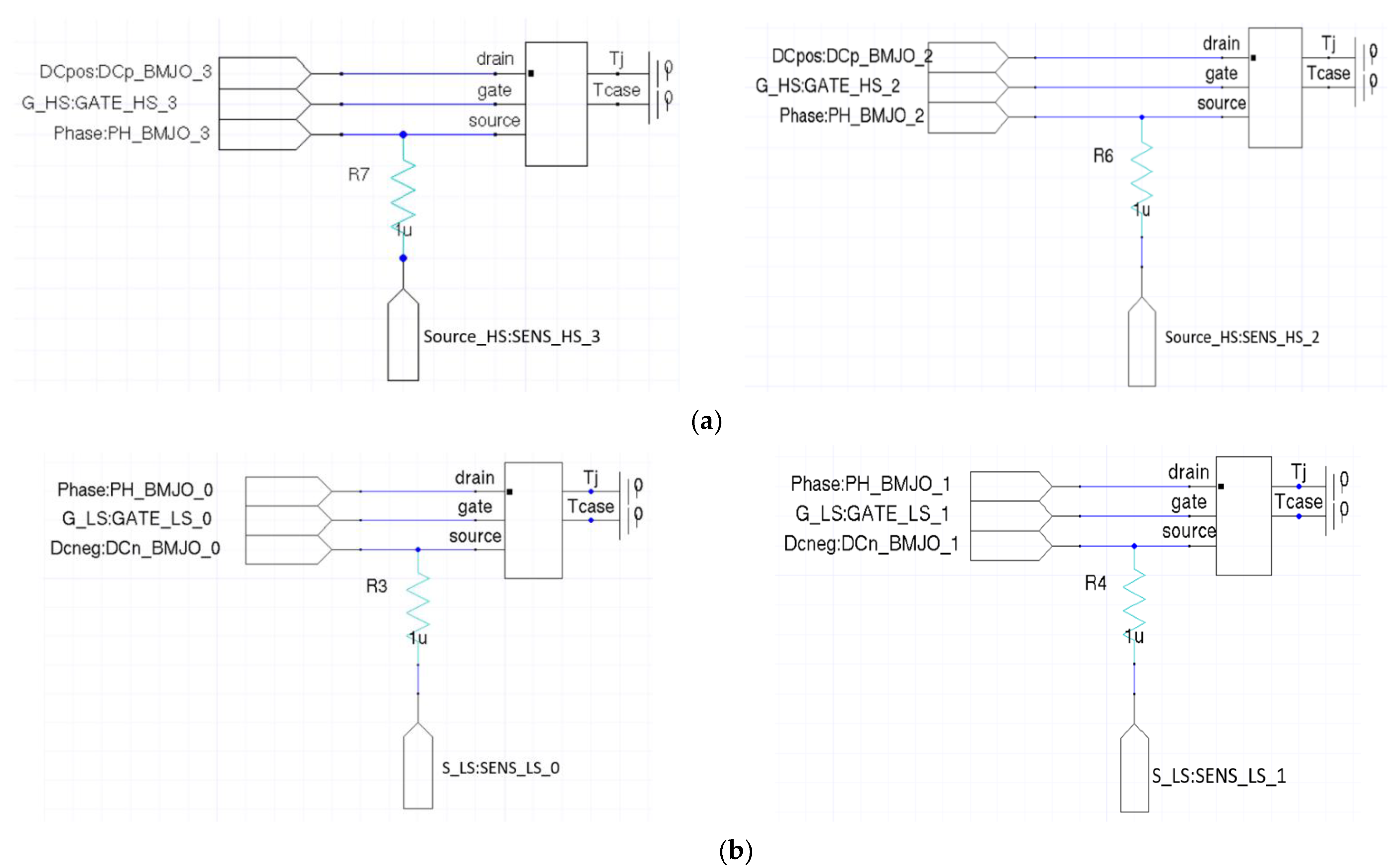
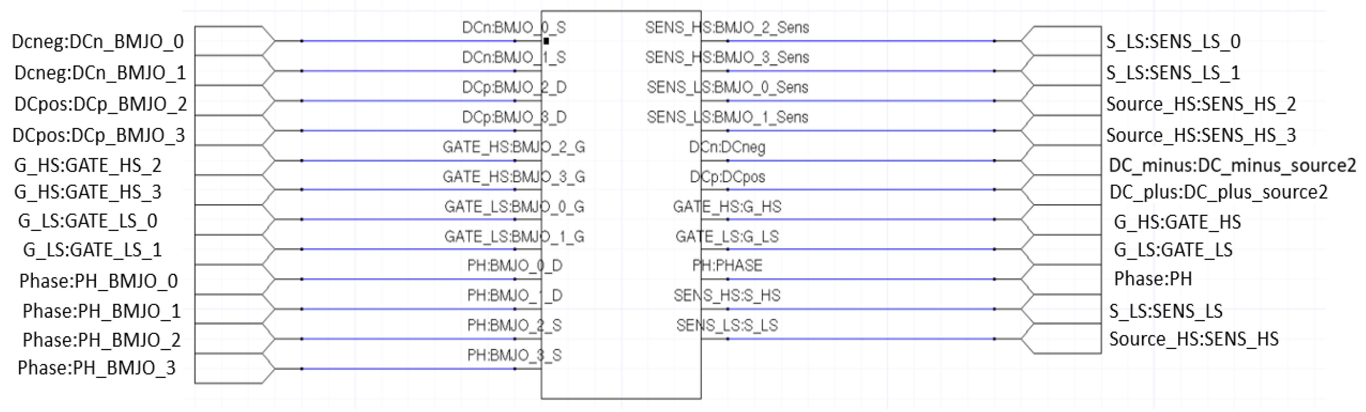
3.1. Description of the System

The system belongs to the category of automotive applications designed for the HEV market. It is a zero-voltage switching (ZVS) converter featured by a DC/DC converter block at the battery side (Figure 4).
Resonant converters in their half-bridge implementation are increasingly popular in front-end DC/DC converters thanks to their interesting characteristics such as high efficiency, low switching noise, and the ability to achieve high power density. A potential drawback of these converters derives from their quite high (for this class of applications) switching frequency that can cause high dv/dt on internal nodes, affecting EMI performance [29].
There are many topologies of resonant converters that can be grouped according to the number of resonant elements. Among the most well-known topologies (LLC, CLL, and LCL), this paper focuses on an LLC configuration as reported in Figure 5.
Power switches M1 and M2, which, in our case study, were SiC MOSFETs (breakdown voltage 1200 V, conduction resistance 21 mΩ, rated current 91 A), were configured to form a square-wave generator. This generator produced a unipolar square-wave voltage, V s q , by driving switches Q1 and Q2, with alternating 50% of the duty cycles for each switch. A small amount of dead time is needed to prevent the possibility of cross-conduction and to allow time for ZVS to be achieved.
The resonant circuit consisted of the resonant capacitance, C r , and two inductances, the series resonant inductance, L r , and the transformer’s magnetizing inductance, L m . The transformer turn ratio was n. The resonant network circulates the electric current and, as a result, the energy is circulated and delivered to the load through the transformer.
On the converter’s secondary side, two diodes constitute a full-wave rectifier to convert AC input into DC output and supply load R L . The output capacitor smooths the rectified voltage and current. The rectifier network can be implemented as a full-wave bridge or centre-tapped configuration with a capacitive output filter [30].
Figure 6 shows an overview of LLC converter operation and waveforms.
The device under test (DUT) is the IPEM reported in Figure 1, which is the core of the half-bridge square-wave generator block whose simplified top-view diagram is reported in Figure 7.
The equivalent electric circuit is reported in Figure 8. The high slopes of the SiC MOSFETs current can generate overvoltage due to the presence of parasitic inductances of interconnections that may exceed the breakdown of the device. Moreover, the energy exchange between the parasitic inductances and the parasitic capacitance of both the board and the SiC MOSFET causes electromagnetic compatibility issues.
As reported in the introduction of this paper, the final objective of the work is the definition of an effective electromagnetic simulation flow tailored to IPEM specifications and based on a simulation platform distributed on circuit simulators and finite element method (FEM) tools that are able to predict its EMI radiative behaviour.
Figure 9 shows the previously proposed diagram that was applied to the case study.

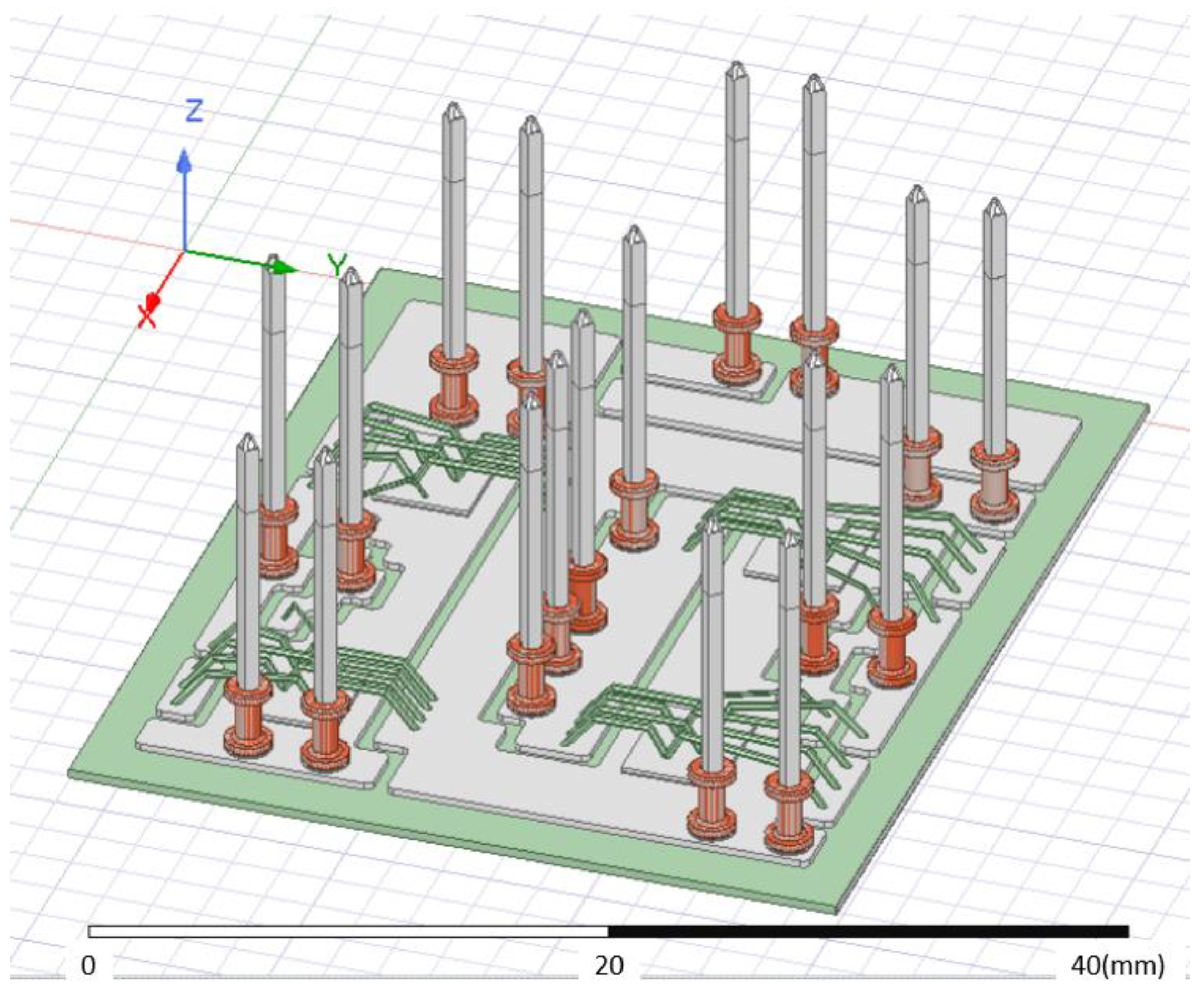
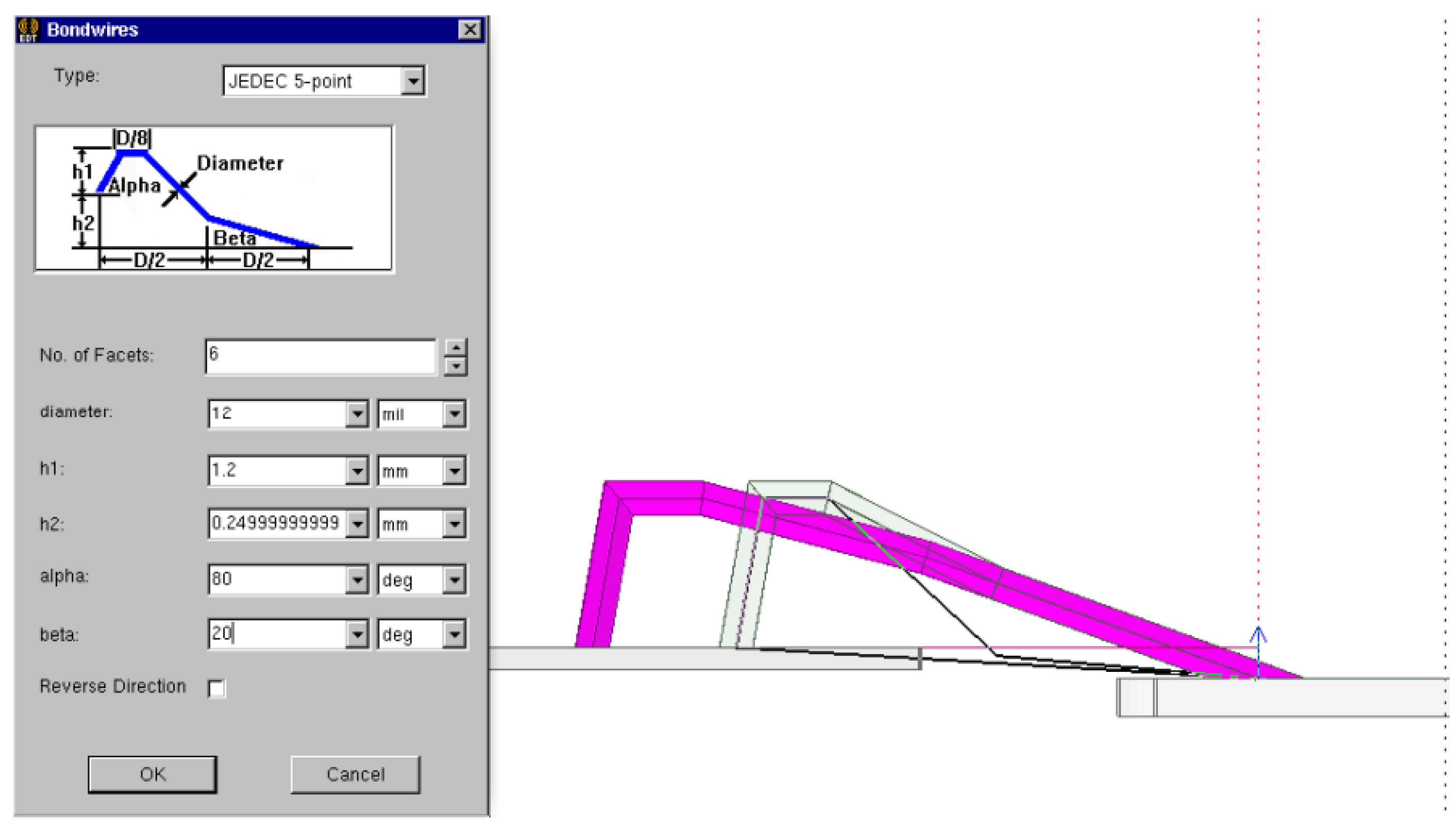
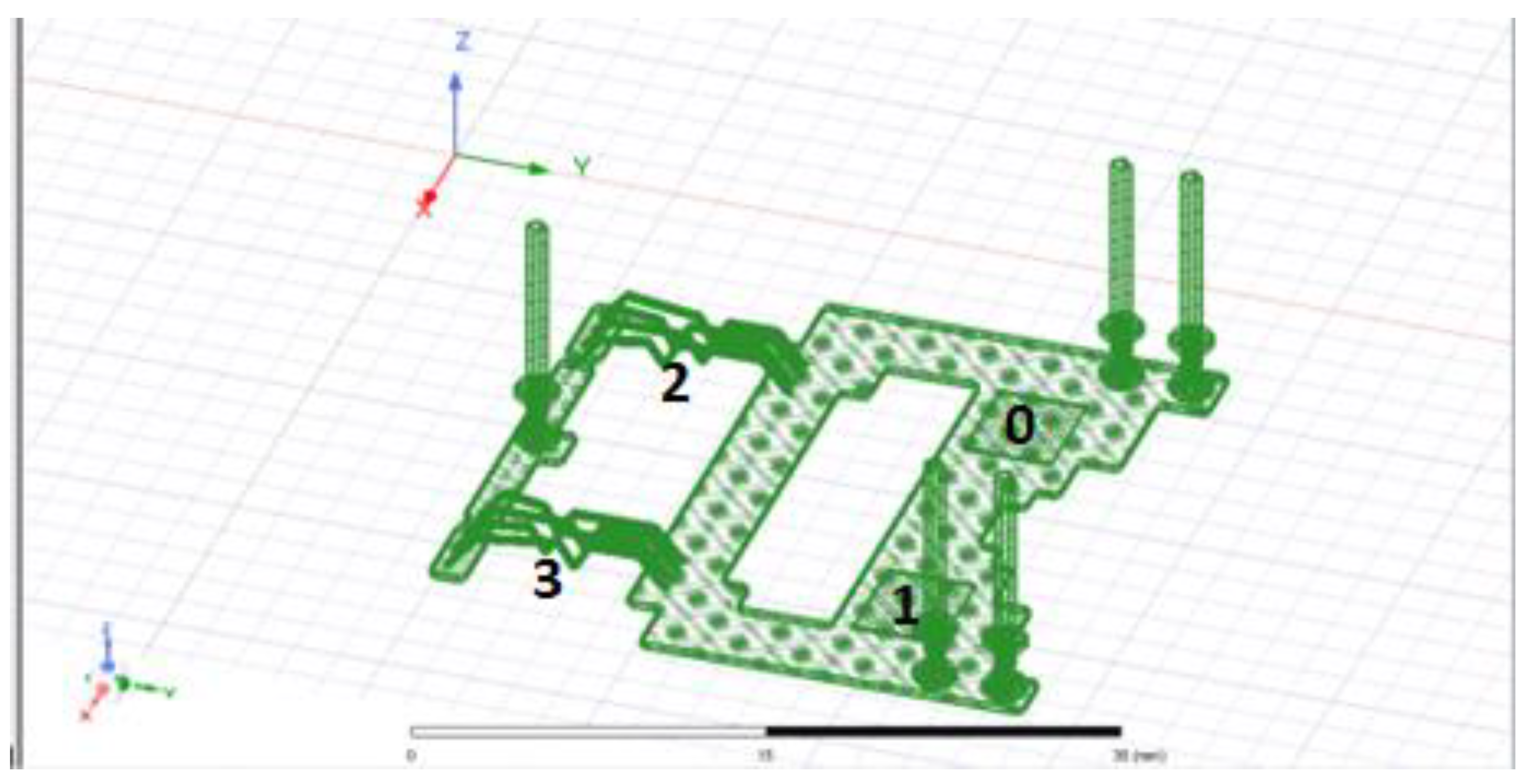
3.2. 3D DUT Model Generation

The first step is the generation of the 3D model of the IPEM structure as shown in Figure 1. The model was derived from a 2D AutoCAD-like representation of the DUT (Figure 7) by an extrusion process where several details of the package were accurately considered, such as bond wires and pins (Figure 10). This modelling phase was performed within the modeler of Ansys Q3D Extractor.
In detail, the diameter of the source and sense wires was 12 mils, and the diameter of the gate wires was 7 mils. After the interconnections had been implemented, we concluded the realisation of the 3D model of the power module by placing the pins in order to obtain the structure shown in Figure 11.
The definition of materials stack is an important aspect to which to pay attention. Materials can be assigned to 3D objects from some built-in CAD libraries; name, origin, relative permittivity, relative permeability, bulk conductivity, and tangent dielectric loss were considered for each material (Table 1).

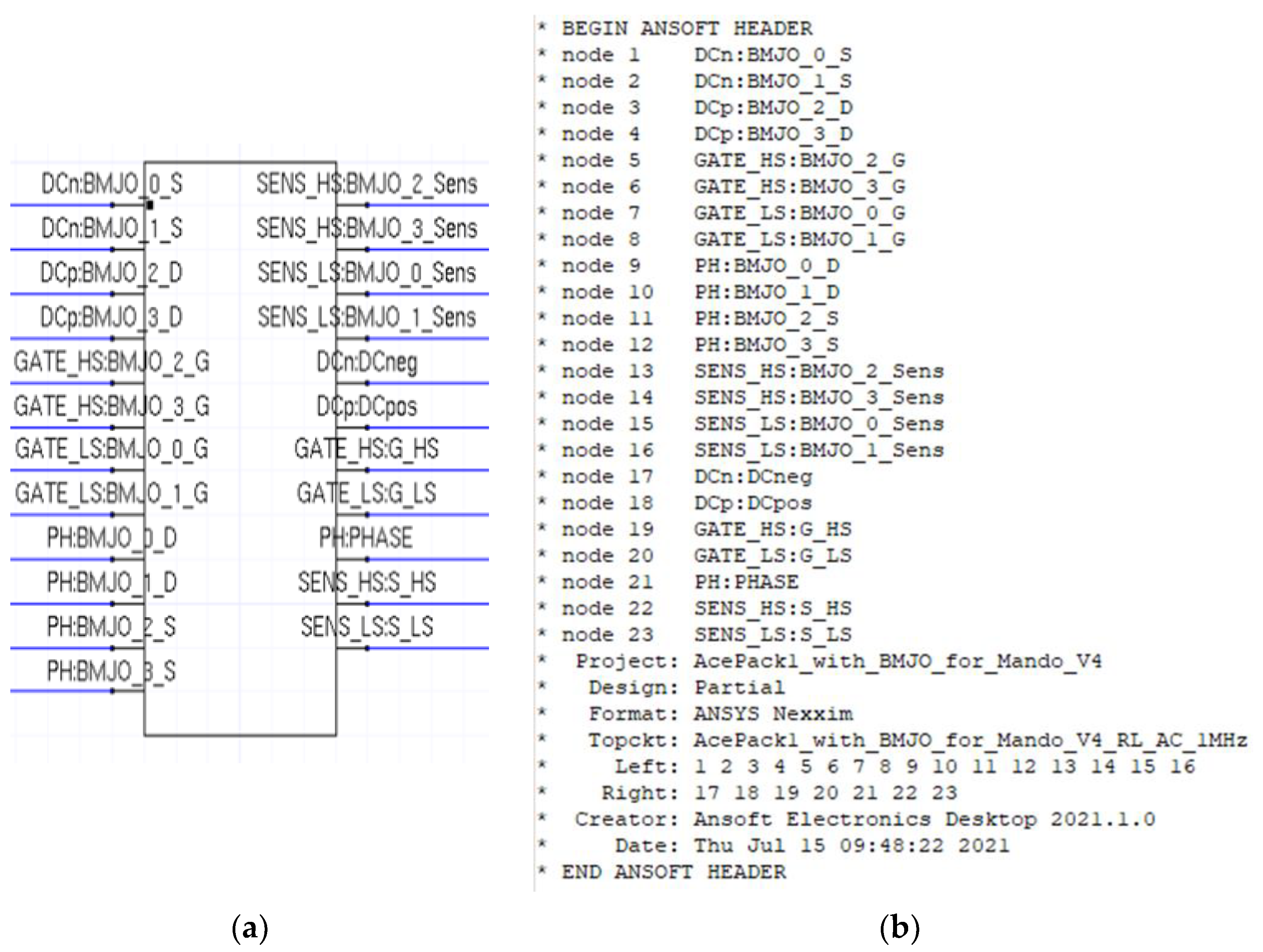
3.3. RLC Parasitic Extraction

In order to obtain simulation waveforms similar to real ones, it was necessary to combine accurate models of the SiC MOSFETs with the parasitic contributions. To this aim, RLC parasitic contributions were evaluated by means of the tool Ansys Q3D Extractor. This tool takes advantage of a surface mesh to calculate the high-frequency behaviour of conductive structures. It enables the efficient extraction of frequency-dependent partial inductances, resistances, and capacitive couplings between conductive nets, where a net is a collection of touching conductor objects separated by non-conducting materials or by the background material. The tool estimates these partial inductances within a power module and then provides an equivalent circuit representing the electromagnetic behaviour of the 3D modelling structure in a defined frequency range [31]. It is worth noticing that the simulation of the whole system (ideal components plus parasitic contributions) could pose some challenges in terms of simulation convergence and computational burden. A potential solution to this problem is the use of a single-frequency RLC matrix extracted at 1 MHz.
The result of this step is the extraction of a lumped RLC netlist encapsulated in the matrix shown in Figure 12.

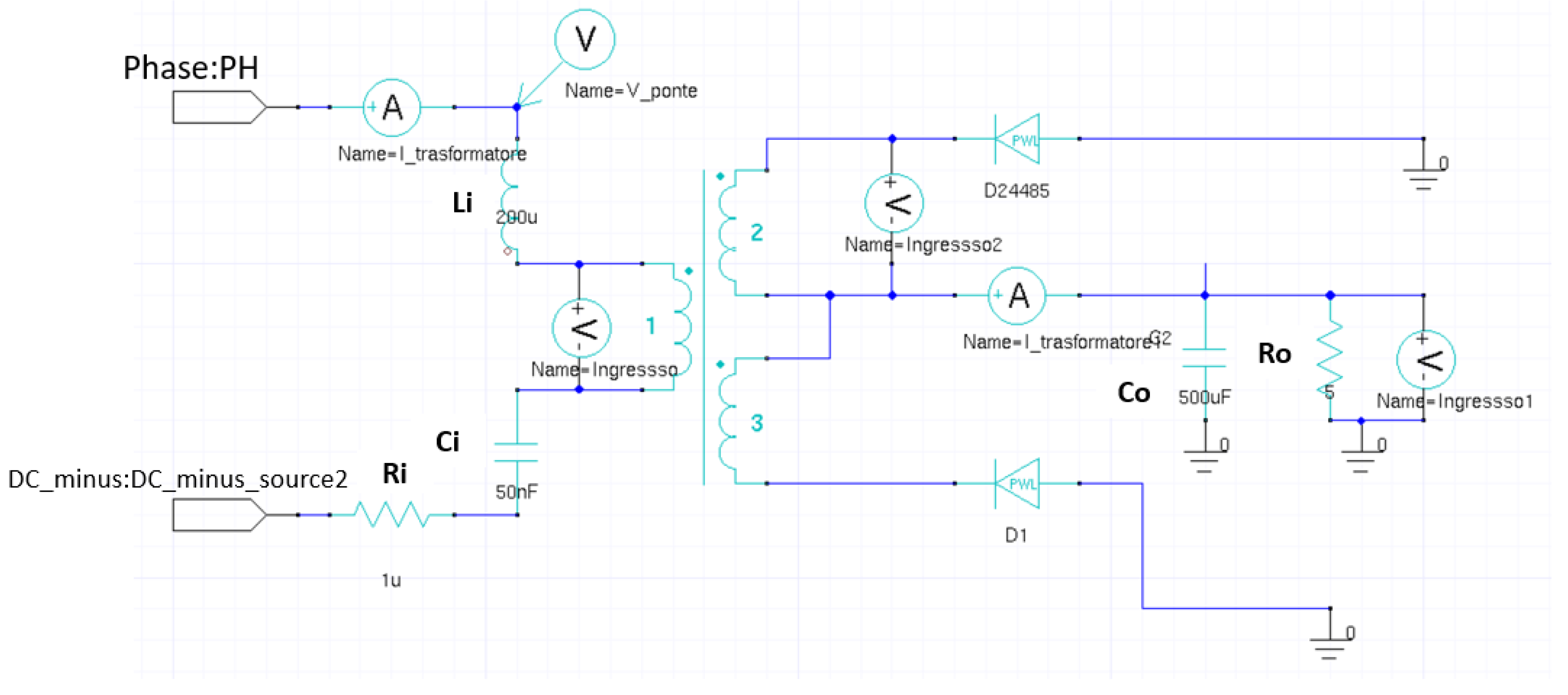
3.4. SPICE Simulation Accounting for Parasitic Components

The objective of the circuit simulation is to obtain voltage spectra on the converter nets to be used as excitations for the final radiative simulation. For this purpose, the test bench shown in Figure 13, Figure 14 and Figure 15 was set up.
The test bench comprised the RLC matrix, two SiC devices in parallel, components of the LLC converter (Figure 16), and a stimulus. The simulation was conducted with the Ansys Circuit Design Simulator. Table 2 reports the main quantities related to the LLC converter, and the simulations were carried out considering an ideal transformer.

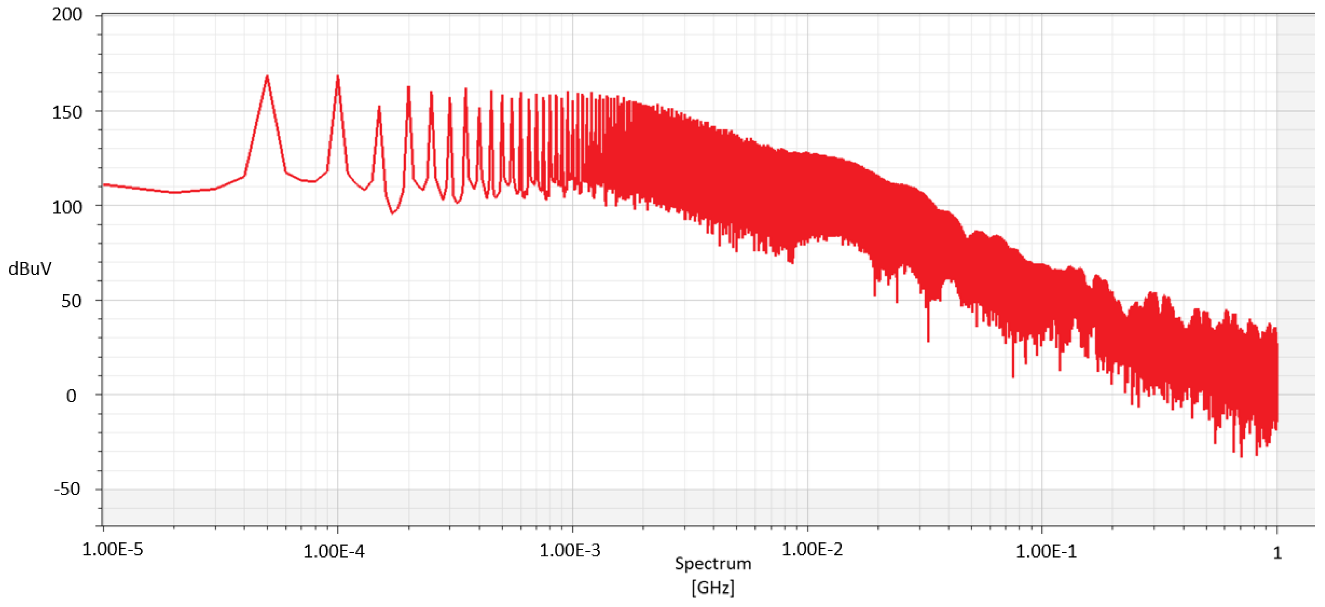
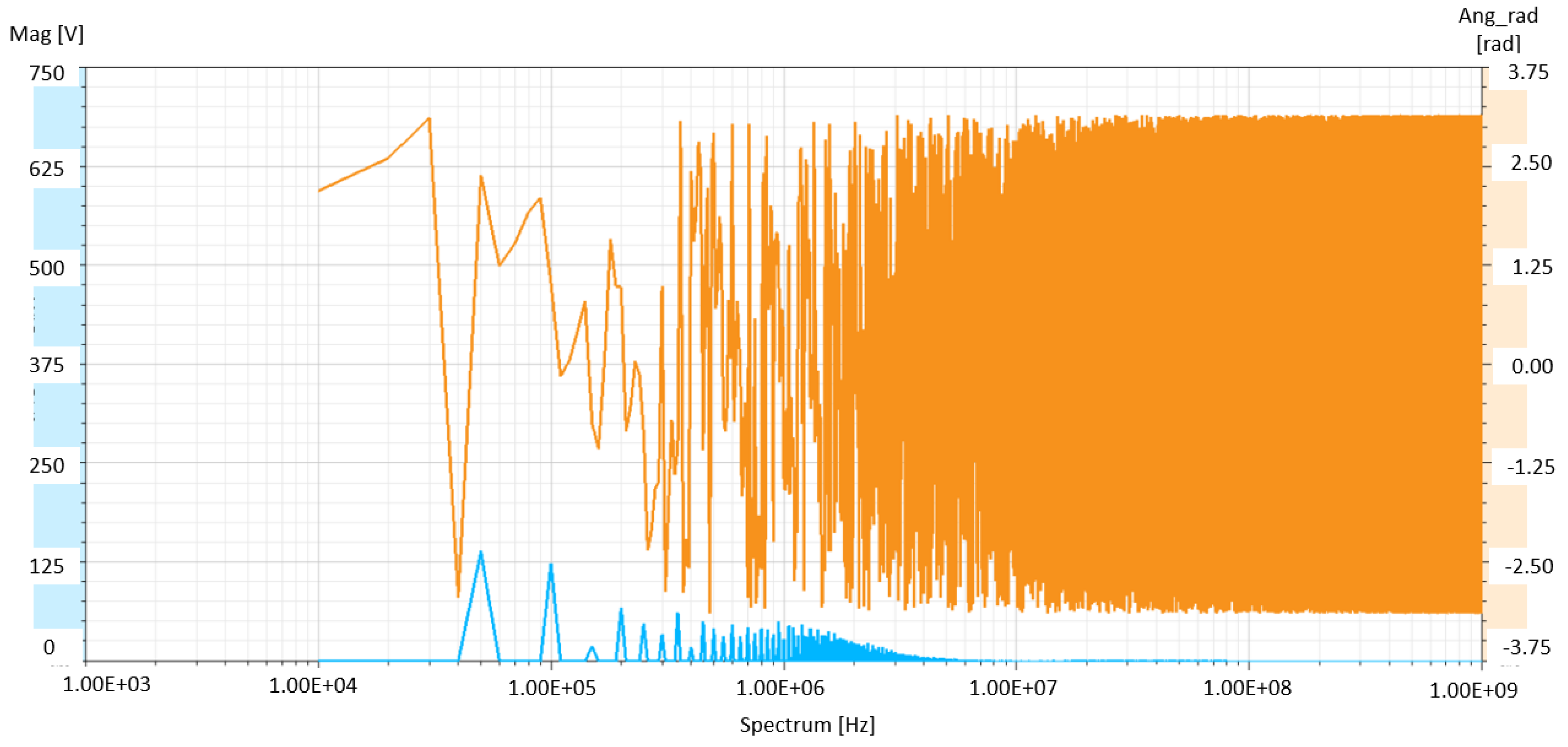
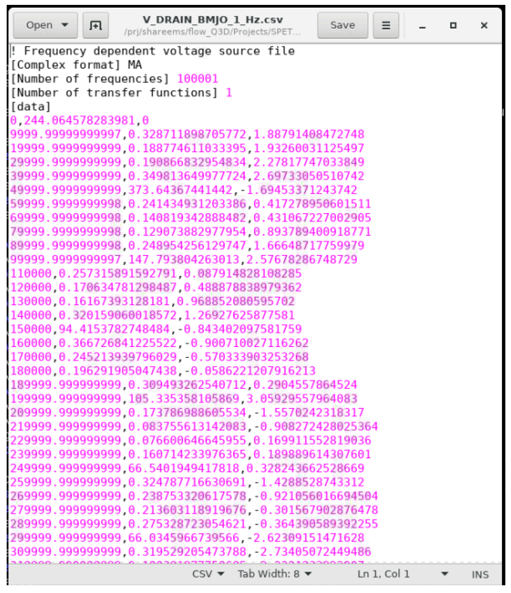
3.5. Spectral Extraction on Nets

Once the transient simulation had been finished, the spectra related to the voltage of the nodes were obtained. Figure 17 depicts the PHASE net. For each net, it was necessary to assign N “source” ports and only one “sink” port. Figure 18 reports one spectrum from 0 to 1 GHz of the PHASE net. Specifically, the PHASE NET depicted in Figure 17 was the net that connected the LLC converter to the ideal transformer.
All the spectra related to the remaining nets were derived and then converted into a proper format (magnitude/phase) (Figure 19) to be pushed as excitations to 3D FEM Solver Ansys HFSS. The final step consisted of converting waveforms data into a numerical table as shown in Figure 20.

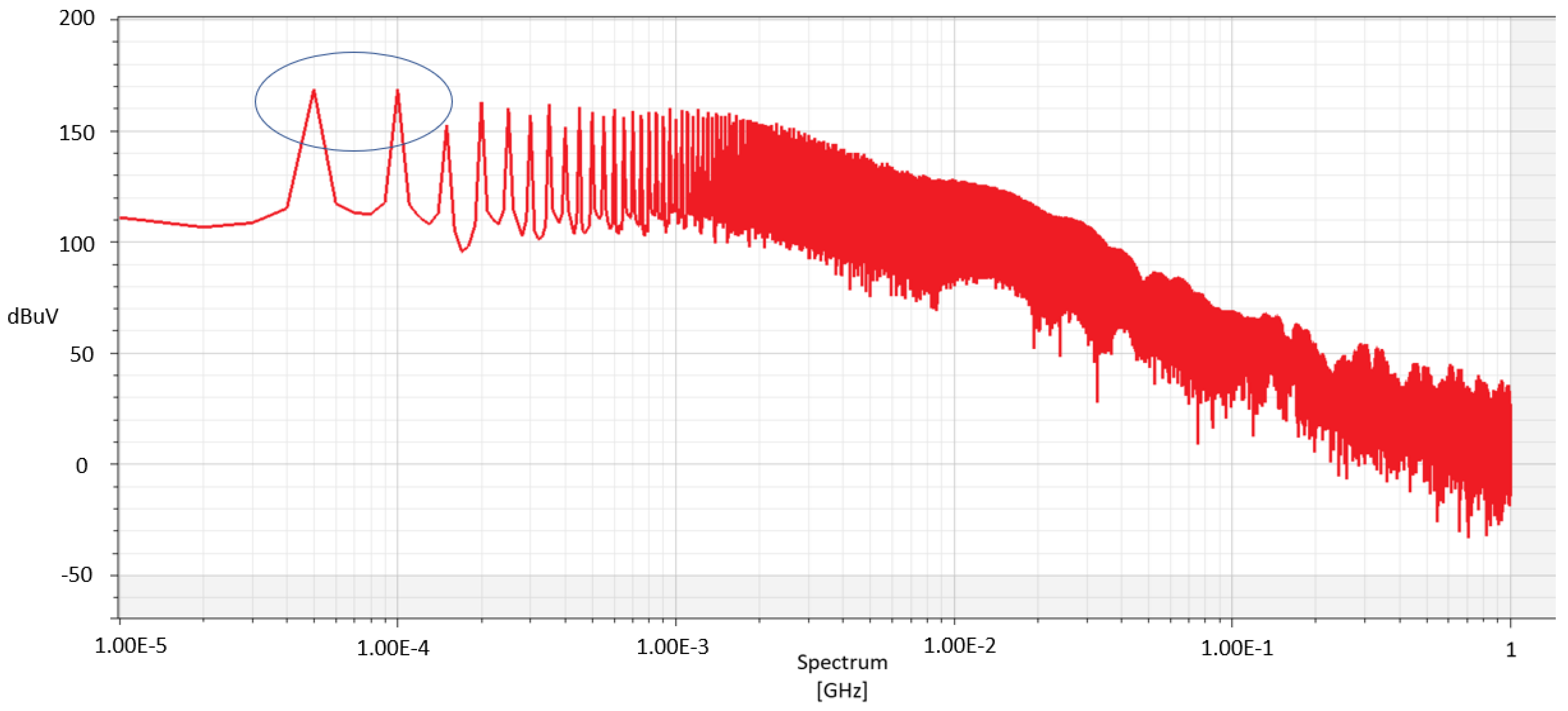
3.6. 3D FEM Radiative Simulation

Before performing the radiative simulation, some steps were necessary. First, it was necessary to import the Q3D DUT model into the 3D solver Ansys HFSS. This operation was conducted quite smoothly since the two tools belong to the same simulation suite. The only action to complete the excitation flow was the need to assign special ports at the points of interest of the 3D model. Second, it was also necessary to define the boundary conditions that specified the field behaviour at the edges of the system region and object interfaces. Boundaries in HFSS exist for two main purposes; the first is to create either an open or a closed model. “Open” represents a structure where energy cannot escape except through an applied port, for example, a waveguide; “closed” represents an electromagnetic model that allows for electromagnetic energy to be radiated away. Examples can be a PCB, an antenna, or any structure that is not enclosed within a closed cavity. The second reason why boundaries are used within HFSS is to define a smaller computational domain and decrease the geometric or electromagnetic complexity of a given structure or model.
In our case, we focus our attention on the radiation boundary (Figure 21) that is used to create an open model in HFSS, and the boundaries were placed a quarter wavelength away from any radiating surface.
One of the most interesting features of the proposed flow is the possibility to directly push spectra inside the 3D solver. Once the 3D structure is defined into HFSS, a dynamic link between the circuit simulator and HFSS must be established (Figure 22).
This operation involves the definition of some voltage sources associated with the aforementioned extracted spectra (numerical tables). These voltage sources were then used as excitations for the “dynamic-link” HFSS model. In order to obtain the advantage of the described “dynamic link” (interaction between “circuit designer” and HFSS), the system exploited the results of an HFSS simulation that had to be coupled with all excitations generated by the SPICE simulation. In this case study, the HFSS simulation was performed with the following parameters.
  • Frequency sweep: linear step.
  • Start: 10 kHz.
  • Stop: 1 GHz.
  • Step: 10 kHz.
Then, HFSS evaluates the electric field at each specified frequency, including the start and stop frequencies. After that, the HFSS simulation was completed, and the final electric field at 1 m can easily be plotted, as shown in Figure 23. Through such a plot, it was possible to foresee if the system was compliant with current regulations of the specific application field (e.g., CISPR), and thus to decide if the prototyping stage could start or if some changes were necessary for the system design.
An issue that arose at this step was the computational cost due to the high number of exciting nets (17). It is important to highlight that the HFSS simulation was limited to 30 Mhz to resolve this problem. In the specific case, the final HFSS simulation (in the range of 0–30 Mhz) lasted about 7 days by exploiting 8 medium-performance CPUs with an amount of memory of 800 Gb.

4. Conclusions

The definition of a simulation flow capable of estimating radiated EMI in power modules is an enabling tool to reduce them by optimal design. The need for measurements and/or the estimation of the EMI source without radiated EMI evaluation and/or the prediction of radiated EMI only due to the cables were the main limits of previous approaches.
Therefore, a workflow that combines circuit and electromagnetic simulations to evaluate the radiated emission of an integrated power electronics module, was defined and described. The key advantage of the proposed approach is the independence from experimental measurements at each assessment step, thus enabling considerable cost and time savings. In fact, it is not necessary to have a prototype and to perform anechoic chamber characterisation in order to estimate the emissions of the designed system. In other words, the strength of such a workflow is the ability to foresee the EMI of industrial products before realising the prototype, thus allowing for companies to save time and reduce the investment effort. This target was reached by the interaction and integration of the simulation results obtained from different simulation tools.
This work is a first step towards the development of a well-suited technique supporting an optimal design focusing on the reduction in radiated EMI. From this perspective, some noticeable aspects emerged from the workflow analysis in an actual case study. In detail, the discrete frequency sweep required considerable computational effort. This is indeed a critical aspect since it could significantly impact the overall activity timeline. For this reason, future developments of this work will focus on finding the best compromise between computational effort and estimation accuracy, and eventually devising new strategies for computational cost reduction with a limited effect on the simulation results’ accuracy.

Author Contributions

Conceptualization, G.G. and G.S.; Data curation, G.M.; Formal analysis, G.M.; Investigation, G.M., G.V. and S.A.R.; Methodology, G.G. and N.S.; Project administration, G.S.; Resources, G.S.; Software, G.M., G.V. and N.S.; Supervision, S.A.R. and N.S.; Validation, G.V.; Writing—original draft, G.M., G.G. and S.A.R. All authors have read and agreed to the published version of the manuscript.

Funding

The work has been supported in part by the project “Advanced power-trains and systems for full electric aircrafts—2017MS9F49” funded by the “Ministero dell’Università e della Ricerca” under the call PRIN 2017.

Conflicts of Interest

The authors declare no conflict of interest.

References

  1. Tran, H.; Segond, G. Modeling and analysis of EMI and overvoltage phenomenon in SiC inverter driven motor at high switching frequency. In Proceedings of the IEEE 18th International Power Electronics and Motion Control Conference (PEMC), Budapest, Hungary, 26–30 August 2018. [Google Scholar]
  2. Fink, S.; Hoffman, K.F.; Dickmann, S. Determining crucial sources of conducted interference in power electronics from heat sink capacitive coupling. In Proceedings of the International Symposium on Electromagnetic Compatibility—EMC EUROPE, Barcelona, Spain, 2–6 September 2019. [Google Scholar]
  3. Greco, G.; Vinci, G.; Raciti, A.; Cristaldi, G. Generation of electro-thermal models of integrated power electronics modules using a novel synthesis technique. In Proceedings of the IEEE 19th International Workshop on Thermal Investigations of ICs and Systems (THERMINIC), Berlin, Germany, 25–27 December 2013. [Google Scholar]
  4. Radchenko, A.; Khilkevich, V.; Bondarenko, N.; Pommerenke, D.; Gonser, M.; Hansen, J.; Keller, C. Transfer function method for predicting the emissions in a -cispr 25 test-setup. IEEE Trans. Electromagn. Compat. 2014, 56, 894–902. [Google Scholar] [CrossRef]
  5. Jia, J.; Rinas, D.; Frei, S. Predicting the radiated Emissions of Automotive systems according to CISPR 25 using current scan methods. IEEE Trans. Electromagn. Compat. 2016, 58, 409–418. [Google Scholar] [CrossRef]
  6. Weng, H.; Beetner, D.G.; DuBroff, R.E. Prediction of radiated Emissions using near field measurements. IEEE Trans. Electromagn. Compat. 2011, 53, 891–899. [Google Scholar] [CrossRef]
  7. Jia, J.; Rinas, D.; Frei, S. An alternative method for measurements of radiated emissions according to CISPR 25. In Proceedings of the International Symposium on Electromagnetic Compatibility (EMC EUROPE), Brugge, Belgium, 2–6 September 2013. [Google Scholar]
  8. Silaghi, A.; Motateanu, A.; Relu, A.; De Sabata, A. Far field versus Near field measurement in Automotive environment. In Proceedings of the IEEE 24th International Symposium for Design and Technology in Electronic Packaging (SIITME), Iasi, Romania, 25–28 October 2018. [Google Scholar]
  9. Camarda, A.; Calvano, F.; Mazhar Khan, A.; Balbarani, M.; Montanari, P.; Grossi, D. Computer Aided Engineering for optimal EMC design of On-Board Battery Chargers. In Proceedings of the International Symposium on Electromagnetic Compatibility—EMC EUROPE, Rome, Italy, 23–25 September 2020. [Google Scholar]
  10. Rajagopal, N.; DiMarino, C.; DeBoi, B.; Lemmon, A.; Brovont, A. EMI Evaluation of a SiC MOSFET Module with Organic DBC Substrate. In IEEE Applied Power Electronics Conference and Exposition (APEC); IEEE: Piscataway, NJ, USA, 2021. [Google Scholar]
  11. Zainal, S.; Jenu, M.Z.M. Reduction of conducted emission noise using various power supply filters. In Proceedings of the Asia-Pacific Conference on Applied Electromagnetics APACE, Shah Alam, Malayasia, 12–14 August 2003. [Google Scholar]
  12. Farhadi, A.; Jalilian, A. Modeling and simulation of electromagnetic conducted emission due to power electronics converters. In Proceedings of the 2006 International Conference on Power Electronic, Drives and Energy Systems, New Delhi, India, 12–15 December 2006. [Google Scholar]
  13. Domurat-Linde, A.; Hoene, E. Investigation and PEEC based simulation of radiated emissions produced by power electronic converters. In Proceedings of the 2010 6th International Conference on Integrated Power Electronics Systems, Nuremberg, Germany, 16–18 March 2010; pp. 1–6. [Google Scholar]
  14. Zhang, B.; Wang, S. Radiated electromagnetic interference modeling for three phase motor drive systems with SiC power modules. In Proceedings of the 2021 IEEE Applied Power Electronics Conference and Exposition (APEC), Virtual, 14–17 June 2021; pp. 2243–2250. [Google Scholar]
  15. Zhu, R.; Liang, T.; Dinavahi, V.; Liang, G. Wideband Modeling of Power SiC mosfet Module and Conducted EMI Prediction of MVDC Railway Electrification System. IEEE Trans. Electromagn. Compat. 2020, 62, 2621–2633. [Google Scholar] [CrossRef]
  16. Zhao, W.J.; Wang, B.F.; Liu, E.X.; Park, H.B.; Park, H.H.; Song, E.; Li, E.P. An Effective and Efficient Approach for Radiated Emission Prediction Based on Amplitude-Only Near-Field Measurements. IEEE Trans. Electromagn. Compat. 2012, 54, 1186–1189. [Google Scholar] [CrossRef]
  17. Benyoubi, F.; Pichon, L.; Bensetti, M.; le Bihan, Y.; Feliachi, M. An Efficient Method for Modeling the Magnetic Field Emissions of Power Electronic Equipment From Magnetic Near Field Measurements. IEEE Trans. Electromagn. Compat. 2017, 59, 609–617. [Google Scholar] [CrossRef]
  18. Schneider, D.; Böttcher, M.; Schoch, B.; Hurst, S.; Tenbohlen, S.; Köhler, W. Transfer functions and current distribution algorithm for the calculation of radiated emissions of automotive components. In Proceedings of the 2013 International Symposium on Electromagnetic Compatibility, Denver, CO, USA, 5–9 August 2013; pp. 443–448. [Google Scholar]
  19. Schneider, D.; Böttcher, M.; Tenbohlen, S.; Köhler, W. Estimation of radiated emissions of an automotive HV-inverter in a distributed system. In Proceedings of the 2014 International Symposium on Electromagnetic Compatibility, Tokyo, Japan, 12–16 May 2014; pp. 457–460. [Google Scholar]
  20. Zhang, Y.; Wang, S.; Chu, Y. Predicting far-field radiation with the emission models of power converters. In Proceedings of the 2017 IEEE International Symposium on Electromagnetic Compatibility & Signal/Power Integrity (EMCSI), Washington, DC, USA, 7–11 August 2017; pp. 797–802. [Google Scholar]
  21. Wei, S.; Pan, Z.; Yang, J.; Du, P. A Fast Prediction Approach of Radiated Emissions From Closely-Spaced Bent Cables in Motor Driving System. IEEE Trans. Veh. Technol. 2022, 71, 6100–6109. [Google Scholar] [CrossRef]
  22. Laour, M.; Tahmi, R.; Vollaire, C. Modeling and Analysis of Conducted and Radiated Emissions Due to Common Mode Current of a Buck Converter. IEEE Trans. Electromagn. Compat. 2017, 59, 1260–1267. [Google Scholar] [CrossRef]
  23. Shinde, S.; Masuda, K.; Shen, G.; Patnaik, A.; Makharashvili, T.; Pommerenke, D.; Khilkevich, V. Radiated EMI Estimation From DC–DC Converters With Attached Cables Based on Terminal Equivalent Circuit Modeling. IEEE Trans. Electromagn. Compat. 2018, 60, 1769–1776. [Google Scholar] [CrossRef]
  24. M’barki, Z.; Rhazi, K.S.; Mejdoub, Y. A proposal of structure and control overcoming conducted electromagnetic interference in a buck converter. Int. J. Power Electron. Drive Syst. 2022, 13, 380–389. [Google Scholar] [CrossRef]
  25. Park, J.; Song, C.; Park, J.; Kweon, H.; Ahn, S.; Fan, J.; Kim, H. Modeling and analysis of high speed switching Buck Converter IC for conducted emission estimation. In Proceedings of the 2020 International Symposium on Electromagnetic Compatibility—EMC EUROPE, Virtual, 23–25 September 2020. [Google Scholar]
  26. Kumar, S.; Akin, B.; Gohil, G. EMI Performance of Active Neutral Point Clamped Phase Leg for Dual Active Bridge DC–DC Converter. IEEE Trans. Ind. Appl. 2021, 57, 6093–6104. [Google Scholar] [CrossRef]
  27. Ishibashi, N.; Manepalli, L.K.; Nath, D.; Nayak, B.P.; Kadam, S.; Gope, D. Black-Box DC-DC integrated circuit modeling towards design for EMC in automotive electronics. In Proceedings of the 2021 IEEE International Joint EMC/SI/PI and EMC Europe Symposium, Raleigh, NC, USA, 13 August 2021; pp. 810–814. [Google Scholar]
  28. Yao, J.; Wang, S.; Luo, Z. Modeling, Analysis, and Reduction of Radiated EMI Due to the Voltage Across Input and Output Cables in an Automotive Non-Isolated Power Converter. IEEE Trans. Power Electron. 2022, 37, 5455–5465. [Google Scholar] [CrossRef]
  29. Muttaqi, K.; Haque, M.E. Electromagnetic interference Generated from fast switching Power Electronic Devices. Int. J. Innov. Energy Syst. Power 2008, 3, 19–26. [Google Scholar]
  30. Huang, H. Designing an LLC Resonant Half-Bridge Power Converter. Tex. Instrum. 2010, 3, 2010–2011. [Google Scholar]
  31. Badstübner, I.K.; Stark, R.; Guacci, M.; Kolarb, J.W.; Grossner, U. Parasitic extraction procedures for SiC power modules. In Proceedings of the 10th International Conference on Integrated Power Electronics Systems (CIPS 2018), Stuttgart, Germany, 20–22 March 2018. [Google Scholar]
Figure 1. Internal view of an IPEM (ACEPACK, STMicroelectronics).
Electronics 11 02498 g001
Figure 2. Outline of the proposed EM simulation flow.
Electronics 11 02498 g002
Figure 3. Example of electrical spectrum extracted from an internal node of the system.
Electronics 11 02498 g003
Figure 4. Simplified block diagram of an EV charger.
Electronics 11 02498 g004
Figure 5. LLC resonant converter.
Electronics 11 02498 g005
Figure 6. LLC converter operation and waveforms.
Electronics 11 02498 g006
Figure 7. Top view of the IPEM half-bridge square-wave generator.
Electronics 11 02498 g007
Figure 8. Electric circuit of the IPEM.
Electronics 11 02498 g008
Figure 9. Diagram flow of modelling phase and EM-FEM simulation.
Electronics 11 02498 g009
Figure 10. Bond wire JDEC-5.
Electronics 11 02498 g010
Figure 11. 3D model of the power module: (a) bond wires; (b) pin.
Electronics 11 02498 g011
Figure 12. Lumped RLC netlist: (a) RLC matrix block and (b) related netlist.
Electronics 11 02498 g012
Figure 13. SPICE Simulation test bench. Device (a) high and (b) low side.
Electronics 11 02498 g013
Figure 14. SPICE Simulation test bench. (a) Drivers; (b) stimulus.
Electronics 11 02498 g014
Figure 15. RLC matrix of the SPICE simulation test bench.
Electronics 11 02498 g015
Figure 16. LLC converter (SPICE).
Electronics 11 02498 g016
Figure 17. PHASE net. The number indicates the position of each DIE.
Electronics 11 02498 g017
Figure 18. The spectrum of PHASE net (0–1 GHz).
Electronics 11 02498 g018
Figure 19. Spectral noise of PHASE net (blue, magnitude; orange, angle).
Electronics 11 02498 g019
Figure 20. Spectral noise of PHASE net in tabular format (magnitude and angle).
Electronics 11 02498 g020
Figure 21. Solution type: boundary condition (radiation).
Electronics 11 02498 g021
Figure 22. Dynamic-link HFSS and circuit designer simulator. (a) Block HFSS, (b) voltage sources, (c) load.
Electronics 11 02498 g022
Figure 23. Radiated emissions results: 150 kHz to 30 MHz (E field@1m, sphere, dBu).
Electronics 11 02498 g023
Table 1. Material details.
MaterialObjectRelative
Permittivity
Relative
Permeability
Bulk
Conductivity
Dielectric Loss Tangent
CopperTop Layer, Bottom Layer1 9.99911 × 10 1 58 × 10 6 Si/m0
AluminumBond wire11.000021 38 × 10 6 Si/m0
SolderDie Solder, Pin Solder11 7 × 10 6 Si/m0
Al 2 O 3 CeramicDielectric layer9.8100
CuSn6Pin11 9 × 10 6 Si/m0
Cu-DHPPin Holder1 9.9991 × 10 1 45 × 10 6 Si/m0
Table 2. Main quantities related to the LLC converter.
ComponentsValues
Ci50 nF
Li200 nH
Co50 nF
Ro5 ohm
Vo350 V
Io70 A
T338 K
Switching frequency50 kHz
Publisher’s Note: MDPI stays neutral with regard to jurisdictional claims in published maps and institutional affiliations.

