1. Introduction
Approximate computing is a cutting-edge model that emphasizes performance as a design requirement, allowing researchers to sacrifice accuracy in the results, favoring increased power, latency, energy, and area. In the pursuit of better computing efficiency, approximate computing is presently used in data analytics, neuromorphic computing, circuit realization of deep learning models for artificial intelligence and machine learning, memory structures for multi-core processors, low-power FPGA, and ultra-low-power electronic design of devices. As with existing digital very-large-scale integrated (VLSI) design, a practical system must consistently deliver precise measurements. The development of energy-efficient strategies has been a primary driving force for chip designers to discover modern approaches to address these targets.
Approximate computing is motivated primarily by error-tolerant (ET) applications. Error tolerance refers to a system’s ability to accept outputs, although few of its basic operations are performed with a software or hardware approximation. A high error tolerance level is required in various applications, encompassing scientific computing, computer vision, statistical analytics, image and video analysis, and communication systems. All these technologies are resource-intensive, yet they have built-in error tolerance. In this context, approximate computing could be a solid choice for enhancing the software’s functionality by compromising accuracy in favor of computational performance.
In terms of power and performance, perfect accuracy comes at a significant price. A dramatic reduction in the correctness criterion can considerably reduce the design expense. Incorporating errors into the approximation design serves as the basis for approximate computation, which accelerates and enhances the device’s performance. A significant reduction in the hardware overhead due to the errors introduced compromises the accuracy for enhanced power, delay, and area.
Three key breakthroughs in data processing have fueled research into ET architecture: the advent of new computational paradigms, modifications in fabrication techniques, and variations in the diversity of applications. The gap between CMOS technology scaling capabilities and future application workload demands is steadily widening. Scaling CMOS technologies to optimize systems’ performance is no longer as cost-effective as it once was. Power, delay, and area minimization have become vital requirements for VLSI circuits as integration density has evolved. Error tolerance refers to the use of circuitry that is incorrect. While executing specific applications, it sometimes causes errors but offers good performance to end users. The associated increase in effective efficiency, and hence lower price parts, is the motive for adopting such techniques.
Throughout the previous decade, various studies have investigated approximate computing at the hardware and software levels of abstraction. Hardware methods adjust designs at the device abstraction level, while software methods bypass algorithm-level operations. At the hardware abstraction level, the majority of work in the approximation computing paradigm was conducted on arithmetic modules. Furthermore, adders have attracted the most attention regarding approximate computing among arithmetic units. Across all digital systems, delay and power are two mutually exclusive design characteristics, implying that strengthening one usually necessitates compromising the other. In the case of adders, nevertheless, the scenario is more acute. One approach to addressing this is to use approximate adders, sacrificing precision for delay and power.
The growing demand for massive data handling and a rapid response necessitates large, powerful adders, making it unsuitable for larger adders. The fundamental building component, the adder, is frequently the decisive factor in system performance. The adders used in conventional computational units include ripple carry adder (RCA), carry look ahead adder (CLA), carry skip adder (CSKA), carry save adder (CSA), carry select adder (CSLA), and parallel prefix adders. Various power reduction techniques have also been proposed and developed. There often exists a trade-off between speed, area, and power. This challenge may have a solution in ET adders. ET adders can significantly improve power consumption and performance by sacrificing accuracy.
This work proposes three ET adders that optimize power and delay while keeping the error within limits. The presented ET adder architectures are more apt for image blending applications. The structure of the paper is arranged in the following order: the literature review on some of the state-of-the-art approximate adders is discussed in
Section 2.
Section 3 describes the ET adders’ proposed design, methodology, and implementation details using Verilog HDL. The results and discussion, comprising the performance metric evaluation and error metric calculation of the proposed ET adders and existing approximate adders, is covered in
Section 4. The simulation results to demonstrate the efficiency of the proposed ET adders using the image blending application with respect to the existing approximate adders are also analyzed and discussed in
Section 4.
Section 5 delves into this paper’s conclusions.
2. Literature Review
An approximation adder is, in essence, a basic arithmetic unit that is primarily engaged in many ET applications to reduce resource utilization, and it has attracted much interest from research studies. There has been considerable work in approximate computing, which is reviewed and discussed in this section. Zhu et al. [
1] suggested the design of an approximate adder that attains considerable savings in power and speed. In their design, accurate adders were introduced to add higher-order bits to preserve the correctness of the result. The power and delay were significantly reduced by the simultaneous addition of the accurate and inaccurate parts. An ASIC implementation of the proposed ET adders was carried out by provisioning the custom design of the inaccurate part of the adder.
In their research, Priyadharshni et al. [
2] described an imprecise full adder (IFA) that was utilized to develop two 16-bit error-tolerant adders (ETA). The first ETA was designed by utilizing the modified full and half adders for the lower inaccurate portion. The MSB portion of the adder was designed using a power-optimized CSLA. The proposed adders demonstrated significant power and area reductions over the previous approximate adders.
The design of a 1-bit modified full adder (MFA) by Geetha et al. [
3] eliminated carry propagation by tolerating errors in the carry bit. The authors constructed a 16-bit high-speed ETA (HSETA) using the proposed MFA for lower-order bits and the standard CSLA for upper-order bits. They assessed the efficiency of HSETA in terms of accuracy, gate count, delay, and power consumption, compared with that of contemporary adders. Although there was a significant reduction in delay, the power savings were not considerable.
Thus far, the presented designs have been less explored in practical image/signal processing applications. The research that deals with the application of image processing in approximate computing is discussed here to analyze the impact of the processed image’s peak-signal-to-noise ratio (PSNR). The researchers Gnanambikai et al. [
4] presented a parallel adder with optimum accuracy utilizing approximate computing. The carry select technique for addition was merged with the carry bypass strategy for the design’s signal and image processing applications. Image blending was used to test the functionality of the proposed designs. The proposed technique demonstrated enhanced accuracy and lower power than the standard CSLA system.
Jothin et al. [
5] investigated, in their work, the performance of a Significance Approximation ET CSLA (SAET-CSLA) for image processing applications. The hardware complexity was minimized by using an algorithmic strength reduction method, thereby reducing the power. In their work, Jothin et al. [
6] emphasized inexact applications using the image blending operation by examining the newly proposed High-Performance ETA (HPETA). Significant benefits were observed due to the reduction in the critical path delay and gate-level logic. Switching activity and carry propagation delay were lowered using a multiplexer to determine the sum based on pre-computation, resulting in faster speeds and less area. As an extension of their work, Jothin et al. [
7] proposed a carry select approximate full adder designed for high performance by introducing only one error. These adders were targeted mainly towards 8-bit image processing applications of high accuracy.
Dutt et al. [
8] reported the implementation of four approximate full adders in the context of energy efficiency and high-performance computing by employing image processing applications. The research added new dimensions by reducing the carry propagation distance while maintaining a low error rate. The study found that integrating the carry lifetime with error correction and detection logic improved the error rate.
Priyadharshni et al. [
9] examined two types of approximate adders, both of which utilized Boolean logic approximation to minimize hardware complexity while retaining a substantial error rate tolerance. The evaluation of the proposed adders using the image blending application exhibited that it was suitable for error-resilient applications and showed improved NED, MED, and MRED values. Seo et al. [
10] found that adopting a hybrid error minimization technique in approximate adders resulted in computation accuracy and energy efficiency. Accurate adders such as RCA and CLA were utilized to obtain the precise segment of the resultant sum.
A few studies researched the influence of the Binary to Excess 1 Converter (BEC) in the CSLA to understand its impact on power and delay, and the findings are summarized below. Vaithiyanathan et al. [
11] devised a CSLA architecture based on BEC and a decider unit. The proposed 16-bit CSLA comprised CLAs with a size of 4 bits, along with the decider units. The undesirable switching of the BEC was eliminated by the introduction of the decider unit, resulting in overall optimization in area, power, and speed. Basant et al. [
12] developed a novel effective design for CSLA by optimizing the logic units in a logic formulation. Based on a Boolean logic analysis, the redundant activities in the standard and BEC-based CSLA were recognized and discarded. The proposed design used less space, and the delay was lower than in previous designs. Ramkumar et al. [
13] presented a design modification at the gate level to reduce the size and power of SQRT CSLAs. The proposed design exhibited lower area and power with a slightly larger delay than the standard CSLAs.
Ramkumar et al. [
14] employed a design by modifying CSA utilizing a BEC, making it more efficient with lower carry propagation latency. Though this proposed design was better than the standard design, it resulted in higher power dissipation and area. Minho et al. [
15] demonstrated and investigated, in their work, the implementation of a CSLA that substituted the RCAs of the standard design with high-speed and energy-efficient combinational logic.
The gate-level implementation of power-efficient and fast designs of CLAs and CSLAs was presented by Balasubramanian et al. [
16] using approximate and accurate computations to assess and evaluate the performance metrics. Their work also focused on the design and performance metric evaluation of hybrid CLAs and CSAs by incorporating BEC. The 32-bit adders implemented using hybrid RCLA and RCA in the accurate part showed lower values of energy delay product (EDP) and power delay product (PDP) in comparison to adders realized using CSLAs or CLAs. Balasubramanian et al. [
17] proposed a reduced-error approximation adder using improved hardware. In their work, Ahmad et al. [
18] designed two approximate adders with reduced errors by using the FPGA resources. Although approximation computing may be accomplished in all aspects of the computer, from software to circuits, the primary focus of this research will be on ET adders [
19,
20,
21,
22,
23,
24,
25]. Most of the work related to CSLA [
2,
3,
4,
5,
6] was devoted to developing the approximation hardware and minimizing the area and power. In higher-bit adders, the propagation delay problem becomes significant in CSLA due to the presence of the RCAs and multiplexers, which is overcome by introducing modifications at the architectural level. To reduce the carry propagation delay of the CSLA, CSKAs and CLAs [
16] are used in the upper-order bits of the proposed design, instead of the RCAs, which incurs a slightly larger area. The modified CSLA architecture with the newly proposed selector block used in the proposed work reduces the area and hence the power.
The construction of the newly proposed ET adders utilizing the Boolean expressions exhibited a considerable reduction in gate count and carry and sum delay. This research introduces three base ET adders apt for ASIC realizations and evaluates them in comparison to previous approximate adders. The novelty of the proposed design is the incorporation of the precomputation-based selector along with the BEC in the proposed ET-based CSLA adders, which minimizes the switching activity, thereby reducing the delay, area, and power while keeping the error as low as possible. The performance evaluation of the proposed ET adders is extended by the inclusion of RCA, CLA, and CSKA in the 16-bit proposed CSLAs to form nine variants. These nine designs are additionally employed in an image blending operation to understand the efficiency of the proposed ET adders.
3. Methodology
RCAs, CSLA, CLA, CSKA, and CSA are different fast adders implemented in the prevailing research. Across all adders, CSLA continues to be one of the quickest with area and power overhead. The CSLA’s basic concept includes two sections of RCAs, one fueled with a “zero” input carry and another with a “one” input carry, resulting in parallel computation. Multiplexers are used to determine the appropriate value of both predefined sums when the RCA block’s input carry appears. The subsequent output carry is also identified and forwarded to the following carry select segment. Since the precomputation of the sum is performed presuming that the previous carry is “zero” and “one”, the CSLA is the fastest among many contemporary adders regarding its computational overhead. Although the approaches adopted to develop the existing CSLAs are area-efficient, there is room for improved power savings to enhance the overall system’s efficiency. A portion of the RCAs appears to be operational, leading to higher power dissipation and area. The use of approximate computation in the CSLA can significantly simplify the hardware explored in this work.
Approximate computing [
1] can save a significant amount of power, delay, and area by sacrificing the accuracy of the outputs. The most important aspect of designing an approximate circuit is keeping the device and propagation delay to a minimum. A few incorrect results are allowed in complex designs to minimize the Boolean expressions and logic counts.
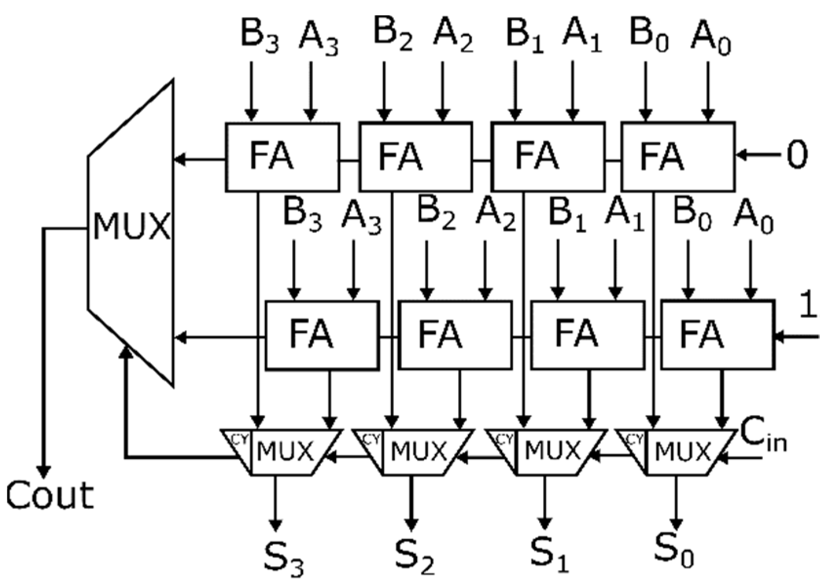
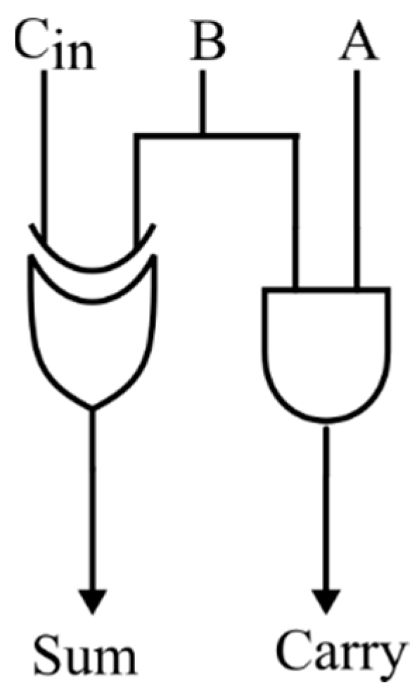
In conventional CSLAs, the sum bit is calculated concurrently for a carry input of 1 and 0 using the RCAs, as shown in
Figure 1, regardless of the previous carry. Depending upon the previous carry, the multiplexer decides the output. The RCA of size 4 bits, used in the conventional CSLA, will be functioning all the time, as shown in
Figure 1, and consists of four “OR”, eight “AND”, and eight “XOR” gates, resulting in increased area and power. In the proposed work, the selector unit replaces the RCAs in the conventional CSLA when the carry is one, as shown in
Figure 2, reducing the overall gate count and hardware complexity.
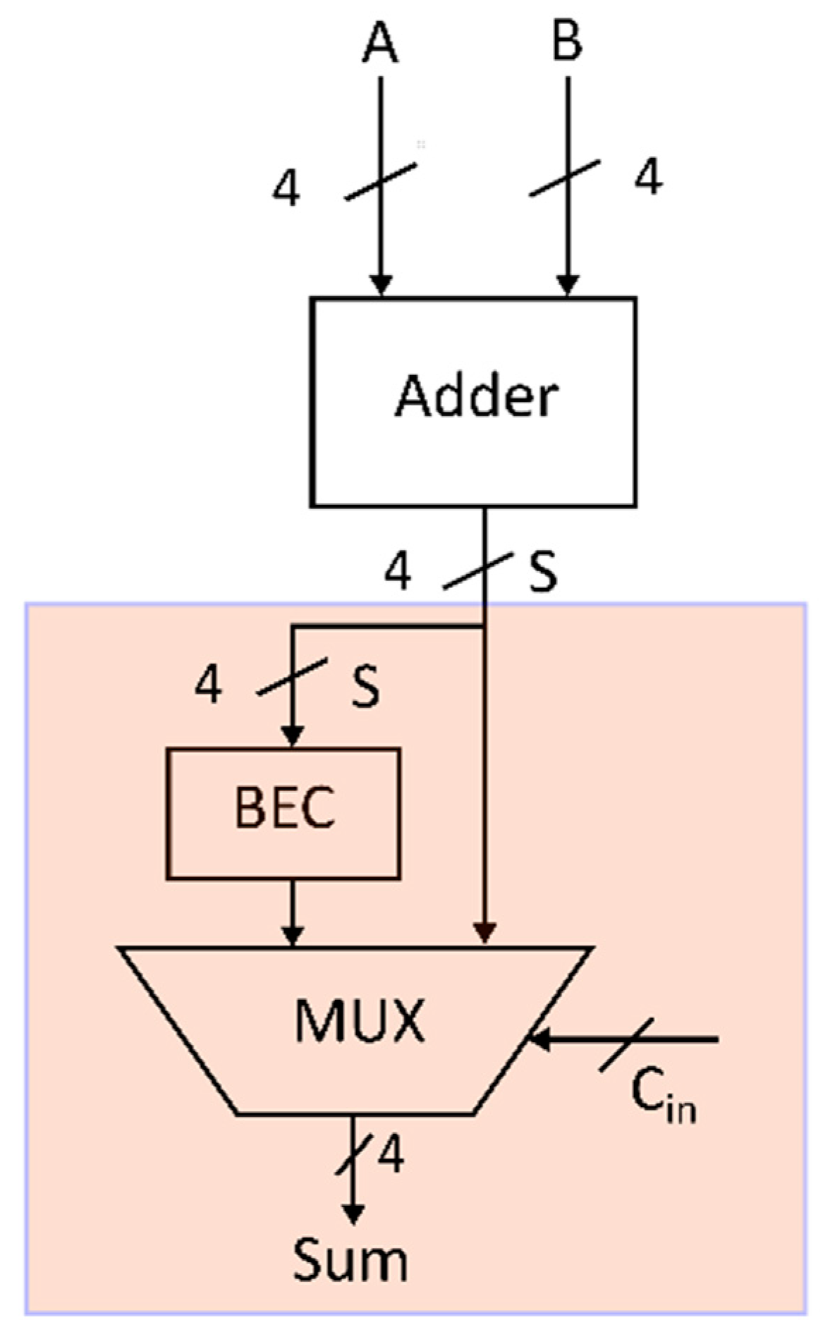
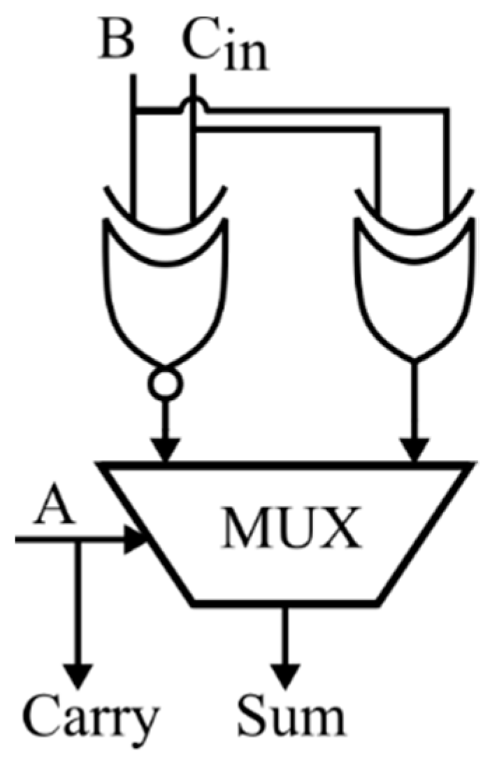
The proposed CSLA selects the sum output from A + B or (A + B) + 1 depending on the previous carry using the multiplexer, as illustrated in
Figure 2 above. An incrementor in the form of the BEC module is utilized here to realize (A + B) + 1 when the previous carry is one, instead of adding A + B twice. When the previous carry is zero, the sum from the proposed ETA is selected. When the previous carry is one, the sum generated from the BEC module is selected as the output. The carry-out passed to the next stage in the proposed CSLA is made dependent on the previous carry-in C
3. In this case, the extreme condition (corner case) when the inputs are A = 4′b0000, B = 4′b1111, C
in = 1′b0 may result in propagating an incorrect carry output of 1. This scenario is overcome by introducing an AND logic to pass the previous carry-in (C
3) to the OR gate. The “OR” operation between the carry generated from the proposed ETA (C
7) and the “AND” operation between the previous carry C
3 and the 5th bit of the BEC module (X
8) generates the carry-out that is propagated to the next stage. The equation for C
out is expressed as follows:
where
is the carry from A + B (proposed ETA),
is the carry from (A + B) + 1 (BEC module in this case), and
is the previous carry-in. The novelty of the adder is to design a selector block that selects the sum based on the carry from the previous stage and the AND-OR logic that selects the carry-out based on the previous carry-in.
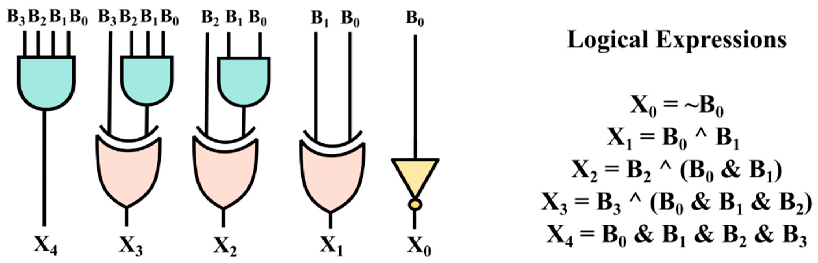
A bit in binary encoding has a value based on its position in the number. Excess 1 codes are unique because their value is +1 of their corresponding binary value. In [
12], a thorough analysis and application of BEC in CSLA was performed. The truth table for the BEC conversion is illustrated in
Table 1, which is used to obtain the logic expressions of the BEC module illustrated in
Figure 3. The carry bit/5th bit of the BEC module is obtained by the AND operation between the four binary bits, since the carry bit has to be set to one only when all the binary inputs are high. The logical expressions and the BEC module’s logic diagram are illustrated in
Figure 3. The BEC utilized in the proposed selector unit comprises three “XOR”, three “AND”, and one “NOT” gate, as illustrated in
Figure 3, lowering the area.
The selector unit replaces around half of the full adders used in the standard CSLA and the multiplexers, resulting in improved power and area optimization. Moreover, it is evident from
Table 1 that the transitions and functions associated depend only on one bit, further minimizing the power. These considerations reveal that the proposed selector unit occupies a substantially lower area and power than the 4-bit RCA. As a result, it is the most feasible alternative for the typical RCA-tuned adder. The proposed selector unit, which integrates the operations of the BEC and multiplexer, achieves area and power optimization.
As depicted in
Figure 4, the selector unit replaces the multiplexers and full adders used in the conventional CSLA illustrated in
Figure 1. The functionality of the selector block, as shown in the pseudocode, is to choose the output based on the carry input and to perform the BEC operation. The incorporation of the selector unit in the CSLA design and the proposed ET adders will minimize the operation of the BEC. The BEC switching activity appears to be mitigated when there is no carry generation, lowering the power and delay.
| Pseudocode: Selector Logic |
if (carry = 1)
sum = output from BEC
else
sum = output from adder
end |
3.1. Proposed One-Bit Error-Tolerant Full Adders
This paper proposes three base ET adder models: a selector-based error-tolerant adder (SBETA), a low-power selector-based error-tolerant adder (LPSBETA), and an optimized error-tolerant adder (OETA). The ET adders’ selector-based design minimizes the switching activity, lowering the area and power in the proposed approaches.
3.1.1. Selector-Based Error-Tolerant Adder (SBETA)
In the SBETA, a multiplexer-based design is introduced for the generation of carry, for which the decisive factor is the input “A” formulated by incorporating two 1-bit errors in the sum, as illustrated in
Table 2. The carry is defined by the “OR” operation between the “B” and “C
in” inputs, when the “A” input is zero. In cases when the “A” input is one, the “AND” operation between “B” and “C
in” inputs defines the carry output. The expression for the sum is reduced to the inversion operation of the carry generated. This reduces the gate count to 7, and the gate delay of the sum and carry is reduced to 4 and 3, respectively. The sum and carry expressions are presented in
Table 2.
Figure 5 illustrates the structure of the proposed SBETA design. The pseudocode for the sum and carry of LPSBETA is as given below.
| Pseudocode: SBETA unit |
if (A == 0)
Cout = B | Cin
else
Cout = B . Cin
end |
| sum = ~Cout |
The introduction of two errors in the carry instead of the sum is utilized in the second base design, LPSBETA, which is discussed in the next section.
3.1.2. Low-Power Selector-Based Error-Tolerant Adder (LPSBETA)
The LPSBETA employs a multiplexer to generate the sum output using “A” input as the selection input. In the carry of the LPSBETA, inducing two one-bit errors minimizes the Boolean expressions of the sum and carry, as can be seen in
Table 2. The introduction of the errors lowers the gate count to ten and eliminates the carry gate delay, while the sum gate delay is reduced to four.
Figure 6 illustrates the structure of the proposed LPSBETA design. The pseudocode for the sum and carry of LPSBETA is as given below. OETA is presented as the third base design to minimize the gate count and delay, thereby reducing the area.
| Pseudocode: LPSBETA unit |
if (A == 0)
sum = B ⊙ Cin
else
sum = B ⊕ Cin
end |
| Cout = A |
3.1.3. Optimized Error-Tolerant Adder (OETA)
As depicted in
Table 3, the OETA is constructed by introducing four errors in the sum and two errors in the carry to simplify the Boolean expressions and minimize the area. The gate count is lowered to four, and the sum and carry gate delay is reduced to two and one, respectively, due to the approximation introduced.
Figure 7 represents the architecture of the proposed OETA design.
| Pseudocode: OETA unit |
| sum = B ⊕ Cin |
| Cout = A . B |
The pseudocode for the sum and carry of OETA is as given above.
3.2. Proposed 16-Bit Error-Tolerant CSLAs
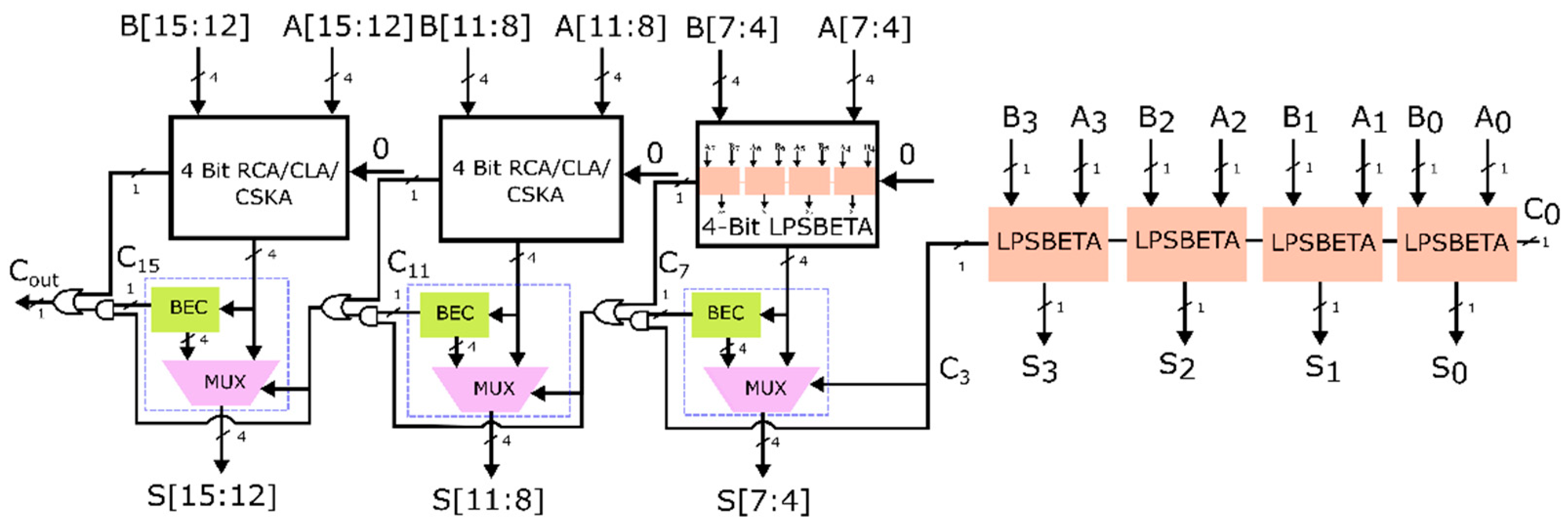
The construction of the 16-bit modified CSLA utilizing the proposed ET adders for the lower 8 bits and modified CSLA adders for the upper 8 bits is explored in this section to evaluate the performance of the proposed ET adders. Incorporating RCAs, CSLAs, and CSKAs in the upper 8 bits of the 16-bit CSLAs resulted in nine variants of ET adders with remarkable power and delay benefits, detailed here.
3.2.1. Design 1: Modified CSLA-Based SBETA Using RCA
The inaccurate lower 4-bit portion of the proposed design 1, the modified CSLA-based SBETA using RCA, uses the SBETA shown in
Figure 5. An improved version of CSLA incorporating a selector unit is employed for the next upper four bits. The selector unit is activated to compute the sum based on the carry generated in the preceding section.
The carry C
3 from the previous SBETA module selects the sum output S[7:4] using the multiplexer. The 4 one-bit SBETA adders with input A[7:4] and B[7:4] compute the sum assuming the carry input C
3 as 0, and this sum output is given to the BEC module. When carry C
3 is zero, the sum output from the 4 one-bit SBETA adders is selected as the output sum S[7:4]. The output of the BEC module is selected as the output sum when the carry C
3 is one. As the carry-out of each 4-bit block in the proposed CSLA depends on the previous carry-in, an AND-OR logic is introduced, as illustrated in
Figure 8. The carry-out to the next stage is generated by the “OR” operation between the carry generated from the proposed SBETA (C
7) and the AND operation between the previous carry (C
3) and the 5th bit of the BEC module.
The carry generated from the second stage selects the sum output S[11:8] from the next 4-bit RCA module when the carry is zero. When the carry is one, the output from the BEC module is selected as the output sum. The third-stage carry generated selects the sum output S[15:12] from the last 4-bit RCA module when the carry is zero. The BEC module output is selected as the sum output when the carry is one. The final carry Cout is generated by the OR operation between C15 and the AND operation between the previous carry and the 5th bit of the last BEC module.
When no carry is generated from the preceding stage, delay and power are minimized, eliminating the switching activity in the BEC.
Figure 8 depicts the proposed modified CSLA-based SBETA.
3.2.2. Design 2: Modified CSLA-Based LPSBETA Using RCA
LPSBETA is utilized for the proposed ETA’s lowest four bits. A modified version of CSLA incorporating the selector unit is used for the next upper four bits of the LPSBETA. The selector unit determines the sum based on the carry generated from the previous stage. LPSBETA is used for sum computation when the carry is zero. When the carry is zero, RCAs are used for the upper eight bits, whereas, when the carry is one, the BEC module output is selected by the selector unit. The proposed 16-bit CSLA-based LPSBETA, named Design 2, is illustrated in
Figure 9.
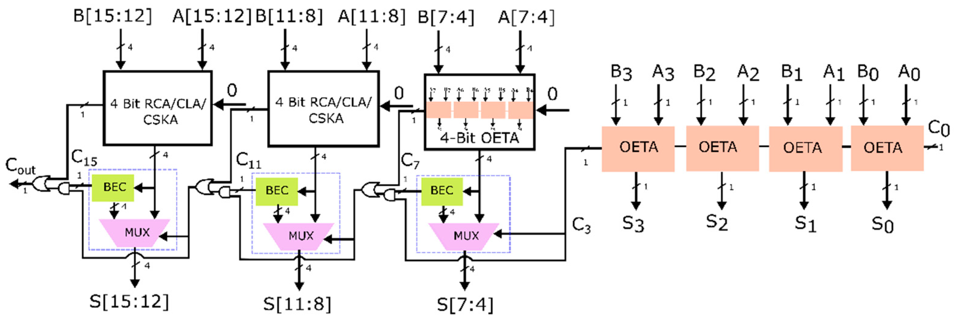
3.2.3. Design 3: Modified CSLA-Based OETA Using RCA
OETA is used to construct the lowest four bits of the proposed 16-bit CSLA-based OETA, Design 3. The conventional CSLA is modified by integrating the selector unit for the next higher four bits, when the carry generated from the preceding stage is one. When the carry is zero, OETA is utilized to generate the sum. When the carry is zero, RCAs are used for the upper eight bits, whereas, when the carry is one, the BEC module output is selected by the selector unit. The proposed 16-bit CSLA-based OETA, named Design 3, is illustrated in
Figure 10.
3.2.4. Extended Designs
The performance of the ET adders in Designs 1, 2, and 3 is assessed by replacing the RCAs in the upper 8 bits with CLAs and CSKAs. The incorporation of the CLAs and CSKAs in the proposed work helps to analyze the performance of the proposed ET adders. Despite their straightforward design, RCAs have a significant propagation delay constraint within the logic circuitry. As a result of this delay, the RCA is very slow. The CLA can help to resolve this disadvantage. Designs 4, 5, and 6 explore the reduction in propagation delay induced by the CLA’s faster addition logic to analyze the performance of the proposed ET adders. This is accomplished by replacing the 4-bit RCA with 4-bit CLA in Designs 1, 2, and 3. Since the CLA is more expensive and has a more complex architecture, which increases with the number of bits, the design of the CSLA is further modified by using a CSKA. The minimization of the critical path delay using the CSKA involves skipping the carry bit whenever the propagate signal is one, resulting in a faster design. To explore the effectiveness of CSKA using the proposed SBETA, LPSBETA, and OETA, the CSLA is modified by replacing the 4-bit RCA of Designs 1, 2, and 3 with CSKA to obtain Designs 7, 8, and 9.
The work is further extended by designing 32-bit CSLA-based ET adders in a similar fashion, where the lower 16 bits are designed using the proposed ET adders and the upper 16 bits are designed using accurate adders. Higher-order CSLA-based ET adders can be designed similarly.
4. Results and Discussion
This section evaluates and assesses the proposed ET adders and the approximate adder’s performance metrics in terms of power, area, and delay. The error metrics’ calculation is also explained. The demonstration of the image blending application to evaluate the efficiency of the proposed ET adders with respect to the existing approximate adders is also analyzed and discussed.
4.1. Proposed Error-Tolerant and Existing Approximate Adders’ Performance Metric Comparison
The performance of the prevailing 16-bit and 32-bit approximate adders and the proposed ET adders is analyzed using Verilog hardware description language (HDL), using 90 and 45 nm technology libraries. All of the designs are evaluated through the same framework, which examines the various parameters. The proposed ET adders and existing approximate adders’ functionality is analyzed using the actual and expected results. The proposed 16-bit and 32-bit ET adders and approximate adders’ performance attributes of delay, power, area, PDP, EDP, and area delay product (ADP) are presented in
Table 4 and
Table 5 and depicted in
Figure 11. The proposed designs indicate a reduction in delay, power, and area in comparison to the existing approximate adders, as shown in
Table 4.
The nine designs are categorized as Group I, II, and III to investigate the performance metrics of the proposed ET CSLAs. Group I comprises Designs 1, 4, and 7, constructed using SBETA; Group II includes Designs 2, 5, and 8, built with LPSBETA; and Group III consists of Designs 3, 6, and 9, formed with OETA. The inferences drawn from
Table 6 indicate that the average PDP of the Group I, II, and III 16-bit ET-based CSLA adders show savings of 34.45%, 40.7%, and 40.02% compared to the prevailing adder, EMFA [
6], when implemented using the 90 nm technology library. The average EDP shows a reduction of 46.44%, 57.24%, and 55.22% from EMFA [
6] for Group I, II, and III 16-bit ET-based CSLA adders, respectively, when implemented using the 90 nm technology library. Meanwhile, the ADP shows a reduction of 29.69%, 42.12%, and 35.07% from EMFA [
6] for Group I, II, and III 16-bit ET-based CSLA adders, respectively, using the 90 nm technology library.
The final inference of the proposed 16-bit ET adders implies that Design 1 attained the lowest power and Design 2 achieved the lowest area, delay, EDP, PDP, and ADP compared to the existing designs, making them suitable for power and area-efficient image processing applications. The percentage savings in PDP, EDP, and ADP of the 16-bit and 32-bit ET adders using 90 and 45 nm are summarized in
Table 6.
4.2. Accuracy Computation: Error Metrics
The reference metrics [
1,
26] are used and investigated in this section to demonstrate the feasibility of the ET adders proposed for ET implementations. In terms of measures such as normalized error distance (NED), mean error distance (MED), mean relative error (MRE), mean square error (MSE), mean absolute error (MAE), mean error (ME), and accuracy,
Table 7 illustrates the measured values for the existing and proposed 16-bit ET CSLAs. In MATLAB, an in-depth study of the error metrics was performed using 65,536 input vectors. When the inputs were random, and each input appeared only at a certain probability, the MED was applied. The arithmetic distance between the result from the actual adder and the ET adder is referred to as the error distance (ED), given by Equation (2).
Ra—represents the result from the actual adder;
Re—represents the result from the ET adder.
An architecture’s MED is the average of the EDs of all feasible outputs for each input. The ratio of MED to the maximum magnitude of the output of the accurate adder yields the NED. The mean relative error (MRE) is explored to analyze the accuracy of the proposed ET adders. The ratio of the ED to the output of an actual adder is termed the relative error (RE), given by Equation (3).
The proposed 16-bit ET CSLAs exhibited lower error metrics than existing approximate adders. As a result, they are more versatile for erroneous applications while necessitating less hardware overhead. To measure the average of the squares of errors, the MSE was calculated and analyzed using Equation (4).
where
= image generated from the accurate adder and
= image generated from the proposed ET adder.
The MAE is calculated using Equation (5) to analyze the absolute value of the mean error.
Equation (6) specifies adder accuracy (A) in terms of the inputs used in ET adders to depict the correctness of the adder result. Its percentage varies from 0% to 100%.
Minimum Allowable Precision (MAP): Even though some inaccuracies are permitted at an ETA’s output, the precision of a permissible output should be sufficient (more than a threshold value) to fit the system’s requirements. An acceptable result is when the minimal accuracy of an adder exceeds the minimum allowable precision.
Acceptance Probability (AP): The probability that an adder’s accuracy is greater than the minimum allowable precision is known as acceptance probability.
The inferences drawn from
Table 7 indicate that the average MED of the Group I adders was reduced by 99.95%, 99.93%, and 99.82% from FTFA [
4], ETCSLA [
5], and EMFA [
6], respectively. The average MED of Group II adders was reduced by 99.92%, 99.96%, and 92.56% from FTFA [
4], ETCSLA [
5], and EMFA [
6], respectively, whereas there was a reduction of 99.82%, 99.91%, and 81.97% in MED for Group III adders from FTFA [
4], ETCSLA [
5], and EMFA [
6], respectively. There was a reduction in MSE of 99.48%, 99.99%, and 99.47% from FTFA [
4], ETCSLA [
5], and EMFA [
6], respectively, for Group I adders. In the case of Group II adders, the MSE was reduced by 60.2%, 99.54%, and 99.41% from FTFA [
4], ETCSLA [
5], and EMFA [
6], respectively. There was a reduction in MSE of 48.97%, 99.41%, and 47.9% from FTFA [
4], ETCSLA [
5], and EMFA [
6], respectively, for Group III adders.
Table 7 indicates that the proposed ET adders’ MED, NED, MRE, MSE, MAE, and ME all dramatically decreased. The average accuracy of Group I adders improved by 10.54%, 78.91%, and 9.21% from FTFA [
4], ETCSLA [
5], and EMFA [
6], respectively, whereas there was an improvement of 8.13%, 76.2%, and 7.5% in accuracy for Group II adders from FTFA [
4], ETCSLA [
5], and EMFA [
6], respectively, and an improvement of 8.6%, 75.76%, and 7.29% in accuracy for Group III adders from FTFA [
4], ETCSLA [
5], and EMFA [
6], respectively. The error metrics for Group I and Group II adders designed with SBETA and LPSBETA were significantly reduced since the errors introduced were lower in these adders.
4.3. Image Metrics of Proposed Adders and Existing Approximate Adders
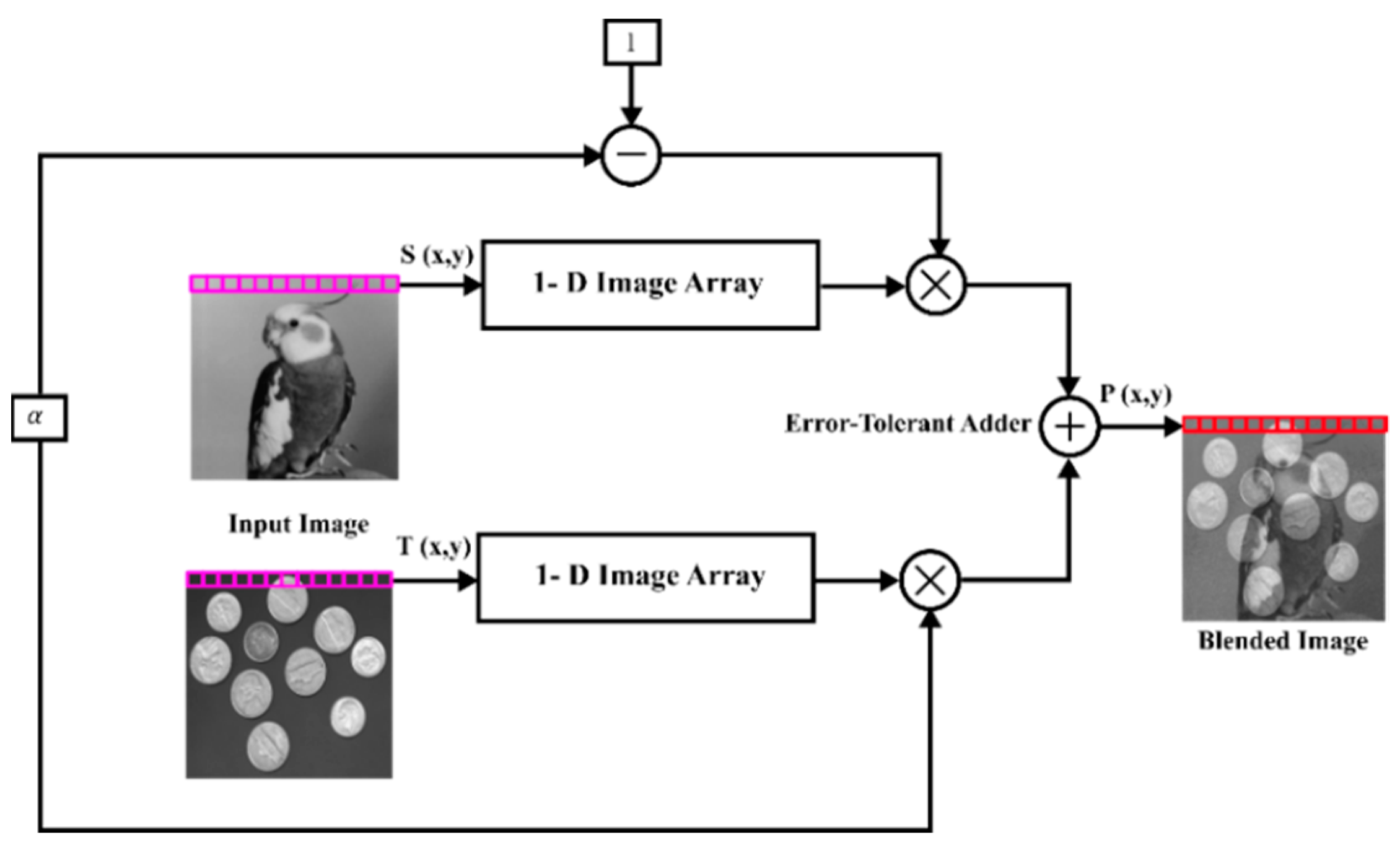
In this research, an image blending application is employed to validate the performance of the proposed ET adders. The operation of image blending is used to mathematically assess the correctness of the newly proposed ET adders and the existing approximate adders. Two images (S and T) are taken from a database of size 256 × 256 to investigate the image blending application. The algorithm for image blending is illustrated in
Figure 12 below and is coded using Verilog HDL. The two-dimensional images are transformed into a one-dimensional array. A blending factor of (1 − α) is multiplied with the first image and then added with the second image that is multiplied with α. The proposed ET adders and the existing approximate adders are used for the image blending addition algorithm to obtain the blended image. The 8-bit pixel values of the input images are transformed to 16-bit pixel values to execute 16-bit addition. The resultant blended image (P) is the linear summation of the input images’ pixels. The image blending operation is given by Equation (7).
where “α” is a blending factor for changing the foreground and background impact on the blended image’s contrast and brightness.
The PSNR is used to evaluate the performance of the proposed 16-bit ET adders and existing approximate adders [
27]. PSNR is calculated using the following Equation (8).
where Max is the maximum pixel value of the image. The value of Max is 255 as an 8-bit image is employed in this research. The equation to determine the mean squared error used in the denominator is given by Equation (4). The PSNR and MSE are inversely related to each other. A higher PSNR value implies that an image is of good quality. The PSNR value will be higher if the adder has fewer errors.
The overall working process of the image blending operation using the proposed ETAs is illustrated in
Figure 13 as follows:
MATLAB software reads the two digital input images and converts the image pixels to binary.
The binary value of the image pixels is transformed to text using MATLAB.
The image data are then retained in memory and read out using Verilog HDL for computation.
The proposed ET adders perform the image blending process implemented using Verilog HDL.
The blended image is written in text format and saved upon processing.
The text file is converted to the final blended image using the output file generated in MATLAB, and the output is evaluated.
Computation of the PSNR and MSE of the obtained image is used for image analysis.
The proposed ETA’s performance is evaluated using the Genus tool of Cadence, which calculates power, delay, and area.
The PSNR values of the output digital image of the proposed ET adders and the existing approximate adders are given in
Table 8. It is evident from
Table 8 that the proposed ET adders designed using SBETA have a higher PSNR than other existing 16-bit approximate adders. The analysis of the PSNR indicates that the adders designed using SBETA and LPSBETA are suitable for ET image processing applications.
The implementation and simulation of an image blending application in MATLAB to investigate the efficacy of the Group I, II, and III ET adders indicated that the designs proposed showed an improvement in PSNR of 64.89%, 49.84%, and 36.57% in comparison to EMFA [
6].
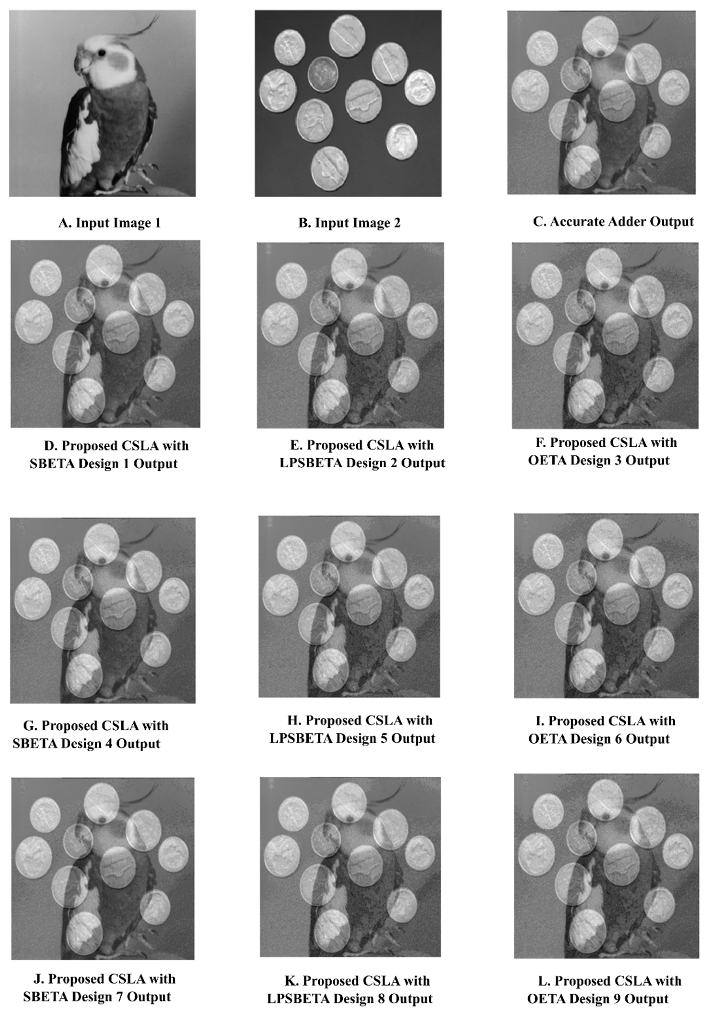
Figure 14A,B present the two digital input images and the output images (
Figure 14C–L) obtained after the image blending operation using the actual adder and the proposed ET CSLA-based adders for a blending factor of α = 0.5.
5. Conclusions
This article addressed the design of power and delay-optimized 16-bit and 32-bit CSLA-based ET, and its implementation using a 90 nm and 45 nm standard cell-based semi-custom application-specific integrated circuit design flow. The proposed ET adders were examined with existing 16-bit and 32-bit approximation adders using an image blending application to analyze and assess their efficiency and error metrics. The synthesis results showed significant power, area, and delay reductions, and lower error metrics. The proposed Design 1 exhibited the lowest power and highest PSNR, and Design 2 achieved the lowest area, delay, EDP, PDP, and ADP. Compared to the approximate adder designs, good accuracy in the computation of the proposed ET adders makes them suitable for power- and delay-efficient image processing applications. The future scope of work involves further development by including the proposed ET adders into convolution or digital filter applications involving addition.
Author Contributions
Conceptualization, T.M. and S.G.N.; methodology, T.M.; software, T.M.; investigation, T.M. and S.G.N.; resources, T.M. and S.G.N.; writing—original draft preparation, T.M.; writing—review and editing, V.K.P., V.S.R. and V.K.K.; supervision, S.G.N. All authors have read and agreed to the published version of the manuscript.
Funding
This research received no external funding.
Institutional Review Board Statement
Not applicable.
Informed Consent Statement
Not applicable.
Data Availability Statement
Not applicable.
Acknowledgments
The authors are thankful to Manipal Institute of Technology, Manipal Academy of Higher Education, for granting T.M.A. a Pai Fellowship to finish this study. The authors are also grateful to the Department of Electronics and Communication Engineering at Manipal Institute of Technology for providing the laboratory workspace. The authors would like to express their gratitude to Vikas R Bhat, Assistant Professor, MAHE, Manipal, for his valuable support.
Conflicts of Interest
The authors declare no conflict of interest.
References
- Zhu, N.; Goh, W.L.; Zhang, W.; Yeo, K.S.; Kong, Z.H. Design of low power high-speed truncation-error-tolerant adder and its application in digital signal processing. IEEE Trans. Very Large Scale Integr. (VLSI) Syst. 2010, 18, 1225–1229. [Google Scholar]
- Priyadharshni, M.; Kumaravel, S. Low power and area efficient error tolerant adder for image processing application. Int. J. Circuit Theory Appl. 2020, 48, 696–708. [Google Scholar] [CrossRef]
- Geetha, S.; Amritvalli, P. High Speed Error Tolerant Adder for Multimedia Applications. J. Electron. Test. Theory Appl. 2017, 33, 675–688. [Google Scholar] [CrossRef]
- Palanisamy, G.; Natarajan, V.K.; Sundaram, K. Area-efficient parallel adder with faithful approximation for image and signal processing applications. IET Image Process. 2019, 13, 2587–2594. [Google Scholar] [CrossRef]
- Jothin, R.; Vasanthanayaki, C. High Performance Significance Approximation Error Tolerance Adder for Image Processing Applications. J. Electron. Test. Theory Appl. 2016, 32, 377–383. [Google Scholar] [CrossRef]
- Jothin, R.; Vasanthanayaki, C. High performance error tolerant adders for image processing applications. IETE J. Res. 2018, 67, 205–216. [Google Scholar] [CrossRef]
- Jothin, R.; Vasanthanayaki, C. High Performance Four Segment Error Tolerant Adder for 8-bit Pixel Depth Image Processing Applications. J. Signal Process. Syst. 2020, 92, 693–703. [Google Scholar] [CrossRef]
- Dutt, S.; Nandi, S.; Trivedi, G. Analysis and Design of Adders for Approximate Computing. ACM Trans. Embed. Comp. Syst. 2017, 17, 1–28. [Google Scholar] [CrossRef]
- Priyadharshni, M.; Raj Gupta, A.; Nithish Kumar, V.; Kumaravel, S. An error efficient and low complexity approximate multi-bit adder for image processing applications. Int. J. Circuit Theory Appl. 2021, 49, 2373–2381. [Google Scholar] [CrossRef]
- Seo, H.; Yang, Y.S.; Kim, Y. Design and Analysis of an Approximate Adder with Hybrid Error Reduction. Electronics 2020, 9, 471. [Google Scholar] [CrossRef] [Green Version]
- Dhandapani, V. An Efficient Architecture for Carry Select Adder. World J. Eng. 2017, 14, 249–254. [Google Scholar] [CrossRef]
- Mohanty, B.K.; Patel, S.K. Area–Delay–Power Efficient Carry-Select Adder. IEEE Trans. Circuits Syst. II Express Briefs 2014, 61, 418–422. [Google Scholar] [CrossRef]
- Ramkumar, B.; Kittur, H.M. Low-power and area-efficient carry select adder. IEEE Trans. Very Large Scale Integr. (VLSI) Syst. 2012, 20, 371–375. [Google Scholar] [CrossRef]
- Ramkumar, B.; Kittur, H.M.; Kannan, P.M. ASIC implementation of modified faster carry save adder. Eur. J. Sci. Res. 2010, 42, 53–58. [Google Scholar]
- Nam, M.; Choi, Y.; Cho, K. High-speed and energy efficient carry select adder (CSLA) dominated by carry generation logic. Microelectron. J. 2018, 79, 70–78. [Google Scholar] [CrossRef]
- Balasubramanian, P.; Mastorakis, N. Performance Comparison of Carry-Lookahead and Carry-Select Adders Based on Accurate and Approximate Additions. Electronics 2018, 7, 369. [Google Scholar] [CrossRef] [Green Version]
- Balasubramanian, P.; Maskell, D.L. Hardware Optimized and Error Reduced Approximate Adder. Electronics 2019, 8, 1212. [Google Scholar] [CrossRef] [Green Version]
- Ahmad, W.; Ayrancioglu, B.; Hamzaoglu, I. Low Error Efficient Approximate Adders for FPGAs. IEEE Access 2021, 9, 117232–117243. [Google Scholar] [CrossRef]
- Kim, Y.; Zhang, Y.; Li, P. Energy Efficient Approximate Arithmetic for Error Resilient Neuromorphic Computing. IEEE Trans. Very Large Scale. Integr. (VLSI) Syst. 2015, 23, 2733–2737. [Google Scholar] [CrossRef]
- Mittal, S. A Survey of Techniques for Approximate Computing. ACM Comput. Surv. 2016, 48, 1–33. [Google Scholar] [CrossRef] [Green Version]
- Xu, Q.; Mytkowicz, T.; Kim, N.S. Approximate Computing: A Survey. IEEE Des. Test 2016, 33, 8–22. [Google Scholar] [CrossRef]
- Dalloo, A.; Najafi, A.; Garcia-Ortiz, A. Systematic Design of an Approximate Adder: The Optimized Lower Part Constant-OR Adder. IEEE Trans. Very Large Scale. Integr. (VLSI) Syst. 2018, 26, 1595–1599. [Google Scholar] [CrossRef]
- Jiang, H.; Liu, C.; Liu, L.; Lombardi, M.; Han, J. A Review, Classification, and Comparative Evaluation of Approximate Arithmetic Circuits. ACM J. Emerg. Technol. Comput. Syst. 2017, 13, 1–34. [Google Scholar] [CrossRef] [Green Version]
- Esmali Nojehdeh, M.; Altun, M. Systematic synthesis of approximate adders and multipliers with accurate error calculations. Integration 2020, 70, 99–107. [Google Scholar] [CrossRef]
- Gupta, V.; Mohapatra, D.; Raghunathan, A.; Roy, K. Low-power digital signal processing using approximate adders. IEEE Trans. Comput. Aided Des. Integr. Circuits Syst. 2013, 32, 124–137. [Google Scholar] [CrossRef]
- Mrazek, V.; Hrbacek, R.; Vasicek, Z.; Sekanina, L. Evoapprox8b: Library of approximate adders and multipliers for circuit design and benchmarking of approximation methods. In Proceedings of the Conference on Design, Automation & Test in Europe, Lausanne, Switzerland, 27–31 March 2017; pp. 258–261. [Google Scholar]
- Gonzalez, R.C.; Woods, R.E.; Masters, B.R. Digital Image Processing; Pearson International Edition: Bellingham, WA, USA, 2009. [Google Scholar]
Figure 1.
Conventional CSLA.
Figure 1.
Conventional CSLA.
Figure 3.
Binary to Excess 1 Converter (BEC) module.
Figure 3.
Binary to Excess 1 Converter (BEC) module.
Figure 4.
Selector unit of the proposed CSLA.
Figure 4.
Selector unit of the proposed CSLA.
Figure 5.
Proposed SBETA design.
Figure 5.
Proposed SBETA design.
Figure 6.
Proposed LPSBETA design.
Figure 6.
Proposed LPSBETA design.
Figure 7.
Proposed OETA design.
Figure 7.
Proposed OETA design.
Figure 8.
Design 1/4/7: Modified CSLA-based SBETA using RCA/CLA/CSKA.
Figure 8.
Design 1/4/7: Modified CSLA-based SBETA using RCA/CLA/CSKA.
Figure 9.
Design 2/5/8: Modified CSLA-based LPSBETA using RCA/CLA/CSKA.
Figure 9.
Design 2/5/8: Modified CSLA-based LPSBETA using RCA/CLA/CSKA.
Figure 10.
Design 3/6/9: Modified CSLA-based OETA using RCA/CLA/CSKA.
Figure 10.
Design 3/6/9: Modified CSLA-based OETA using RCA/CLA/CSKA.
Figure 11.
PDP—EDP plot for 16-bit proposed and existing ET adders.
Figure 11.
PDP—EDP plot for 16-bit proposed and existing ET adders.
Figure 12.
Image blending operation.
Figure 12.
Image blending operation.
Figure 13.
Architecture of image blending operation.
Figure 13.
Architecture of image blending operation.
Figure 14.
Image blending output for α = 0.5.
Figure 14.
Image blending output for α = 0.5.
Table 1.
Four-bit BEC truth table.
Table 1.
Four-bit BEC truth table.
| Binary | Excess 1 |
|---|
| 0000 | 00001 |
| 0001 | 00010 |
| 0010 | 00011 |
| 0011 | 00100 |
| 0100 | 00101 |
| 0101 | 00110 |
| 0110 | 00111 |
| 0111 | 01000 |
| 1000 | 01001 |
| 1001 | 01010 |
| 1010 | 01011 |
| 1011 | 01100 |
| 1100 | 01101 |
| 1101 | 01110 |
| 1110 | 01111 |
| 1111 | 10000 |
Table 2.
Proposed and existing approximate adders’ logical formulas and delay estimates.
Table 2.
Proposed and existing approximate adders’ logical formulas and delay estimates.
| Design | Sum Equation | Carry Equation | GDC 1 | GDS 2 | TGC 3 |
|---|
| SBETA | ~Cout | A?(B | Cin):(B.Cin) | 3 | 4 | 7 |
| LPSBETA | A?(B ⊙ Cin):(B ⊕ Cin) | A | 0 | 4 | 10 |
| OETA | B ⊕ Cin | A.B | 1 | 2 | 4 |
| Full Adder | A ⊕ B ⊕ Cin | ((A ⊕ B).Cin) | (A.B) | 2 | 2 | 9 |
| FTFA [4] | A ⊕ (B + Cin) | A + (B.Cin) | 2 | 3 | 6 |
| ET CSLA [5] | ~Cin | A.B + B.Cin + Cin.A | 4 | 1 | 6 |
| Approx. EMFA [6] | ~A.(B + Cin) + A(B.Cin) | A | 0 | 3 | 6 |
Table 3.
Proposed error-tolerant adders’ truth table (the symbol “✕” indicates the error introduced and “✓” represents no error).
Table 3.
Proposed error-tolerant adders’ truth table (the symbol “✕” indicates the error introduced and “✓” represents no error).
| Inputs | SBETA | LPSBETA | OETA |
|---|
| A | B | Cin | ES 1 | S | Cout | ED 3 | S | ECout 2 | Cout | ED | ES 1 | S | ECout | Cout | ED |
|---|
| 0 | 0 | 0 | 0 | 1 ✕ | 0 ✓ | +1 | 0 ✓ | 0 | 0 ✓ | 0 | 0 | 0 ✓ | 0 | 0 ✓ | 0 |
| 0 | 0 | 1 | 1 | 1 ✓ | 0 ✓ | 0 | 1 ✓ | 0 | 0 ✓ | 0 | 1 | 1 ✓ | 0 | 0 ✓ | 0 |
| 0 | 1 | 0 | 1 | 1 ✓ | 0 ✓ | 0 | 1 ✓ | 0 | 0 ✓ | 0 | 1 | 1 ✓ | 0 | 0 ✓ | 0 |
| 0 | 1 | 1 | 0 | 0 ✓ | 1 ✓ | 0 | 0 ✓ | 1 | 0 ✕ | −1 | 0 | 0 ✓ | 1 | 0 ✕ | −1 |
| 1 | 0 | 0 | 1 | 1 ✓ | 0 ✓ | 0 | 1 ✓ | 0 | 1 ✕ | +1 | 1 | 0 ✕ | 0 | 0 ✓ | −1 |
| 1 | 0 | 1 | 0 | 0 ✓ | 1 ✓ | 0 | 0 ✓ | 1 | 1 ✓ | 0 | 0 | 1 ✕ | 1 | 0 ✕ | −1 |
| 1 | 1 | 0 | 0 | 0 ✓ | 1 ✓ | 0 | 0 ✓ | 1 | 1 ✓ | 0 | 0 | 1 ✕ | 1 | 1 ✓ | +1 |
| 1 | 1 | 1 | 1 | 0 ✕ | 1 ✓ | −1 | 1 ✓ | 1 | 1 ✓ | 0 | 1 | 0 ✕ | 1 | 1 ✓ | −1 |
Table 4.
Analysis of performance metrics for proposed and existing 16-bit ET adders.
Table 4.
Analysis of performance metrics for proposed and existing 16-bit ET adders.
| SI. No: | 16-bit |
|---|
| Tech. Lib. | 90 nm | 45 nm |
|---|
| Design | Delay
(ns) | Power (µW) | Area (µm2) | PDP (fJ) | EDP
(e−21 Js) | ADP (µm2 ns) | Delay (ns) | Power (µW) | Area (µm2) | PDP (fJ) | EDP
(e−21 Js) | ADP (µm2 ns) |
|---|
| 1 | CSLA | 2.89 | 28.657 | 597.21 | 82.82 | 0.239 | 1725.94 | 4.18 | 25.369 | 326.73 | 106.04 | 0.443 | 1365.73 |
| 2 | FTFA [4] | 3.40 | 28.266 | 566.16 | 32.39 | 0.058 | 774.68 | 4.06 | 23.118 | 295.49 | 93.86 | 0.381 | 1198.18 |
| 3 | ETCSLA [5] | 1.85 | 14.035 | 409.48 | 25.89 | 0.047 | 755.49 | 3.28 | 13.713 | 269.06 | 44.98 | 0.147 | 882.5 |
| 4 | EMFA [6] | 1.79 | 21.304 | 475.33 | 38.15 | 0.068 | 851.32 | 2.69 | 20.793 | 297.03 | 55.93 | 0.150 | 799.01 |
| 5 | Design 1 | 1.65 | 12.414 | 403.43 | 20.46 | 0.033 | 664.85 | 2.53 | 10.221 | 234.63 | 25.86 | 0.065 | 593.61 |
| 6 | Design 2 | 1.09 | 15.831 | 385.26 | 17.32 | 0.018 | 421.47 | 1.51 | 14.416 | 238.72 | 21.77 | 0.033 | 360.47 |
| 7 | Design 3 | 1.75 | 12.841 | 406.45 | 22.45 | 0.039 | 710.48 | 2.46 | 11.292 | 232.40 | 27.78 | 0.0683 | 571.704 |
| 8 | Design 4 | 1.56 | 19.176 | 401.16 | 29.97 | 0.046 | 627.01 | 2.53 | 18.905 | 242.56 | 47.83 | 0.121 | 613.68 |
| 9 | Design 5 | 1.56 | 18.387 | 390.56 | 28.74 | 0.044 | 610.45 | 1.49 | 18.112 | 246.65 | 26.99 | 0.051 | 367.51 |
| 10 | Design 6 | 1.09 | 21.413 | 432.95 | 23.43 | 0.025 | 473.64 | 2.02 | 16.062 | 234.52 | 32.45 | 0.0655 | 473.73 |
| 11 | Design 7 | 1.19 | 20.609 | 422.35 | 24.59 | 0.029 | 503.86 | 2.53 | 18.260 | 234.63 | 46.19 | 0.116 | 593.61 |
| 12 | Design 8 | 1.09 | 19.902 | 407.97 | 21.77 | 0.023 | 446.32 | 1.49 | 18.467 | 238.72 | 27.51 | 0.041 | 355.69 |
| 13 | Design 9 | 1.19 | 19.091 | 397.37 | 22.78 | 0.027 | 474.06 | 2.02 | 15.416 | 226.6 | 31.14 | 0.063 | 457.73 |
Table 5.
Analysis of performance metrics for proposed and existing 32-bit ET adders.
Table 5.
Analysis of performance metrics for proposed and existing 32-bit ET adders.
| SI. No: | 32-bit |
|---|
| Tech. Lib. | 90 nm | 45 nm |
|---|
| Design | Delay
(ns) | Power (µW) | Area (µm2) | PDP (fJ) | EDP
(e−21 Js) | ADP (µm2 ns) | Delay (ns) | Power (µW) | Area (µm2) | PDP (fJ) | EDP
(e−21 Js) | ADP (µm2 ns) |
|---|
| 1 | CSLA | 4.09 | 49.76 | 940.83 | 203.52 | 0.832 | 3847.9 | 5.12 | 40.56 | 595.15 | 207.66 | 1.063 | 3047.17 |
| 2 | FTFA [4] | 5.24 | 58.42 | 1120.2 | 306.12 | 1.604 | 5869.8 | 6.34 | 47.89 | 584.26 | 303.62 | 1.925 | 3704.21 |
| 3 | ETCSLA [5] | 3.52 | 40.25 | 908.44 | 141.68 | 0.049 | 3197.7 | 4.79 | 40.72 | 538.63 | 195.05 | 0.934 | 2580.03 |
| 4 | EMFA [6] | 3.06 | 40.33 | 901.25 | 123.41 | 0.38 | 2757.8 | 3.46 | 39.67 | 566.06 | 137.26 | 0.475 | 1958.57 |
| 5 | Design 1 | 2.41 | 39.50 | 840.16 | 95.19 | 0.023 | 2024.8 | 2.05 | 38.44 | 499.92 | 78.80 | 0.161 | 1024.84 |
| 6 | Design 2 | 1.49 | 39.14 | 894.66 | 58.32 | 0.086 | 1333.04 | 1.53 | 38.41 | 509.11 | 58.76 | 0.089 | 778.94 |
| 7 | Design 3 | 2.41 | 39.53 | 834.10 | 95.27 | 0.023 | 2010.18 | 1.83 | 37.53 | 487.22 | 68.68 | 0.125 | 891.61 |
| 8 | Design 4 | 2.46 | 39.61 | 836.21 | 97.44 | 0.024 | 2057.07 | 2.04 | 39.74 | 515.77 | 81.07 | 0.165 | 1052.17 |
| 9 | Design 5 | 1.49 | 39.43 | 895.85 | 58.75 | 0.087 | 1334.82 | 1.53 | 38.74 | 524.97 | 59.27 | 0.0906 | 803.20 |
| 10 | Design 6 | 1.67 | 39.67 | 865.14 | 66.25 | 0.110 | 1444.78 | 1.83 | 38.82 | 503.08 | 71.04 | 0.130 | 920.64 |
| 11 | Design 7 | 2.41 | 39.53 | 834.10 | 95.27 | 0.0229 | 2010.12 | 2.05 | 38.49 | 499.91 | 78.90 | 0.162 | 1024.82 |
| 12 | Design 8 | 1.49 | 39.74 | 894.66 | 59.21 | 0.0882 | 1333.04 | 1.53 | 38.49 | 509.11 | 58.89 | 0.090 | 778.94 |
| 13 | Design 9 | 1.67 | 40.07 | 843.94 | 66.92 | 0.112 | 1409.38 | 1.83 | 37.57 | 487.22 | 68.75 | 0.126 | 891.61 |
Table 6.
Analysis of percentage savings of proposed ET adders.
Table 6.
Analysis of percentage savings of proposed ET adders.
| 16-bit |
|---|
| Tech. Lib. | 90 nm | 45 nm |
|---|
| | % Reduction with regard to EMFA [6] | % Reduction with regard to EMFA [6] |
|---|
| Design | PDP | EDP | ADP | PDP | EDP | ADP |
|---|
| Group I | 34.45 | 46.44 | 29.69 | 28.55 | 33.3 | 29.49 |
| Group II | 40.7 | 57.24 | 42.12 | 54.55 | 72 | 54.79 |
| Group III | 40.02 | 55.22 | 35.07 | 45.56 | 56.26 | 37.3 |
| 32-bit |
| Tech. Lib. | 90 nm | 45 nm |
| | % Reduction with regard to EMFA [6] | % Reduction with regard to EMFA [6] |
| Design | PDP | EDP | ADP | PDP | EDP | ADP |
| Group I | 22.24 | 93.94 | 26.36 | 42.01 | 65.68 | 47.21 |
| Group II | 52.39 | 77.10 | 51.64 | 57.03 | 81.07 | 59.82 |
| Group III | 38.3 | 78.42 | 41.2 | 49.37 | 73.26 | 53.98 |
Table 7.
Error metric comparison for 16-bit proposed and existing error-tolerant adders.
Table 7.
Error metric comparison for 16-bit proposed and existing error-tolerant adders.
| SI. No: | Adder | MED | NED | MRE | MSE | MAE | ME | Accuracy |
|---|
| 1 | FTFA [4] | 136.18 | 0.0209 | 0.0477 | 0.00098 | 0.0099 | 0.0232 | 90.22 |
| 2 | ETCSLA [5] | 254.68 | 0.3924 | 1.1189 | 0.08450 | 0.2037 | 0.0420 | 55.74 |
| 3 | EMFA [6] | 1.335 | 0.0205 | 0.0467 | 0.00096 | 0.0093 | 0.0231 | 91.32 |
| 4 | Design 1 | 0.058 | 0.0006 | 0.0100 | 0.000005 | 0.0016 | 0.0020 | 99.73 |
| 5 | Design 2 | 0.098 | 0.0016 | 0.0107 | 0.00039 | 0.0003 | 0.0080 | 98.21 |
| 6 | Design 3 | 0.172 | 0.0026 | 0.0592 | 0.00050 | 0.0086 | 0.0090 | 97.97 |
| 7 | Design 4 | 0.067 | 0.0008 | 0.0251 | 0.000005 | 0.0016 | 0.0020 | 99.73 |
| 8 | Design 5 | 0.099 | 0.0025 | 0.0391 | 0.00039 | 0.0003 | 0.0080 | 98.21 |
| 9 | Design 6 | 0.231 | 0.0355 | 0.0652 | 0.00050 | 0.0086 | 0.0090 | 97.97 |
| 10 | Design 7 | 0.079 | 0.0009 | 0.0247 | 0.000005 | 0.0016 | 0.0020 | 99.73 |
| 11 | Design 8 | 0.099 | 0.0028 | 0.0387 | 0.00039 | 0.0003 | 0.0080 | 98.21 |
| 12 | Design 9 | 0.319 | 0.0363 | 0.0721 | 0.00050 | 0.0086 | 0.0090 | 97.97 |
Table 8.
Image performance metric analysis.
Table 8.
Image performance metric analysis.
| Adder | PSNR of the Blended Image Output (dB) |
|---|
| (α = 0.2) | (α = 0.5) | (α = 0.8) |
|---|
| FTFA [4] | 20.04 | 20.84 | 18.54 |
| ETCSLA [5] | 7.57 | 6.86 | 5.83 |
| EMFA [6] | 19.55 | 19.74 | 16.75 |
| Design 1 | 33.04 | 40.84 | 31.67 |
| Design 2 | 30.35 | 30.81 | 29.47 |
| Design 3 | 27.80 | 30.05 | 27.00 |
| Design 4 | 32.55 | 39.84 | 30.67 |
| Design 5 | 29.34 | 29.80 | 28.47 |
| Design 6 | 26.80 | 29.65 | 26.70 |
| Design 7 | 32.03 | 39.24 | 30.17 |
| Design 8 | 29.05 | 29.20 | 28.17 |
| Design 9 | 26.30 | 29.15 | 26.21 |
| Publisher’s Note: MDPI stays neutral with regard to jurisdictional claims in published maps and institutional affiliations. |
© 2022 by the authors. Licensee MDPI, Basel, Switzerland. This article is an open access article distributed under the terms and conditions of the Creative Commons Attribution (CC BY) license (https://creativecommons.org/licenses/by/4.0/).


