Abstract
This paper aims to present a unified overview of the main Very Large-Scale Integration (VLSI) implementation solutions of forward and inverse discrete sine transforms using systolic arrays. The main features of the most important solutions to implement the forward and inverse discrete sine transform (DST) using systolic arrays are presented. One of the central ideas presented in the paper is to emphasize the advantages of using regular and modular systolic array computational structures such as cyclic convolution, circular correlation, and pseudo-band correlation in the VLSI implementation of these transforms. The use of such computational structures leads to architectures well adapted to the features of VLSI technologies, with an efficient use of the hardware structures and a reduced I/O cost that helps avoiding the so-called I/O bottleneck. With the techniques presented in this review, we have developed a new VLSI implementation of the DST using systolic arrays that allow efficient hardware implementation with reduced complexity while maintaining high-speed performances. Using a new restructuring input sequence, we have been able to efficiently reformulate the computation of the forward DST transform into a special computational structure using eight short quasi-cycle convolutions that can be computed with low complexity and where some of the coefficients are identical. This leads to a hardware structure with high throughput. The new restructuring sequence is the use of the input samples in a natural order as opposed to previous solutions, leading to a significant reduction of the hardware complexity in the pre-processing stage due to avoiding a permutation stage to reverse the order. Moreover, the proposed VLSI architecture allows an efficient incorporation of the obfuscation technique with very low overheads.
1. Introduction
In the last decades, an increasing amount of information has been stored in digital form [1]. Further, a major shift from written content to image and video content has been observed. With the spectacular development and ubiquity of mobile devices, the volume of digital visual data has exploded, with more photos taken in the last decade than in the entire history until mid-2011 [2].
Advances in the fields of digital signal processing and VLSI computational architectures have led to a several orders of magnitude growth in digital visual content production and consumption. Subsequently, the growth of digital visual content has incentivized technological innovation and the search for efficient solutions in video and image compression techniques. The development of mobile devices and other resource-limited devices has led to new design requirements characterized by a low hardware complexity with tight energy efficiency constraints.
The discrete sine (DST) and cosine (DCT) transforms [3,4] are important discrete transforms that are used in many signal processing applications, especially in speech and image transform coding [5,6]. These transforms are good approximations to the statistically optimal Karhunen–Loeve transform (KLT). The choice for the DCT or DST depends on the statistical properties of the input signal. While the DCT provides better results for strongly correlated signals, the DST provides a lower bit rate for weakly correlated input signals [5]. Both the DCT and DST have some other important applications in digital signal processing, telecommunications, and cryptography. The DCT is also used in wireless communications [7,8,9], digital watermarking [10,11], and analysis of hyperspectral data [12,13]. The DST has additional important applications such as Lossless Image and Intra-Frame Compression [14], image interpolation [15], video steganography [16], and graph filtering [17]. There are some other applications as in [18,19,20], where both the DCT and DST are necessary.
For an efficient VLSI implementation, especially in the case of using systolic arrays, it is important to analyze and to consider the data flow within the algorithm’s signal flow graph (SFG). In this sense, the present paper offers a unified view of the systolic array implementations for the forward and inverse DST in such a manner that regular and modular computational structures are emphasized. In the literature, certain regular and modular computational structures, such as cyclic convolution and circular correlation, have been used for efficient VLSI implementations employing the paradigm of systolic array architectures [21,22,23,24,25,26,27,28,29,30,31,32,33,34] due to important advantages over others, especially for efficient input/output and data transfer operations, for interconnection locality, and for an efficient use of the hardware structure.
The most significant systolic array implementations of DST are presented in the papers from [35,36,37,38,39,40,41].
In [35], the DST algorithm is decomposed into two matrix-vector products that are mapped to linear systolic arrays. It is based on an even–odd decomposition of the computation of the output sequences, but the two equations have no specific structures. This is one of the first systolic array implementations of the DST and does not present regular and modular structures; therefore, it lacks the advantages of the VLSI implementations based on regular and modular computational structures (as in the case of cycle convolution or circular correlation) that lead to an efficient implementation (a regular and local interconnection structure, an efficient implementation of pipelining, reducing of the I/O bottleneck, etc.).
In [36], we have another systolic array implementation of the DST. It is based on a decomposition of the DST algorithm into two cycle convolutions that can be computed in parallel. It has some distinctive features: it uses small ROMs instead of multipliers, resulting in a memory-based implementation of the DST; the input and output sequences can be loaded and extracted from the I/O channels placed at the two extreme ends of the linear array and are used in as many processing elements as possible, thus avoiding the I/O bottleneck. Due to its modularity, regularity, and local interconnectivity, the proposed architecture is well suited for a VLSI implementation. Further, due to the use of pipelining and parallelism, high-speed performances can be obtained.
Unfortunately, the level of parallelism is reduced (only two), thus it cannot allow an efficient integration of the hardware security techniques and cannot use a further improvement of the speed performances and a reduction of the hardware complexity using the Signed Digit (SD) representation as in our approach.
Further, in [36], we have a systolic array implementation of the IDST based on a decomposition of the IDST algorithm into two cycle convolutions. It has the same advantages and drawbacks as the systolic array implementation of the DST presented in the same paper.
In [37], we have another systolic array implementation of the DST based on a decomposition of the DST algorithm into four short cycle convolutions. The four cycle convolutions have been mapped to a linear systolic array where the four multipliers from each processing element have been implemented using two dual-port memories. It has all of the advantages and drawbacks of the solution proposed in [36], but with a reduced hardware complexity and an increased level of parallelism.
In [38], we have another systolic array implementation of the IDST that uses another modular and regular computational structure called pseudo-band correlation. It was shown that this special computational structure can be efficiently mapped on a single systolic array with a low hardware complexity. It has all of the advantages of the systolic arrays based on the cycle convolution structures presented in [36,37] such as low I/O cost, high-speed performances due to two-level pipelining, high regularity, modularity, and interconnection locality, being well suited for a VLSI implementation. The hardware complexity has been reduced, although with a lower degree of parallelism and, implicitly, throughput.
In [39], another systolic array implementation of the IDST based on two quasi-band correlation structures that can be used for power of two length transforms is presented. It was shown that using this regular and modular computational structure, one can obtain two systolic arrays with length and with a reduced hardware complexity. This structure has all of the advantages of the systolic arrays based on cycle convolutions and circular correlations already mentioned.
As opposed to our solution, none of the presented solutions have investigated the potentially efficient use of SD representations to further improve the speed performances and reduce the hardware complexity of the computational structures. Another drawback is that the previous solutions do not allow an efficient incorporation of the hardware security techniques with low overheads. Moreover, in our solution, the degree of parallelism has been increased to eight, leading to an increased speed performance.
Current trends in the market make it more and more necessary to integrate different IP macro-cells produced by global vendors [42,43]. To maintain a competitive edge, it is frequently important to ensure protection from counterfeit, piracy, and other intellectual property threats in the integrated circuits business, resulting in the considerable growth of the hardware security field. The main scope is to protect the designs from piracy, reverse engineering or malicious alteration resulting in Trojan threats [44].
One of the most efficient solutions for this problem is the obfuscation technique [44,45,46,47,48,49]. In [49], Koteshwara proposes three types of obfuscation: the fixed obfuscation, the time-varying obfuscation, and the dynamic obfuscation. The principle of obfuscation is that the protected system works correctly only when the correct key is applied. This is achieved using multiplexers with multiple signals generated at their inputs, both correct and obfuscated signals. The correct signal will be generated only for the correct key, and an obfuscated signal will be selected otherwise.
In our paper, we have obtained an efficient VLSI implementation of the DST using systolic arrays that allows a parallel implementation and can incorporate in an efficient way an optimal SD representation. Further, we propose incorporating the obfuscation technique with very low overheads that is very important for common goods devices that are produced on a large scale. None of these aspects have not been investigated until now.
The main contributions of the proposed solutions are as follows:
- We have appropriately reformulated the DST algorithm such that an efficient VLSI implementation using systolic arrays with an optimal SD representation integration has been obtained. Due to the efficient use of the SD representation, a significant improvement of the speed performances and the hardware complexity has been achieved.
- We have split the computation of the DST algorithm into eight regular and modular computational structures that can be efficiently mapped on linear systolic arrays and can be computed in parallel, considerably improving the throughput of the VLSI architecture.
- Moreover, due to the appropriate reformulation of the DST algorithm, we have efficiently incorporated the hardware security techniques with low overheads. This is very important for common goods devices.
The rest of the paper is organized as follows: in Section 2 we present the main solutions for the systolic implementation of forward and inverse DST in a unified manner. In Section 3, we propose a new systolic implementation of the forward DST with reduced hardware complexity and good speed performances. In Section 4, we present the conclusions, emphasizing the main contributions, as well as a future perspective.
2. Different Solutions to Implement the Forward and Inverse DST Using Systolic Arrays
In this paper, we present a unified view of the main systolic array implementations of forward and inverse discrete sine transforms found in the literature. Systolic arrays are well suited for VLSI implementation. The systolic array paradigm overcomes some of the drawbacks of VLSI technology, such as the area-consuming interconnection nets that introduce high delays and the very high design costs, and tries to exploit the advantages of VLSI technology stemming from the fact that a high number of components can be integrated on the same chip.
Thus, systolic arrays use a local and regular interconnection structure, as well as modular and regular blocks, which leads to the reduction of the design cost and makes them well suited for an efficient implementation. Further, they extensively use concurrency such as pipelining and parallelism to achieve high-speed performances. They also reduce the I/O cost through the reuse of the input data in as many processing elements as possible.
Not all DSP algorithms are suited for an efficient implementation using systolic arrays. Systolic algorithms have some distinctive features such as [1]:
- The processing elements have a simple function that does not change over time;
- There are a few types of processing elements;
- The data flow in the algorithm are simple and regular;
- The data communications in the algorithm have a locality feature.
Therefore, to obtain an efficient VLSI implementation using systolic arrays, it is necessary to develop innovative algorithms suited for such an implementation or to appropriately restructure the existing ones. It is interesting to note here that, in developing efficient systolic algorithms, it is more important to reduce the communication complexity than the arithmetic one. Thus, to develop efficient systolic algorithms, it is very important to analyze and take into consideration the data flow in the algorithm.
One interesting solution is to use some special computational structures such as cyclic convolution and circular correlation that have shown several advantages when used for a hardware implementation using the VLSI technology. They can be efficiently used for the VLSI implementation of discrete transforms using systolic arrays [21,22,23,24,25] or distributed arithmetics [26,27]. We have extended this approach to some other regular and modular computational structures such as the band correlation structure and the pseudo-band correlation structure.
As will be seen below, all of the presented solutions for systolic array implementations of these transforms are based on the so-called odd–even decompositions of the computation of the output sequence. The solution presented in [35] offers a direct implementation of this decomposition, but all of the other ones use restructuring methods that transform the computation of the forward and inverse transforms into regular and modular computational structures such as cyclic convolution, circular correlation, pseudo-cyclic convolution, pseudo-circular correlation, or pseudo-band correlation structures.
Using these ideas, we have proposed at the end of this section a new and interesting solution for a systolic array implementation of the forward DST that offers a good trade-off between hardware complexity, power consumption, and speed performances. Moreover, the proposed systolic array offers an efficient implementation of the hardware security solution called obfuscation.
2.1. A Systolic VLSI Algorithm Based on a Direct Decomposition of Even and Odd Output Sequences
For a real input sequence , the 1-D forward Discrete Sine Transform (DST) is defined as:
for , where
In the following, the constant coefficient has been dropped from the definition of the 1-D DST as it can be added at the end of the VLSI array using a multiplier to scale the output sequence with this constant.
In [35], the even-and odd-numbered output samples can be computed in parallel as follows:
with:
For we have:
We have obtained an algorithm based on the even–odd decomposition of the computation of the output sequences, but the two equations have no specific structures.
As can be seen in [35], Equations (6) and (7) can be mapped to the same linear systolic array, but the input and output sequences are loaded and extracted from each processing element, leading to a high number of channels and a high I/O cost. The proposed structure is not that well suited for a VLSI implementation compared to the case of using regular and modular computational structures.
2.2. A Systolic VLSI Algorithm for the Forward DST Based on Two Cycle Convolutions
To illustrate the approach presented in [36], we will consider the example of a DST with length . If the length N of the transforms is a prime number, we can reformulate Equation (1) as follows:
We introduce two new input sequences, defined as:
for , and
for
Using appropriate index mappings for the new sequences, we can decompose the computation of the DST into two half-length cyclic convolutions with the same structure:
Equations (12) and (13) have specific structural properties that can be exploited to significantly increase the efficiency of the VLSI implementation, as shown in [36]. Thus, the operands , with are time invariant and are allocated to the processing elements, such that one operand in each multiplier is fixed, as shown in [36] (Figure 1). Further, in the matrix of (12) and (13), all of the principal diagonal elements and all of the elements along any line parallel to the principal diagonal are identical. This feature renders the input data elements to be efficiently used in all of the processing elements, thus providing a significant reduction in the I/O cost.
Figure 1.
The structure of the computational structure called pseudo-band correlation.
The output sequence for the DST is computed using
and
The two convolutions given by (12) and (13) can be concurrently computed, leading to an increased throughput, and have the same length and computational structures. Moreover, the two equations have a form that allows an efficient use of memory-based implementation techniques.
As shown in [36], one can obtain an efficient linear systolic array using a data-dependent graph-based design procedure [50] and the tag control scheme [51]. It has some distinctive features: since one operand in each processing element is constant, we can replace multipliers with small ROMs, resulting in an efficient memory-based implementation technique. The input and output sequences can be loaded and extracted from the I/O channels placed at the two extreme ends of the linear array and used in as many processing elements as possible to avoid the I/O bottleneck. Due to its modularity, regularity, and locality, the proposed architecture is well suited for a VLSI implementation. Further, due to the use of pipelining and parallelism, high-speed performances can be obtained.
2.3. A VLSI Algorithm for the Inverse DST Based on Two Cyclic Convolutions
The output sequence for the inverse discrete sine transform (IDST) is defined as:
for , where .
As it has been shown in [36], if the transform length is a prime number greater than 2, the IDST transform can be concurrently computed using the following computational equations:
for , where the auxiliary sequences and are computed recursively as follows:
for ,
The following auxiliary input sequences have been introduced:
To illustrate the approach presented in [36], we consider an example IDST with length .
We have used two new auxiliary sequences and that can be computed in parallel as follows:
where
.
As in the case of the forward DST, the operands are fixed and the same for any given , which allows an efficient use of the memory-based implementation techniques. The relations used in (22) and (23) represent cyclic convolutions having similar forms and the same length.
Finally, the output sequence can be computed as follows:
As it has been shown in [36], the systolic arrays that can be obtained using an SFG-based design procedure have some distinctive features: input and output sequences can be loaded and extracted from I/O channels placed at the two extreme ends of the linear array and used in as many processing elements as possible, avoiding I/O bottleneck. Because one operand in each processing element is constant, an efficient application of memory-based implementation techniques that involve small ROMs can be used. Due to its modularity, regularity, and locality, the proposed architecture is well suited for a VLSI implementation. Further, due to the use of pipelining and parallelism, high-speed performances can be achieved.
2.4. A Systolic Algorithm for Forward DST Using Short Cyclic Convolutions
In [37], the following input restructuring sequence was introduced:
for .
Using this auxiliary input sequence together with an auxiliary output sequence , one can obtain an appropriate decomposition of the algorithm that uses cycle convolution forms.
The output sequence can be computed as follows:
for
The new auxiliary output sequence can be computed as follows:
for , where:
If is a prime number, both Equations (34) and (35) can be converted into cycle convolution forms using the following index mappings:
where is a primitive root of unity.
For , we can write Equations (34) and (35) in the following form:
Using the following index mappings:
| and | 0 | 1 | 2 | 3 | 4 | 5 |
| 1 | 6 | 3 | 5 | 4 | 2 | |
| 1 | 2 | 4 | 5 | 3 | 6 |
We can write (39) and (40) into cycle convolution forms. For the case where is a prime of the form , we can convert (39) and (40) into 4 cycle convolutions with an length equal of 3.
As it has been shown in [37], the 4 cycle convolutions can be mapped to a linear systolic array, where the 4 multipliers from each processing element have been implemented using two dual-port memories. It has all of the advantages of a systolic array based on a cycle convolution structure, such as a regular and modular hardware structure with local interconnections and a low I/O cost with input and output channels placed at the two extreme ends.
2.5. A New VLSI Algorithm for Inverse DST Using a Pseudo-Band Correlation
As it has been shown in [38], the output sequence of the inverse discrete sine transform (IDST) can be recursively computed using an auxiliary output sequence as
for , with
where the output sequence is computed as follows:
To illustrate the approach, we consider an example for the 1-D IDST with length and primitive root .
The auxiliary output sequence can be computed as follows:
with the introduction of the auxiliary input sequence defined as follows:
The expression denotes and the sign of the items in relation (10) is given by the following matrix:
where
- -
- The first bit of the element in the matrix designates the sign before the brackets (minus if “1” and plus if “0”);
- -
- The second bit of the element in the matrix denotes the operation inside the brackets (subtraction if “1” and addition if “0”).
Equation (45) has a specific structure called pseudo-band correlation. As it can be seen from Figure 1, in such structures, one can observe a band where all of the elements along the secondary diagonal are the same except the sign.
As it has been shown in [38] this special computational structure, called pseudo-band correlation, can be efficiently mapped on a single systolic array with a low hardware complexity. It has all of the advantages of the systolic arrays based on the cycle convolution structures presented in [36,37], such as low I/O cost, high-speed performances due to two-level pipelining, and high regularity, modularity, and interconnection locality, being well suited for a VLSI implementation. It uses only one multiplier in the preprocessing stage, which allows for an additional reduction of the hardware complexity.
2.6. A Systolic Algorithm for Inverse DST Based on Quasi-Band Correlation Structures for a Length N Power of Two
Equation (17) can be written as follows:
It has been shown in [39] that the matrix–vector product in (48) can be restructured by the introduction of certain auxiliary sequences and using appropriate index mappings as follows:
where and are elements of some auxiliary sequences that are used to compute .
It is important to note that (53) and (49) have a modular and regular computational structure.
This specific structure is called a quasi-band correlation structure. The shape of this computational structure is shown in Figure 1. The elements along the secondary diagonal or along the lines parallel to the secondary diagonal are identical except for the sign. As further shown, this structure can be efficiently implemented using systolic arrays.
Using the auxiliary output sequences, we can finally express as
It can be noted that Equations (49) and (53) can be efficiently implemented using systolic arrays, based on quasi-band correlation structures, as has been shown in [39].
By noticing that , (50) can be re-written as:
which requires a single constant factor multiplier for the implementation.
In the case where is a power of 2, it has been shown in [39] that using the two quasi-band correlation structures, one can obtain two systolic arrays with length and , leading to a reduced hardware complexity while maintaining all of the advantages of the systolic arrays based on cycle convolution and circular correlation as mentioned previously.
3. An Improved Systolic Array for Forward DST
Using some of the ideas presented in the section above, in this section we propose a new and efficient solution for a systolic array implementation of the forward DST that offers reduced hardware complexity while maintaining high-speed performances. Moreover, the proposed systolic array allows an efficient incorporation of the obfuscation technique with low overheads, which is important for modern portable devices.
3.1. A New VLSI Algorithm for Forward DST
To appropriately reformulate Equation (1) in view of obtaining a hardware structure with reduced complexity while maintaining high-speed performances, we have introduced a new input restructuring sequence defined as follows:
for
From Equations (57) and (58), we can see that the input auxiliary sequence can be recursively computed, but, compared to similar solutions, as in [2,3], where such auxiliary input sequences have been used, in this case the input sequence is used in natural order and not in reverse order as until now. This important distinction leads to a significant reduction of the hardware complexity of the preprocessing stage since we can avoid a permutation when computing the input auxiliary sequence .
Using this auxiliary input sequence and an auxiliary output sequence , we can obtain a parallel decomposition of the algorithm that uses quasi-cycle convolution forms.
The output sequence can be computed as follows:
for .
The new auxiliary output sequence can be computed in parallel using 8 short quasi-cycle convolutions if the transform length is a prime number. In the following, we consider the transform length . Thus, we have:
where we have noted
and
Using the new auxiliary input sequence given by Equations (57) and (58), we have efficiently reformulated the computation of the forward DST transform into a special computational structure using 8 short quasi-cycle convolutions that can be computed in parallel and where some coefficients are similar.
In the proposed approach, we have reordered the resultant auxiliary input and output sequences using the following index mappings:
where we have used the primitive root of the Galois field formed by the transform indices.
3.2. A VLSI Architecture for the Proposed Systolic Algorithm for DST
Using the data-dependence graph-based design procedure [50] and the tag control scheme [51], we can map the first part of the Equation (61) to a linear systolic array and the second part to another systolic array. The same procedure can be applied for Equations (62)–(64). The first systolic arrays have the same length and structure and can be unified into one single systolic array instead of four. Moreover, the operands , , and are fixed and the same for the four systolic arrays, and the two input sequences are the same for all four linear systolic arrays. The same arguments are true for the second systolic array where the fixed operands are , , and . This leads to an efficient unification of the four systolic arrays for the first part and of the other four for the second part, resulting in reduced hardware complexity. Because the two unified systolic arrays work in parallel and the four computations in each systolic array are also in parallel, high throughput is obtained. Using this approach, a low complexity implementation can be obtained while maintaining high-speed performance.
To further reduce the hardware complexity and improve the speed performance, we have reformulated the VLSI algorithm in a such way that in every multiplier, one operand is a constant that can be efficiently represented using an optimal signed digit representation.
It is important to mention here that the overall hardware complexity of a processing element is dominated by an efficient implementation of the four multipliers of each processing element.
- A short overview of the signed digit (SD) representations
The SD representation has been used to reduce the time of execution of the multipliers used, for example, in an artificial neural network (ANN) inference phase as in [52], or to reduce the hardware complexity of multipliers used in an FPGA implementation of an ANN architecture as in [53], but also in many other efficient VLSI implementations [54,55,56,57].
We first consider the Canonical Signed Digit (CSD) representation: instead of a binary representation using only 0 s and 1 s, we consider a ternary base system using −1, 0, and 1. In the case when for each digit we have for all , we call such a number a Canonical Signed Digit (CSD) number [58].
In the case that the operand used in computer arithmetic is variable, to fully represent a CSD number, it is necessary to assign a location for the sign of each nonzero digit. This significantly increases the word size. To solve this problem, several SD representations have been developed. First, we have the Binary Coded Canonical Sign Digit Number representation [59] and then some more efficient ones: Compact SD [60] and CCS Representation [61].
In the case when the operand used in the computation is a constant, it is not necessary to store the sign, and it is important to reduce the numbers of 1 and −1 used in the representation. To obtain an optimal implementation, it is important to consider the so-called Non-Adjacent Form (NAF) of Canonical Signed Digit representation where we have no adjacent 1 or −1. The optimal form of a such NAF class of CSD is Minimum Signed Digit (MSD) representation [62], [63]. The MSD representation results in a minimum number of non-zero digits in an SD representation and thus in a minimum number of adders/subtracters.
- B.
- Our SD based VLSI Implementation
In our VLSI implementation of multipliers, we have used the MSD representation to further increase the speed performances and reduce the hardware complexity. Considering the signed digit representation of a fixed-point representation where , the multiplication by a constant is given by
and can be implemented using only adders and shift operations.
The shift operations do not consume any hardware as they can be implemented using appropriate hardwiring.
To determine an optimal SD representation for , the approximate fixed-point value of , we have used the following heuristic for the length (number of non-zero digits) of the SD representation:
where and , with representing the floor function and representing the ceiling function.
Using this heuristic (and the corresponding representations that result) with , we have obtained the following representations of the transform coefficients Table 1:

Table 1.
Transform coefficients fixed-point approximation and their representations.
The binary form for the transform coefficients and the obtained minimum signed digit (MSD) form have been presented in the following Table 2 (where represents ):
Table 2.
Transform coefficients using minimum signed digit representations.
In Figure 2, the VLSI systolic array architecture of the hardware core of the implementation proposed for the 1-D DST corresponding to Equations (61)–(64) is presented. The function of a processing element PE from Figure 2 is presented in Figure 3. The SR block is a shift register that is used to obtain the right order for the specific input sequence. It can be seen in Figure 2 that we have used two linear systolic arrays. Each systolic array contains four processing elements where one operand in each multiplier is a constant. This can be used to efficiently implement the multipliers using the technique presented above. The proposed architecture implements Equations (61)–(64) that represent the desired computational structure involving eight short pseudo-cycle convolutions [31,40] having an identical length and the same structure.
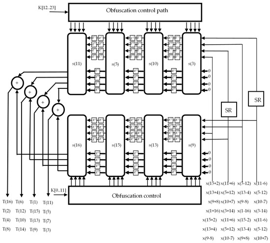
Figure 2.
The VLSI architecture for the hardware core of the 1-D DST.
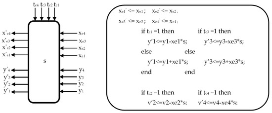
Figure 3.
The function of the processing elements from Figure 2.
Using a hardware sharing technique, four such systolic arrays have been merged into one, finally obtaining only two linear systolic arrays. We can observe that some input sequences in the two systolic arrays are identical and that the others result from a rotate and shift operation using the SR block. This fact has been exploited to significantly lower the I/O cost and to reduce the hardware complexity. It is important to mention here that the so-called I/O bottleneck that can significantly limit the speed performances has been avoided by reusing the input data in as many processing elements as possible.
Moreover, the proposed VLSI architecture can incorporate the obfuscation technique with low overheads as shown below.
In Figure 2, we have used the time-varying obfuscation technique [47,64] where the right key values are represented by and . The principle of the time-varying obfuscation technique is presented in Figure 4, where T1, …, T23 are the trigger signals, and the obfuscated signal is obtained as a combination between Ti and Ci where Ci represents the correct sign bits from Equations (61)–(64).
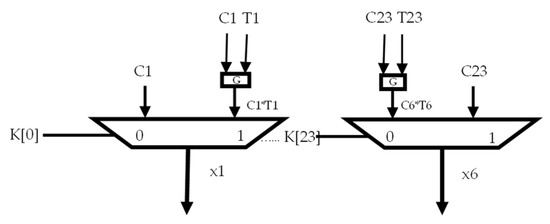
Figure 4.
Implementation of time-varying obfuscation.
The pre-processing stage implements Equations (57) and (58) and generates and arranges the input sequences. The post-processing stage computes the output sequence using Equation (60) and arranges the output sequence in the natural order.
As it can be observed from Table 3, the proposed solution has a low hardware complexity while maintaining a high throughput. It can also be seen that our solution has a double throughput as compared with [36,41] and allows for a reduced complexity of the hardware core presented in Figure 2 since it requires only adders for its hardware implementation. Moreover, the critical computation path can be further reduced by using two-level pipelining. It requires two multipliers in the post-processing stage. Additionally, our solution allows an efficient incorporation of the obfuscation technique that is not presented in the other solutions.
Table 3.
Comparison of the hardware complexity of various DST designs.
In Table 4 and Table 5, the results of the synthesis in terms of delay, power, and area of the RTL description of the DST processing chain are presented. The synthesis was performed using Cadence Genus 19.16 using the Nangate OpenCell Library with NCSU’s 15 nm FreePDK15.
Table 4.
Summary of the synthesis results (delay, power) of the DST processing chain.
Table 5.
Summary of the synthesis results (area) of the DST processing chain.
The implementation uses a fixed-point representation for the data, and the width for the and inputs and outputs of the processing elements has been set to 12 bits (although the parametric nature of the RTL descriptions allows for a simple reconfiguration of the bus data width).
The translation to the gate level description has been done several times, setting different constraints on the system clock period (from 50 ns to 150 ps).
The DST chain can operate at a potential frequency of 5.71 GHz, while dissipating a power of 36.4 mW at this frequency. When setting the target operating clock period lower than 175 ps, the synthesis tool fails to find a solution within the constraints. The lowest achievable operating clock period is 161 ps, corresponding to a frequency of 6.21 GHz, for which the area increases by about 40% compared to the results with critical path delays close to 200 ps.
To achieve a lower power dissipation, the clock frequency must be reduced. We have obtained a reduced area of about 4000 um2 and also a low power consumption that attains the value of 0.46 mW at a frequency of 100 MHz while maintaining high-speed performances. The proposed architecture can operate at a frequency of up to 6.5 GHz, generating four samples for each clock cycle. The critical path is about 200 ps, which allows a high-speed operation of the circuit.
Remarks. Using some of the ideas of the existing systolic array VLSI implementation and an appropriate reformulation of the DST algorithm based on some regular and modular computational structures, we have shown that it is possible to efficiently use the hardware structure using the systolic array architectural paradigm and, even more important, in a such way that a very efficient use of the SD representation can be obtained, leading to a maximization of the advantages of the SD representation as reduced hardware complexity and, at the same time, high-speed performance.
4. Discussion
As known, systolic arrays allow an efficient use of the hardware structures while maintaining high-speed performances using pipelining and parallelism. In our VLSI implementation, we have four systolic arrays working in parallel and, by using pipelining, we have further improved the speed performances. We also used a hardware-sharing technique to efficiently unify the four systolic arrays for the first part and of the other four for the second part of the VLSI algorithm, leading to reduced hardware complexity. Moreover, since the VLSI algorithm has been appropriately reformulated in a such manner that an efficient utilization of an optimal SD representation has been obtained, we have further significantly improved the speed performances and, at the same time, have reduced the hardware complexity. Thus, the proposed implementation can compute four samples for each clock cycle, the frequency of which can be increased up to 6.5 GHz by significantly reducing the critical path delay to about 200 ps. With the use of the presented methods, the obtained area has been significantly reduced to about 4500 um2, while the power consumption can be as low as 0.46 mW. Moreover, the proposed solution allows for an efficient incorporation of the hardware security techniques at a low overhead, which is very important for common goods devices.
5. Conclusions and Perspectives
In this paper, we have presented a unified overview of some of the most important VLSI implementations of the forward and inverse discrete sine transforms using systolic arrays. The main features of these VLSI implementation solutions using systolic arrays are presented in a unified way. Thus, one of the central ideas presented shows the advantages of using regular and modular computational structures such as cyclic convolution, circular correlation, and pseudo-band correlation in the VLSI implementation of these transforms. Additionally, due to the regular and modular nature of systolic arrays that are well suited to the features of the VLSI technologies, the efficient use of the hardware structures and low I/O costs allow avoiding of the so-called I/O bottleneck.
We have shown that by applying the ideas presented in this review, we can obtain a new VLSI implementation of the DST using systolic arrays that allow for an efficient hardware implementation with reduced hardware complexity while maintaining high-speed performances. We have used a completely new restructuring input sequence that avoids reversing the input sequence and can be used to efficiently reformulate the computation of the forward DST transform into a special computational structure based on eight short quasi-cycle convolutions with a special form and structure. The partial results can be computed in parallel and shared because some coefficients are similar, leading to a low complexity and a high throughput. As the new restructuring sequence uses the input samples in a natural order as opposed to existing solutions, a significant reduction of the hardware complexity in the pre-processing stage due to avoidance of the necessity of a permutation stage to reverse the order can be achieved. Moreover, the proposed VLSI architecture allows for an efficient incorporation of the obfuscation technique with very low overheads. For future developments, we aim to find other regular and modular computational structures for efficient VLSI implementations of the forward and inverse DST using systolic arrays.
Author Contributions
Conceptualization, D.F.C.; methodology, D.F.C. and A.C.; software, D.F.C., A.C. and V.-D.A.; validation, D.F.C. and A.C.; formal analysis, D.F.C. and A.C.; investigation, D.F.C., A.C. and V.-D.A.; writing, original draft preparation, D.F.C. and A.C.; writing, review, and editing, D.F.C. and A.C.; visualization, D.F.C. and A.C.; supervision, D.F.C.; project administration, D.F.C.; funding acquisition, D.F.C. All authors have read and agreed to the published version of the manuscript.
Funding
This work was supported by a grant from the Romanian Ministry of Education and Research, CNCS–UEFISCDI, project number PCE 172 (PN-III-P4-ID-PCE2020-0713), within PNCDI III.
Institutional Review Board Statement
Not applicable.
Informed Consent Statement
Not applicable.
Data Availability Statement
Not applicable.
Acknowledgments
The authors would like to thank the Romanian Ministry of Education and Research for their support in offering the grant CNCS–UEFISCDI, project number PCE 172 (PN-III-P4-ID-PCE2020-0713, within PNCDI III).
Conflicts of Interest
The authors declare no conflict of interest.
References
- Hilbert, P.; Lopez, M. The World’s Technological Capacity to Store, Communicate, and Compute Information. Science 2011, 332, 60–65. [Google Scholar] [CrossRef] [PubMed] [Green Version]
- Kane, G.C.; Pear, A. The Rise of Visual Content Online. MIT Sloan Management Review. Available online: https://sloanreview.mit.edu/article/the-rise-of-visual-content-online/ (accessed on 4 April 2021).
- Jain, A.K. A fast Karhunen-Loeve transform for a class of random processes. IEEE Trans. Commun. 1976, 24, 1023–1029. [Google Scholar] [CrossRef]
- Ahmed, N.; Natarajan, T.; Rao, K.R. Discrete cosine transform. IEEE Trans. Comput. 1974, 23, 90–94. [Google Scholar] [CrossRef]
- Jain, A.K. Fundamentals of Digital Image Processing; Prentice Hall: Englewood Cliffs, NJ, USA, 1989. [Google Scholar]
- Kalali, E.; Mert, A.C.; Hamzaoglu, I. A computation and energy reduction technique for HEVC Discrete Cosine Transform. IEEE Trans. Consum. Electron. 2016, 62, 166–174. [Google Scholar] [CrossRef]
- Ali, M.; Islam, M.; Memon, M.; Asif, D.M.; Lin, F. Optimum DCT type-I based transceiver model and effective channel estimation for uplink NB-IoT system. Phys. Commun. 2021, 48, 101431. [Google Scholar] [CrossRef]
- Domínguez-Jiménez, M.E.; Luengo, D.; Sansigre-Vidal, G.; Cruz-Roldán, F. A novel channel estimation scheme for multicarrier communications with the Type-I even discrete cosine transform. In Proceedings of the 2017 25th European Signal Processing Conference (EUSIPCO), Kos, Greece, 28 August–2 September 2017; pp. 2239–2243. [Google Scholar]
- Domínguez-Jiménez, M.E.; Luengo, D.; Sansigre-Vidal, G.; Cruz-Roldán, F. A Novel Scheme of Multicarrier Modulation with the Discrete Cosine Transform. IEEE Trans. Wirel. Commun. 2021, 20, 7992–8005. [Google Scholar] [CrossRef]
- Lee, C.F.; Shen, J.J.; Chen, Z.R.; Agrawal, S. Self-Embedding Authentication Watermarking with Effective Tampered Location Detection and High-Quality Image Recovery. Sensors 2019, 19, 2267. [Google Scholar] [CrossRef] [Green Version]
- Lu, W.; Chen, Z.; Li, L.; Cao, X.; Wei, J.; Xiong, N.; Li, J.; Dang, J. Watermarking Based on Compressive Sensing for Digital Speech Detection and Recovery. Sensors 2018, 18, 2390. [Google Scholar] [CrossRef] [Green Version]
- Boukhechba, K.; Wu, H.; Bazine, R. DCT-Based Preprocessing Approach for ICA in Hyperspectral Data Analysis. Sensors 2018, 18, 1138. [Google Scholar] [CrossRef] [Green Version]
- Xu, P.; Chen, B.; Xue, L.; Zhang, J.; Zhu, L. A Prediction-Based Spatial-Spectral Adaptive Hyperspectral Compressive Sensing Algorithm. Sensors 2018, 18, 3289. [Google Scholar] [CrossRef] [Green Version]
- Kamisli, F. Lossless Image and Intra-Frame Compression with Integer-to-Integer DST. IEEE Trans. Circuits Syst. Video Technol. 2019, 29, 502–516. [Google Scholar] [CrossRef] [Green Version]
- Panda, J.; Meher, S. A Novel Approach of Image Interpolation using DST. In Proceedings of the 2019 Fifth International Conference on Image Information Processing (ICIIP), Shimla, India, 15–17 November 2019. [Google Scholar]
- Ajmera, A.; Divecha, M.; Ghosh, S.S.; Raval, I.; Chaturvedi, R. Video Steganography: Using Scrambling-AES Encryption and DCT, DST Steganography. In Proceedings of the 2019 IEEE Pune Section International Conference (PuneCon), Pune, India, 18–20 December 2019. [Google Scholar]
- Lu, K.-S.; Ortega, A.; Mukherjee, D.; Chen, Y. DCT and DST Filtering with Sparse Graph Operators. IEEE Trans. Signal Process. 2022, 70, 1641–1656. [Google Scholar] [CrossRef]
- Rose, K.; Heiman, A.; Dinstein, I. DCT/DST alternate-transform of image coding. IEEE Trans. Commun. 1990, 38, 94–101. [Google Scholar] [CrossRef]
- Koc, U.T.; Ray Liu, K.J. Discrete Cosine/sine transform based motion estimation. In Proceedings of the 1994 1st International Conference on Image Processing, Austin, TX, USA, 13–16 November 1994; pp. 771–775. [Google Scholar]
- Cinemre, I.; Hacioglu, G. A DCT/DST Based Fast OFDM Method in IM/DD Systems. IEEE Commun. Lett. 2021, 25, 3013–3016. [Google Scholar] [CrossRef]
- Guo, J.I.; Liu, C.M.; Jen, C.W. A New Array Architecture for Prime-Length Discrete Cosine Transform. IEEE Trans. Signal Process. 1993, 41, 436. [Google Scholar]
- Chiper, D.F. A new systolic array algorithm for memory-based VLSI array implementation of DCT. In Proceedings of the 1997 Proceedings Second IEEE Symposium on Computers and Communications, Alexandria, Egypt, 1–3 July 1997; pp. 297–301. [Google Scholar]
- Meher, P.K. Systolic designs for DCT using low-complexity concurrent convolutional formulation. IEEE Trans. Circuits Syst. Video Technol. 2006, 16, 1041–1050. [Google Scholar] [CrossRef]
- Chiper, D.F.; Ungureanu, P. Novel VLSI Algorithm and Architecture with Good Quantization Properties for a High-Throughput Area Efficient Systolic Array Implementation of DCT. EURASIP J. Adv. Signal Process. 2010, 2011, 639043. [Google Scholar] [CrossRef]
- Chan, Y.H.; Siu, W.C. Generalized approach for the realization of discrete cosine transform using cyclic convolutions. In Proceedings of the 1993 IEEE Conference on Acoustic, Speech, and Signal Processing, Minneapolis, MN, USA, 27–30 April 1993; pp. 277–280. [Google Scholar]
- Chan, Y.H.; Siu, W.C. On the realization of discrete cosine transform using the distributed arithmetic. IEEE Trans. Circuits Syst. I: Regul. Pap. 1992, 39, 705–712. [Google Scholar] [CrossRef]
- Nikara, J.; Takola, J.; Akopian, D.; Saarinen, J. Pipeline architecture for DCT/IDCT. In Proceedings of the ISCAS 2001, the 2001 IEEE International Symposium on Circuits and Systems, Sydney, Australia, 6–9 May 2001; pp. 902–905. [Google Scholar]
- Chiper, D.F.; Swamy, M.N.S.; Ahmad, M.O. An efficient unified framework for the VLSI implementation of a prime-length DCT/IDCT with high throughput. IEEE Trans. Signal Process. 2007, 55, 2925–2936. [Google Scholar] [CrossRef]
- Cheng, C.; Parhi, K.K. A novel systolic array structure for DCT. IEEE Trans. Circuits Syst. II Express Briefs 2005, 52, 366–369. [Google Scholar] [CrossRef]
- Chiper, D.F. A New VLSI algorithm and Architecture for the hardware implementation of type IV discrete cosine transform using a pseudo-band correlation structure. Cent. Eur. J. Comput. Sci. 2011, 1, 90–97. [Google Scholar] [CrossRef]
- Chiper, D.F. New VLSI Algorithm for a High-Throughput Implementation of Type IV DCT. In Proceedings of the 2016 International Conference on Communications (COMM), Bucharest, Romania, 9–10 June 2016. [Google Scholar]
- Cheng, C.; Parhi, K.K. Hardware efficient fast DCT based on novel cyclic convolution structures. IEEE Trans. Signal Process. 2006, 54, 4419–4434. [Google Scholar] [CrossRef]
- Xie, J.; Meher, P.K.; He, J. Hardware-Efficient Realization of Prime-Length DCT Based on Distributed Arithmetic. IEEE Trans. Comput. 2013, 62, 1170–1178. [Google Scholar] [CrossRef]
- Chiper, D.F. A parallel VLSI algorithm for a high throughput systolic array VLSI implementation of type IV DCT. In Proceedings of the 2009 International Symposium on Signals, Circuits and Systems (ISSCS2009), Iasi, Romania, 9–10 July 2009; pp. 257–260. [Google Scholar]
- Pan, S.B.; Park, R.-H. Unified systolic array for computation of DCT/DST/DHT. IEEE Trans. Circuits Syst. Video Technol. 1997, 7, 413–419. [Google Scholar]
- Chiper, D.F.; Swamy, M.N.S.; Ahmad, M.O.; Stouraitis, T. Systolic Algorithm Algorithms and Algorithm a Memory-Based Design Approach for a Unified Architecture for the Computation of DCT/DST/IDCT/IDST. IEEE Trans. Circuits Syst.-I Regul. Pap. 2005, 52, 1125–1137. [Google Scholar] [CrossRef]
- Meher, P.K.; Swamy, M.N.S. New Systolic Algorithm and Array Architecture for Prime-Length Discrete Sine Transform. IEEE Trans. Circuits Syst. II Express Briefs 2007, 54, 262–266. [Google Scholar] [CrossRef]
- Chiper, D.F.; Cracan, A.; Burdia, D. A new systolic array algorithm and architecture for the VLSI implementation of IDST based on a pseudo-band correlation structure. Adv. Electr. Comput. Eng. 2017, 17, 75–80. [Google Scholar] [CrossRef]
- Chiper, D.F.; Cracan, A. An Efficient Algorithm for the VLSI Implementation of the Inverse DST Based on Quasi-Band Correlation Structures. In Proceedings of the 2021 International IEEE Symposium on Circuits and Systems (ISSCS2021), Iasi, Romania, 15–16 July 2021. [Google Scholar]
- Chiper, D.F.; Cracan, A. A novel algorithm and architecture for a high-throughput VLSI implementation of DST using short pseudo-cycle convolutions. In Proceedings of the 2017 International Symposium on Signals, Circuits and Systems (ISSCS), Iasi, Romania, 13–14 July 2017. [Google Scholar]
- Chiper, D.F.; Swamy, M.N.S.; Ahmad, M.O.; Stouraits, T. A systolic array architecture for the discrete sine transform. IEEE Trans. Signal Process. 2002, 50, 2347–2354. [Google Scholar] [CrossRef]
- Chakraborty, R.S.; Bhunia, S. Security against hardware Trojan through a novel application of design obfuscation. In Proceedings of the 2009 IEEE/ACM International Conference on Computer-Aided Design-Digest of Technical Papers, San Jose, CA, USA, 2–5 November 2009; pp. 113–116. [Google Scholar]
- Pilato, C.; Garg, S.; Wu, K.; Karri, R.; Regazzoni, F. Securing hardware accelerators: A new challenge for high-level synthesis. IEEE Embed. Syst. Lett. 2018, 10, 77–80. [Google Scholar] [CrossRef]
- Shamsi, K.; Li, M.; Meade, T.; Zhao, Z.; Pan, D.Z.; Jin, Y. AppSAT: Approximately deobfuscating integrated circuits. In Proceedings of the 2017 IEEE International Symposium on Hardware Oriented Security and Trust (HOST), Mclean, VA, USA, 1–5 May 2017; pp. 95–100. [Google Scholar]
- Sengupta, A.; Roy, D.; Mohanty, S.P.; Corcoran, P. Low-cost obfuscated JPEG CODEC IP core for secure CE hardware. IEEE Trans. Consum. Electron. 2018, 64, 365–374. [Google Scholar] [CrossRef]
- Zhang, J. A practical logic obfuscation technique for hardware security. IEEE Trans. Very Large Scale Integr. (VLSI) Syst. 2016, 24, 1193–1197. [Google Scholar] [CrossRef]
- Koteshwara, S.; Kim, C.H.; Parhi, K.K. Key-Based Dynamic Functional Obfuscation of Integrated Circuits Using Sequentially Triggered Mode-Based Design. IEEE Trans. Inf. Forensics Secur. 2018, 13, 79–93. [Google Scholar] [CrossRef]
- Parhi, K.K.; Koteshwara, S. Dynamic Functional Obfuscation. U.S. Patent 15/667 776, 3 August 2017. [Google Scholar]
- Koteshwara, S.; Kim, C.H.; Parhi, K.K. Hierarchical functional obfuscation of integrated circuits using a mode-based approach. In Proceedings of the 2017 IEEE International Symposium on Circuits and Systems (ISCAS), Baltimore, MD, USA, 28–31 May 2017. [Google Scholar]
- Kung, S.Y. VLSI Array Processors; Prentice Hall: Englewood Cliffs, NJ, USA, 1988. [Google Scholar]
- Jen, C.W.; Hsu, H.Y. The design of systolic arrays with tag input. In Proceeding of the International Symposium on Circuits and Systems, Espoo, Finland, 7–9 June 1988; pp. 2263–2266. [Google Scholar]
- Parvin, A.; Ahmadi, M.; Muscedere, R. Application of neural networks with CSD coefficients for human face recognition. In Proceedings of the 2013 IEEE International Symposium on Circuits and Systems (ISCAS), Beijing, China, 19–23 May 2013; pp. 1628–1631. [Google Scholar]
- Pinjare, S.L.; Kumar, E.H. Implementation of Artificial Neural Network Architecture for Image Compression Using CSD Multiplier. In Proceedings of the 2013 International Conference on Emerging Research in Computing, Information, Communication and Applications (ERCICA), Baku, Azerbaijan, 23–25 October 2013; pp. 581–587. [Google Scholar]
- Ahn, B.; Kim, T. Deeper Weight Pruning Without Accuracy Loss in Deep Neural Networks: Signed-Digit Representation-Based Approach. IEEE Trans. Comput.-Aided Des. Integr. Circuits Syst. 2022, 41, 656–668. [Google Scholar] [CrossRef]
- Riaz, M.; Hafiz, R.; Khaliq, S.A.; Faisal, M.; Iqbal, H.T.; Ali, M.; Shafique, M. CAxCNN: Towards the Use of Canonic Sign Digit Based Approximation for Hardware-Friendly Convolutional Neural Networks. IEEE Access 2020, 8, 127014–127021. [Google Scholar] [CrossRef]
- Cardarilli, G.C.; Di Nunzio, L.; Fazzolari, R.; Nannarelli, A.; Re, M. Approximated Canonical Signed Digit for Error Resilient Intelligent Computation. In Proceedings of the 2019 53rd Asilomar Conference on Signals, Systems, and Computers, Pacific Grove, CA, USA, 3–6 November 2019. [Google Scholar]
- Mahdavi, H.; Timarchi, S. Area–Time–Power Efficient FFT Architectures Based on Binary-Signed-Digit CORDIC. IEEE Trans. Circuits Syst. I Regul. Pap. 2019, 66, 3874–3881. [Google Scholar] [CrossRef]
- Peled, A. On the Hardware Implementation of Digital Signal Processors. IEEE Trans. Acoust. Signal Proc. 1976, 24, 76–86. [Google Scholar] [CrossRef]
- Hashmian, R. A new method for conversion of a 2’s complement to canonic signed digit number system and its representation. In Proceedings of the Conference Record of The Thirtieth Asilomar Conference on Signals, Systems and Computers, Pacific Grove, CA, USA, 3–6 November 1996. [Google Scholar]
- Rezai, A.; Keshavarzi, P. Compact SD: A new encoding algorithm and its application in multiplication. Int. J. Comput. Math. 2017, 94, 554–569. [Google Scholar] [CrossRef]
- Rezai, A.; Keshavarzi, P. CCS Representation: A New Non-Adjacent Form and its Application in ECC. J. Basic. Appl. Sci. Res. 2012, 2, 4577–4586. [Google Scholar]
- Joye, M.; Yen, S.M. Optimal left-to-right binary signed-digit recoding. IEEE Trans. Comput. 2000, 49, 740–748. [Google Scholar] [CrossRef] [Green Version]
- Zaman, K.S.; Reaz, M.B.I.; Bakar, A.A.A.; Bhuiyan, M.A.S.; Mohd, N.A.; Mokhtar, H.H.B.; Ali, S.H. Minimum signed digit approximation for faster and more efficient convolutional neural network computation on embedded devices. Eng. Sci. Technol. Int. J. 2022, 36, 101153. [Google Scholar] [CrossRef]
- Chiper, D.F.; Cotorobai, L. A New VLSI Algorithm for type IV DCT for an Efficient Implementation of Obfuscation Technique. In Proceedings of the 2020 43rd International Conference on Telecommunications and Signal Processing (TSP), Milan, Italy, 7–9 July 2020. [Google Scholar]
Publisher’s Note: MDPI stays neutral with regard to jurisdictional claims in published maps and institutional affiliations. |
© 2022 by the authors. Licensee MDPI, Basel, Switzerland. This article is an open access article distributed under the terms and conditions of the Creative Commons Attribution (CC BY) license (https://creativecommons.org/licenses/by/4.0/).