Article

High-Level Design Optimizations for Implementing Data Stream Sketch Frequency Estimators on FPGAs

Department of Computer Engineering, University of Bahrain, Sakhir P.O. Box 32038, Bahrain
Electronics 2022, 11(15), 2399; https://doi.org/10.3390/electronics11152399
Submission received: 4 July 2022 / Revised: 25 July 2022 / Accepted: 28 July 2022 / Published: 31 July 2022
(This article belongs to the Special Issue Recent FPGA Architectures and Applications)

Abstract

:
This paper presents simple yet effective optimizations for implementing data stream frequency estimation sketch kernels using High-Level Synthesis (HLS). The paper addresses design issues common to sketches utilizing large portions of the embedded RAM resources in a Field Programmable Gate Array (FPGA). First, a solution based on Load-Store Queue (LSQ) architecture is proposed for resolving the memory dependencies associated with the hash tables in a frequency estimation sketch. Second, performance fine-tuning through high-level pragmas is explored to achieve the best possible throughput. Finally, a technique based on pre-processing the data stream in a small cache memory prior to updating the sketch is evaluated to reduce the dynamic power consumption. Using an Intel HLS compiler, a proposed optimized hardware version of the popular Count-Min sketch utilizing 80% of the embedded RAM in an Intel Arria 10 FPGA, achieved more than 3x the throughput of an unoptimized baseline implementation. Furthermore, the sketch update rate is significantly reduced when the input stream is skewed. This, in turn, minimizes the effect of high throughput on dynamic power consumption. Compared to FPGA sketches in the published literature, the presented sketch is the most well-rounded sketch in terms of features and versatility. In terms of throughput, the presented sketch is on a par with the fastest sketches fine-tuned at the Register Transfer Level (RTL).

1. Introduction

Data stream algorithms aim to extract useful insight from large streams of data modeled as a sequence of items that can only be processed once using limited memory. In general, processing speed is a major focus in streaming algorithms because of the high-speed nature of the data and the lack of random access to the input. Streaming algorithms are typically single-pass approximate algorithms as exact solutions are not feasible, due to the time and memory complexity in data stream applications [1]. A distinct class of streaming algorithms addresses the frequency estimation problem, wherein a small summary of the input frequency distribution is constructed from the data stream. This summary can be queried to estimate the frequency of the unique items in the stream. Estimating how often items are appearing in the data is a fundamental task in many applications. Frequency estimation has several applications in networking [2], web search analysis and databases [3], signal processing and machine learning [4], among many other fields. Items of interest in a data stream could represent popular search queries in a server, frequently visited websites in network traffic, best-selling items in retail data, most active stocks in financial data, etc.
Sketching is an emerging technique that deploys a unique data structure referred to as a “sketch” or a “sketch summary” to solve several streaming problems, including frequency estimation. Notable frequency estimation sketches include AMS [5], Count [6], and Count-Min [7]. These sketches are fundamentally similar, consisting of several “item counting” hash tables with a size in memory adjusted according to the required accuracy. In addition to being very memory efficient, parallelizing the operation of these sketch summaries is quite straightforward, as updating the different hash tables can be performed in separate parallel tasks.
Several hardware architectures have been proposed to capitalize on the parallelism possible with frequency estimation sketches. Mainly, these architectures are implemented using Field Programmable Gate Arrays (FPGAs), due to the two following reasons: (1) the flexibility in implementing sketches tailored to specific streams and applications, and (2) the high-bandwidth low-latency embedded memory available in FPGAs. Although high-density FPGAs offer sufficient on-chip memory to implement practical sketches, maintaining high throughputs in sketch designs utilizing large portions of the FPGA on-chip memory can be difficult without expertise in FPGA chip planning. This issue is apparent in reconfigurable accelerators proposed in academia, that either opt for smaller sketches implemented on high-end expansive FPGA fabric or deploy simple pipelining techniques that do not scale well in large sketches.
High-Level Synthesis (HLS) tools from major FPGA vendors (Xilinx/AMD, Intel and recently Microchip) have become mature enough to be widely adopted by the industry to generate production-quality systems or components in larger systems. With the proper high-level optimizations, high-speed complex circuits can be developed and verified at a fraction of the development time typically needed in Register Transfer Level (RTL) design flow.
This paper details the optimization process of a hardware variant of the Count-Min sketch data structure. The presented optimizations only require the addition of small “weight accumulation” circuits that are simple to implement and can be generalized to other sketch summaries. In the experimental results, an optimized Count-Min sketch utilizing 80% of the on-chip RAM in a midrange Intel Arria 10 FPGA achieved more than 3x the throughput of a naïve baseline implementation. On an Intel Stratix 10 FPGA, an optimized sketch achieved throughputs significantly higher than competing FPGA sketches designed in RTL and on a par with the fastest software-generated fine-tuned sketches. In addition, the optimized sketch exhibited reduced memory access rate when processing streams with skewed frequency distribution (often the case in real-world data streams). This was shown to have great potential for reducing the dynamic power consumption of the sketch. In short, the main contributions of this paper can be summarized as follows:
(1)
A simple item weight accumulation circuit that is entirely specified at the C language level to remove dependencies associated with memory updates in frequency estimation sketches.
(2)
A scheme for scaling the performance of an HLS-generated sketch through fine-tuning the dependance distance in the memory blocks of a sketch.
(3)
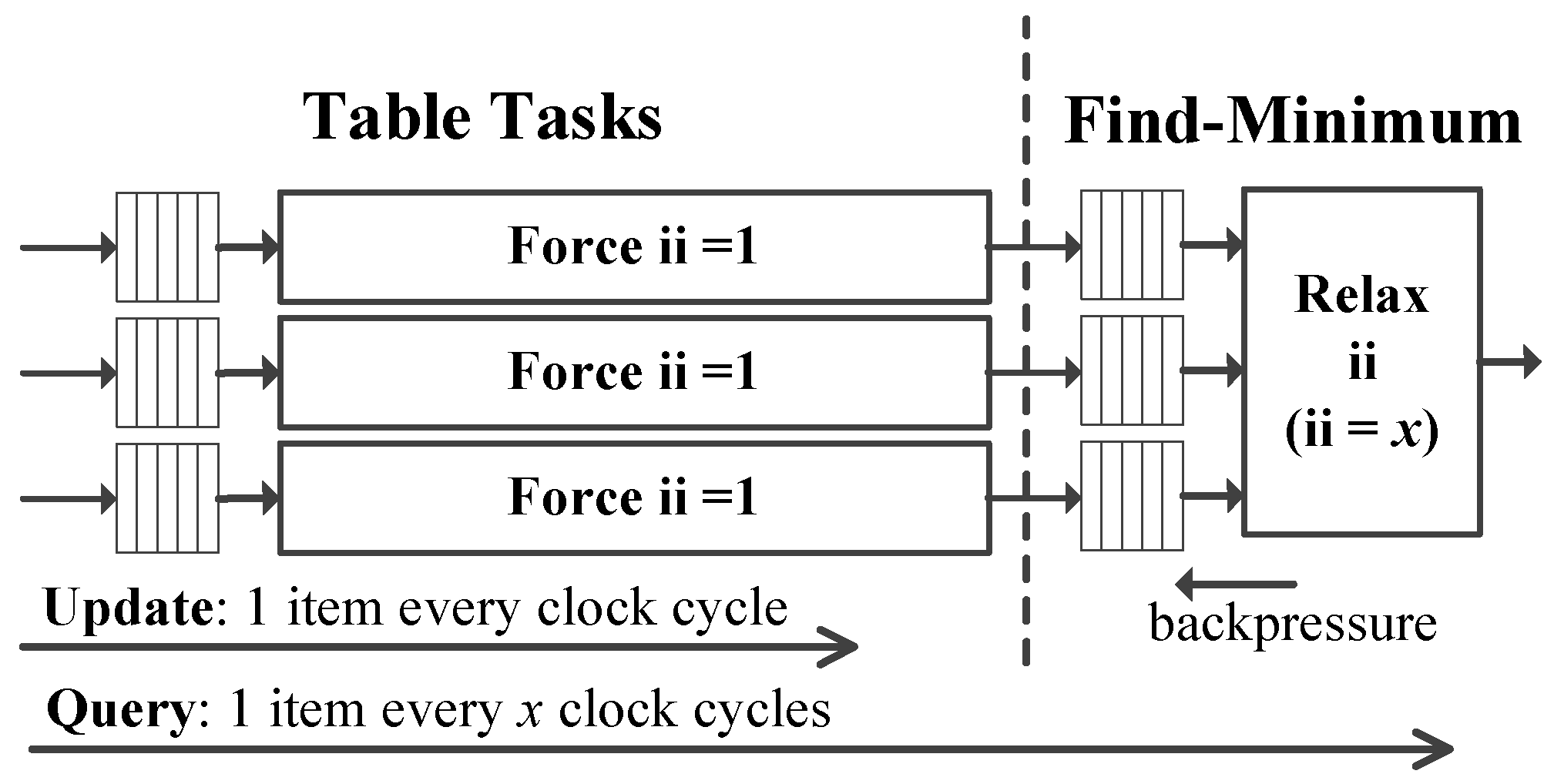
A scheme for scaling performance through partitioning the sketch into separate update/query hardware tasks that can be constrained separately.
(4)
A power-optimized sketch design that takes advantage of the natural skew in typical data streams to reduce memory accesses, and consequently reduce the overall dynamic power consumption.
(5)
The fastest and most well-rounded FPGA implementation of the popular Count-Min sketch compared to previous work.
The remainder of this paper is organized as follows. Section 2 introduces the Count-Min sketch data structure. Section 3 discusses some of the most relevant related work on FPGA frequency estimation accelerators. Section 4 presents a baseline HLS implementation of Count-Min. Section 5 and Section 6 detail the optimization process of the baseline. Section 7 presents the evaluation of the optimized sketch against previously published work. Finally, conclusions and future work plans are summarized in Section 8.
We draw the readers’ attention to the Intel HLS documentation [8], as the remainder of this paper explains the proposed optimizations using technical terminology that may be specific to Intel “System of Tasks” HLS design flow.

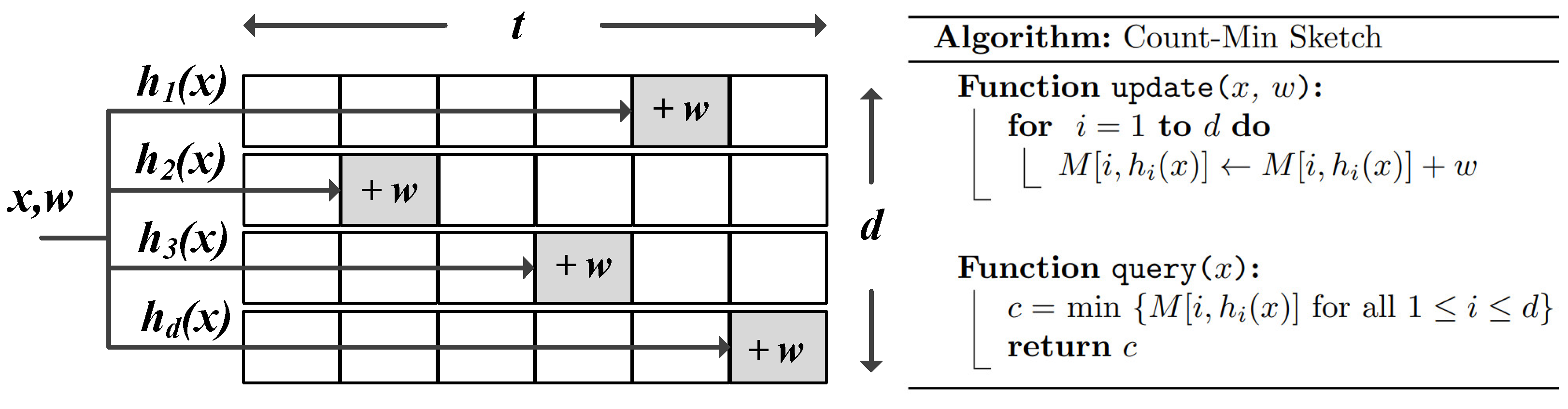
2. Background: Count-Min Sketch

The work presented in this paper is applicable to several frequency estimation sketches, such as AMS [5], Count [6], and Count-Min [7]. The Count-Min sketch was selected for implementation and evaluation as it is one of the most popular frequency estimation sketches, with applications spanning many domains. In fact, this sketch is widely adopted in the industry. For example, twitter used this sketch to track popular tweets [9], and Apple also used this sketch in their private data collection [10]. In addition, Count-Min has great support in many databases and big data analytics tools (examples: Apache Spark [11], Redis [12]).
The main goal of the algorithm behind Count-Min is to count the number of occurrences of distinct items in a stream. The sketch consists of d hash tables, each with t entries representing count estimates of items in the stream. The tables can be stored in memory as a two-dimensional array (see Figure 1). A family of pairwise independent hash functions is used to map item hits to the table entries. Count-Min supports weighted updates, meaning that any item hit, x, in the stream could have a weight value, w, associated with it.
The update process of the sketch summary is simple, in that the item key is hashed using the hash functions and the relevant count entries in the tables are incremented by the item weight. Since different hash functions are used for the different tables, item collisions will differ. This means that frequent items, which are usually the items of interest, are likely to only collide with insignificant low-frequency items in some of the tables giving accurate count estimates for the frequent items. The total count of an item in the stream can be estimated when the item is queried by taking the minimum count from the relevant table entries. The minimum count represents the entry with the least number of collisions, and, hence, the smallest count error. For the case of updates with positive weights, if W is the sum of all weights in the stream, then the count overestimation error for any item is guaranteed to be at most ɛW with probability (1 − δ). The size of the sketch is set to meet the desired accuracy by selecting t = 2/ɛ, and d = log2 1/δ. In order for Count-Min error guarantee to hold, the sketch must use pairwise independent hash functions. A common pairwise independent hash function that is used by the authors of the sketch is shown in (1). This hash function requires a large prime number p and two salts a and b that are randomly selected for each hash table.
h ( x ) = ( a x + b   m o d   p )   m o d   t

3. Related Work: FPGA-Based Data Stream Frequency Estimators

FPGAs and other hardware accelerators, such as Graphical Processing Units (GPUs), have been extensively studied for accelerating frequent itemset mining of large datasets [13], which is a task related to item frequency estimation. These itemset mining accelerators were designed to find common sets or sequences among a huge number of separate transactions, rather than counting items in a data stream. In streaming applications, in which the data is only looked at once, FPGAs tend to be more appealing than GPUs in situations that require fast processing of data where it is generated or collected (examples: network switches and sink nodes in wireless sensor networks).
FPGA data stream frequency estimation accelerators take advantage of the parallelism and deep pipelining possible in FPGAs to achieve significantly higher throughputs compared to commodity processors. Several proposed accelerators are based on systolic array architectures consisting of pipelined item-counting Processing Elements (PEs) [14,15,16,17]. These PEs store (item, count) pairs and achieve high processing rates by performing simultaneous compare-increment operations. The main disadvantage of such accelerators is that items and item counts are stored in registers implemented using the FPGA logic resources to achieve deep pipelining, and this limits the number of items that can be monitored (hundreds to a few thousands).
To enhance scalability, other approaches utilize the abundant embedded RAM resources in FPGAs to store the (item, count) pairs in hash tables. This allows for monitoring a much larger number of items and allows for representing of items with larger integers. However, the throughput can be significantly reduced due to the hash collision issue. An example is the accelerator in [18], which implements a pipelined cuckoo hash table to reduce the effect of hash collisions on throughput. A similar approach is presented in [19], where several parallel hash tables are utilized at the same time to scale performance. In general, in systems relying on generic hash tables the throughput always depends on the input distribution and will be affected by the complex dependencies associated with the hash table insertion operations.
As described in Section 2, hash collision resolution is not required in a frequency estimation sketch. In addition, table entries in a sketch do not contain the item keys and the operation of updating a table only requires incrementing the relevant table entry. Due to their simplicity and low memory footprint, FPGA accelerators, based on frequency estimation sketches, are gaining popularity. The authors in [20] detailed the RTL design process of a Count-Min sketch accelerator used for heavy hitter detection (finding items that occur frequently in a stream) and anomaly detection in network traffic data. The main obstacle in scaling the sketch was implementing hash tables with large RAM blocks while maintaining high operating frequency. This was addressed by manually partitioning the large RAM blocks into smaller pipelined blocks. Manual RAM pipelining scaled well for medium-sized sketches; however, large sketches suffered a significant drop in throughput. A similar RAM pipelining technique is used in the software sketch generator tool presented in [21]. This tool can be used to generate a sketch with user specified parameters, such as the sketch size and desired throughput. It works alongside the FPGA vendor tools (Xilinx and Intel) to come up with a configuration that meets the user specified parameters. The process iterates over several compilations until the sketch is fine-tuned to the desired parameters. The tool can generate sketches with very high throughputs that can be considered optimal for the supported FPGA families. However, according to the authors, the fine-tuning process can take up to two weeks for larger sketches implemented on large FPGA chips.
Other sketch design strategies avoid using large sketches to sustain high throughputs. Using smaller sketches comes at the expense of reduced accuracy. This can be justified in some applications. For example, the authors in [22,23] used a small sketch based on a well-known optimized variant of Count-Min, alongside a priority queue data structure to maintain an approximate list of the top items in the stream. This list was used to estimate the entropy of the stream in a process that can tolerate the reduced accuracy imposed by the smaller sketch size. A similar hardware sketch based on the same Count-Min algorithm extension was presented in [24] for heavy hitter detection in data streams.
While the sketches in [22,23,24] are based on a well-known size-optimized variant of Count-Min with proven error bounds, other implementations modify the sketch algorithm to make it more efficient for hardware implementation without formal error analysis. The implementations in [25,26] heavily modified the Count-Min sketch to gain more accuracy out of a smaller high-throughput sketch. The algorithm modifications cannot be generalized for all use cases of Count-Min and break its error guarantee, which is very important in most applications.
An interesting property of some sketches is the ability to merge separate sketches with identical parameters by summing them up, entry-wise. This can be very useful in large distributed systems. The authors in [21,27] demonstrated how implementing several replicas of a Count-Min sketch on the same FPGA chip can significantly boost throughput by processing several parallel streams at the same time. Considering that the on-chip memory is relatively limited, implementing multiple replicas of a smaller sketch on a single chip entails a significant accuracy compromise. For example, having two replicas of the same sketch would double the memory requirement for the same accuracy. In many applications, a more practical approach to implement Count-Min on an FPGA is to scale the size of a single sketch as much as possible to extract the best accuracy from the FPGA chip while trying to maintain a high throughput.
In a typical FPGA implementation of Count-Min, embedded RAM is the dominant resource type. As RAM access is known to be a major contributor to dynamic power consumption in FPGAs, especially at high clock rates, the increase in dynamic power in large high-throughput sketches might be significant. To our knowledge, the sketch in [28] is the only hardware sketch to be optimized for low power consumption. This sketch is aimed at small energy-harvesting devices and works simply by deploying a filtering stage that blocks portions of the stream to reduce RAM accesses at the expense of reduced accuracy.

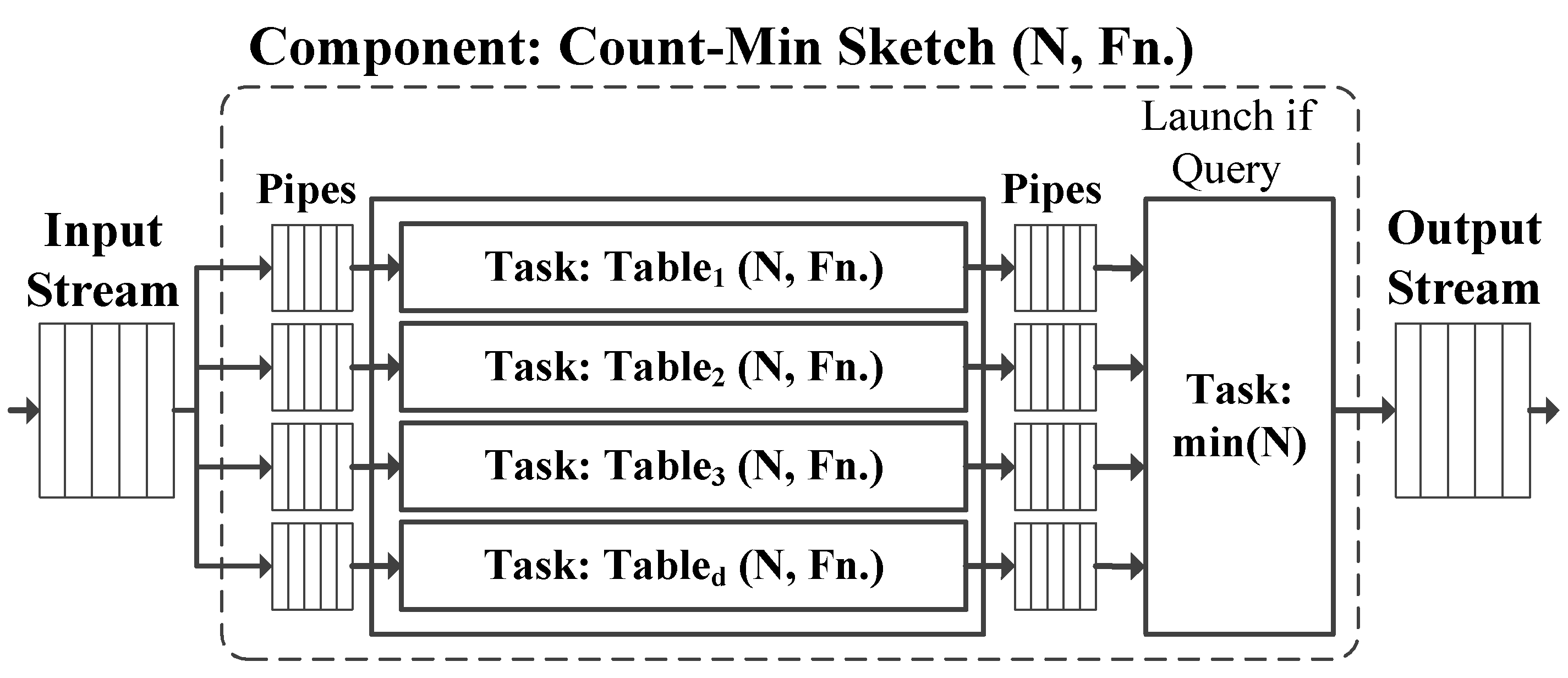
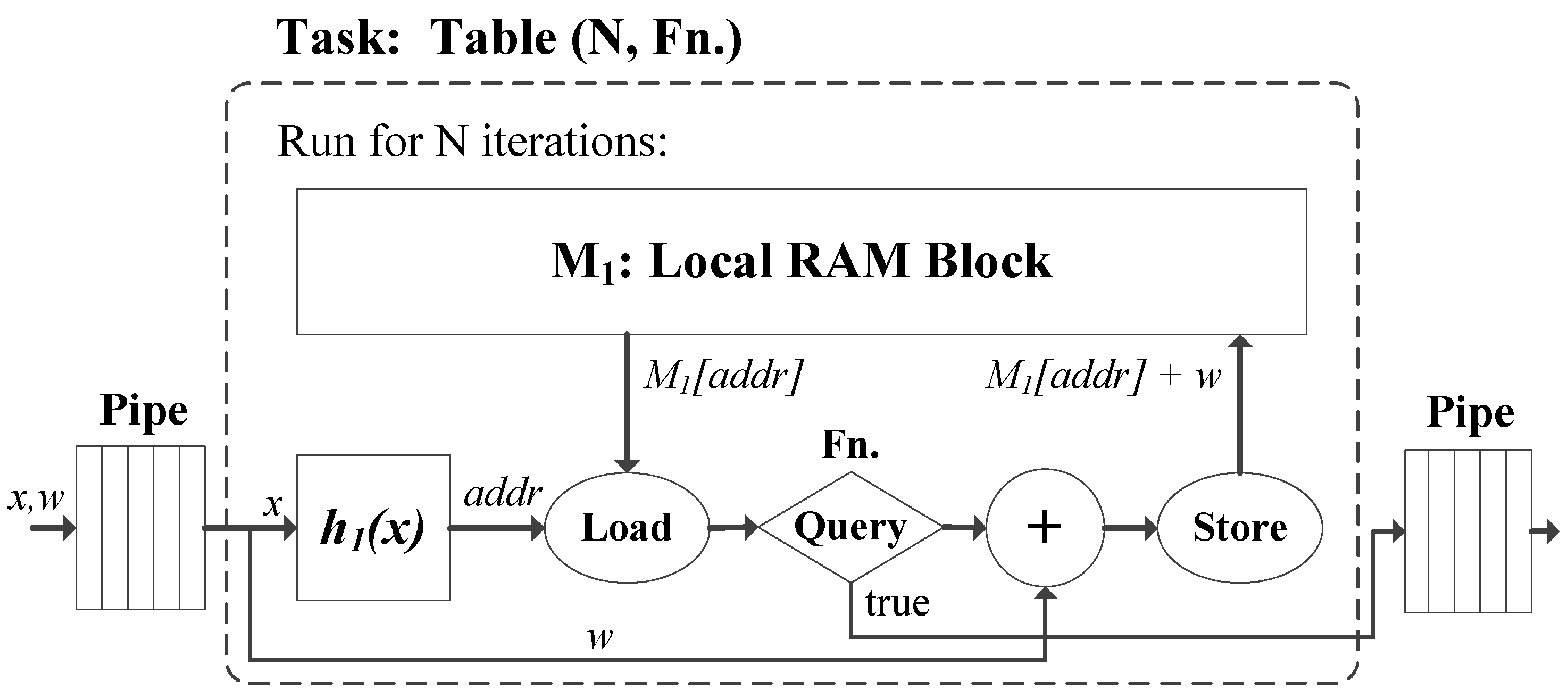
4. Baseline FPGA Implementation

Intel “System of Tasks” HLS design flow allows for parallel hardware tasks to be launched asynchronously from a top-level component [8]. An efficient Count-Min sketch can be easily realized using this design flow. Figure 2 shows the basic building blocks of a Count-Min sketch component with standard input and output streaming interfaces. The component can be invoked with two stable arguments (N and Fn.). N is the number of items consumed by the component in a single invocation, and Fn. is the main function executed by the sketch (update or query). When invoked in update mode, the component launches d hash table tasks and writes copies of the input stream data to separate internal pipes that feed these tasks. A block diagram of a hash table task is shown in Figure 3. In a hash table task, every item from the input pipe is hashed using the hash function in (1) and the relevant location in a static RAM block with t memory locations is incremented by the item weight. This operation is executed for N iterations before the task returns. It is noted that the hash function random salts and the prime numbers needed in the different hash table tasks are generated offline and stored as constants.
In query mode, the N items that need to be queried are written to the input stream with zero weights when the sketch component is invoked. The sketch component launches the hash table tasks as well as a “find-minimum” task. In this mode, the hash table tasks read the relevant count estimates from the RAM blocks and write to internal pipes. The find-minimum task reads these internal pipes and writes the minimum values to the output stream.
Although the RAM resources in modern FPGAs can be configured to implement blocks with dual-port capability, allowing for simultaneous load and store operations, compiling the hash table task shown in Figure 3 would result in a circuit with an initiation interval (ii) larger than 1 (ii is the number of clock cycles between the launch of successive loop iterations). This occurs because the compiler inserts stalling logic to protect against data hazards related to memory dependency. Without stalling the task pipeline, consecutive updates to the same RAM address cause functional failure because of memory latency and the read-after-write data hazard. As on-chip RAM blocks in FPGAs have a typical latency of 1 clock cycle, the best achievable ii would be 2.
A straightforward approach to mitigate the effect of higher ii on the throughput without modifying the sketch pipeline is to de-multiplex the stream among several parallel replicas of the sketch. This way, one or more items can be consumed every clock cycle by the sketch combination. This technique has been demonstrated in the FPGA accelerator in [29], which implemented the HyperLogLog sketch to measure the cardinality of a stream. This technique, however, significantly limits the possible accuracy when implementing a frequency estimation sketch on an FPGA, as the memory requirements are much higher for frequency estimation sketches compared to cardinality estimation sketches.

5. Optimizing for High Throughput

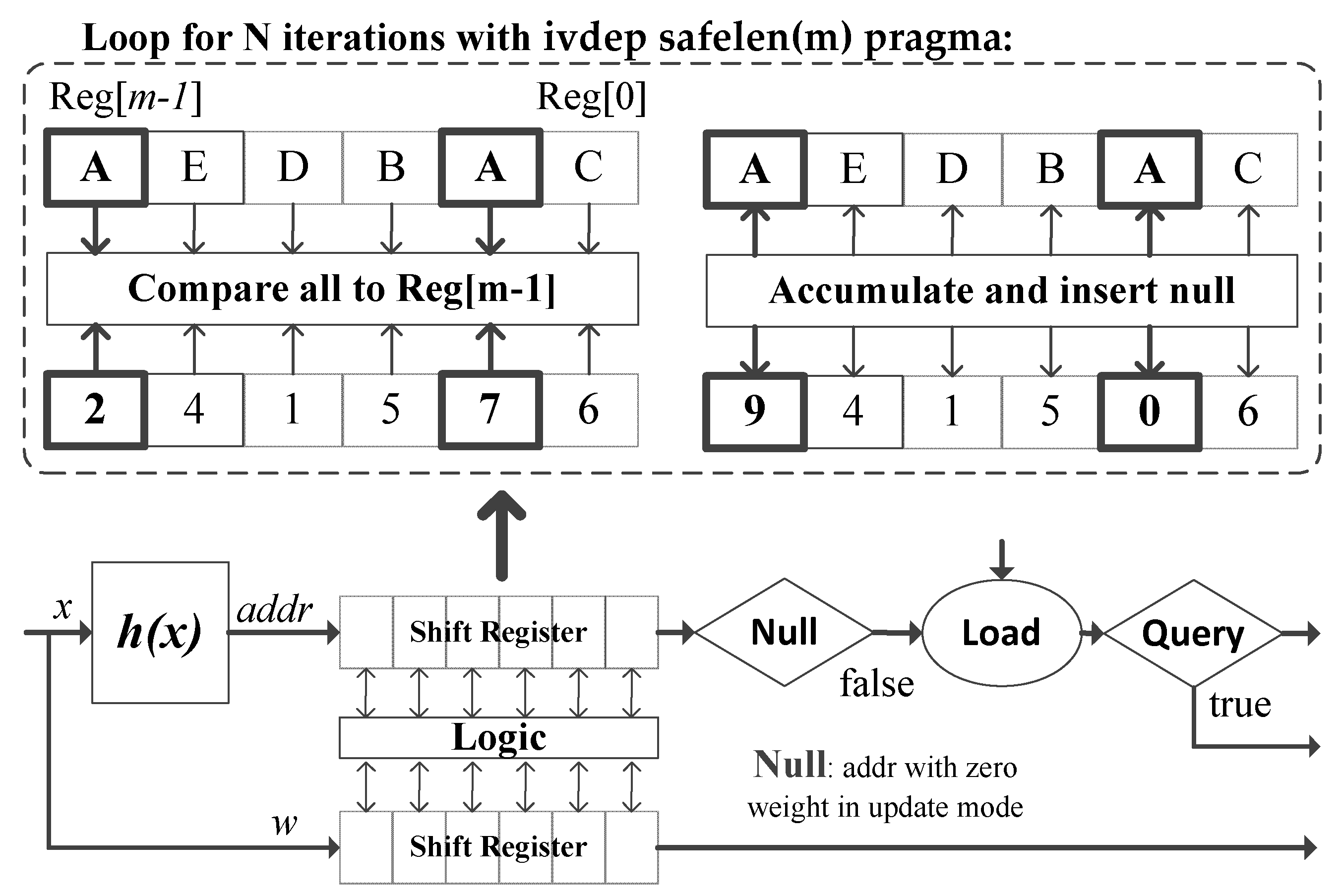
5.1. Effect of Relaxing Memory Dependency

HLS tools usually support high-level pragmas to relax memory dependencies in loops, giving the compiler more flexibility in scheduling load and store operations. Using these pragmas does not resolve memory dependency, so the designer needs to guarantee that no such dependency will occur to prevent functional failure. In Intel HLS, the “ivdep safelen(m)” pragma can be used with loops to tell the complier that no memory dependency will occur for at least m loop iterations. Using this pragma has a significant effect on the throughput of the hash table task in Figure 3. First, an ii of 1 is achievable if m is larger than the memory latency. Second, the HLS scheduler is able to schedule the load and store operation further apart in the pipeline, allowing for a higher maximum operating frequency (fmax). This is particularly important when the table in the task is large and composed of many blocks of the RAM primitives that could be physically distanced on the FPGA chip.
To study the effect of relaxing memory dependency on the hash table task, three variants of this task were compiled using the Intel Arria 10 GX 1150 FPGA as a target. In the first variant the ivdep safelen(m) pragma was not used, whereas the safe length m was set to 4 and 8 in the second and third variants, respectively. The RAM word size, items and weights were fixed to 4 bytes. The size of the hash table t was varied from 215 to 219 (approximately 2.5% to 40% of the chip memory). The pipelining effort of the HLS compiler was set to meet the default target fmax of 240 MHz. No specific ii values were forced on the loops in the sketch, so, the compiler was free to select the best fmax-ii tradeoff. The achieved post-fit throughputs reported by the synthesis tools are shown in Figure 4. We can see the significant improvements possible by just relaxing memory dependency. The improvements were attributed to the lower ii and the higher achieved fmax. Experimenting with higher values of m did not achieve further improvements, as the feedback path to the RAM block did not seem to be the bottleneck any longer.
In [20], the authors experimented with scaling a similar hash table in a Xilinx Virtex UltraScale FPGA, using a simple optimization technique in RTL (see Section 3). Table 1 shows the drop in fmax when scaling the RAM block from 5% to 40% of the available on-chip RAM. We can see that the HLS-generated task scaled better than its RTL counterpart, even when partitioning the RAM to 64 pipelined blocks.

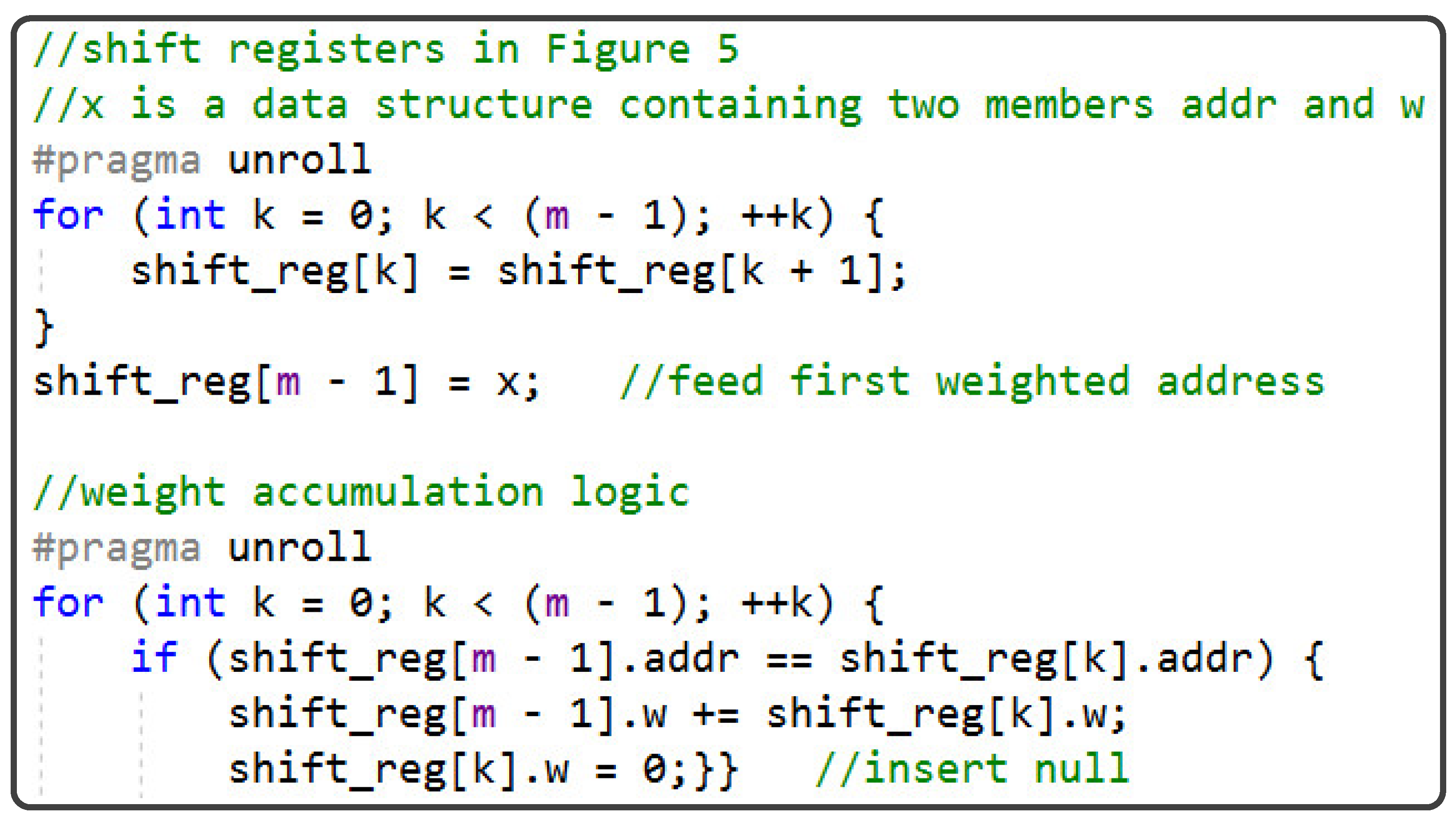
5.2. Pre-Update Weight Accumulation

As low-level access to the RAM ports is possible with RTL designs, several data forwarding techniques have been proposed to deal with the memory dependency issues [20,21,30]. To exploit the benefits of relaxing memory dependency in an HLS-generated sketch, we first need a high-level mechanism to break memory dependency in the hash table tasks. The HLS sketch in [27] deployed a “collector” circuit that stores a short history of the most recent memory updates in a small cache memory implemented using shift registers. Values from past updates are re-used in new updates to the same memory addresses. A similar approach was demonstrated in an Intel OneAPI kernel that computed the frequency histogram of a dataset [31]. Both approaches require the read and write ports of the sketch memories to be active all the time and they perform many redundant updates that could amount for most of the sketch updates when the stream is skewed, as will be seen in a later section.
A better and less complex solution based on Load-Store Queue (LSQ) architecture is presented in the modified hash table task shown in Figure 5. The solution requires the addition of a small observation window after the hash function stage. This window can be viewed as a pair of shift registers of size m with parallel-in parallel-out connections to some logic. One shift register takes the hashes of the items in the stream and the other takes the associated weights. The logic compares the hash in the first register to all the hashes ahead in the shift register. The weight of the first hash is then incremented by the weight of any identical hash ahead in the shift register, which is replaced with a zero weight. Any hash with a zero weight in update mode represents a bubble (labelled null in Figure 5), which is removed further in the pipeline before initiating memory load and store operations. Implementing pre-update weight accumulation in HLS is straightforward, as only two unrolled loops are required (see Figure 6). One loop represents a shift register, and the other loop represents the weight accumulation logic. The shift register is defined with a structure type encapsulating two members, the first being a memory update address, generated by the hash function, and the second the associated weight. The weight accumulation loop needs to be minimal to limit the critical path when m is increased.
By accumulating the weights backwards in the window, and ignoring the inserted bubbles, we effectively break the memory dependency for m iterations. The only difference in the invocation of a sketch component that deploys pre-update weight accumulation is the requirement to send an extra padding sequence with zero weights to flush the shift registers.
There is one safety issue that needs to be addressed when opting for the simple LSQ architecture in Figure 5. When flushing the shift register in a table task at the end of a sketch invocation in update mode, it is possible that one or more of the padding characters generate addresses that cause weights in the last m items in the stream to accumulate backwards and not update the tables in one or more table tasks. As m is generally small, and the hash function salts are generated offline, a simple and effective way around this issue is to flush the shift register with a unique padding sequence pre-calculated offline so that it guarantees that there would be no address collisions in any of the table tasks for at least m consecutive characters.
It is noted that an “aggregate” circuit similar to the LSQ in Figure 5 was implicitly suggested in [27]. However, it is not clear why it was not used in the sketch implementation. Perhaps, the deployment of the LSQ did not make a significant difference to the fmax of the small sketches used (t = 213).

5.3. Mixed Intiation Interval Design
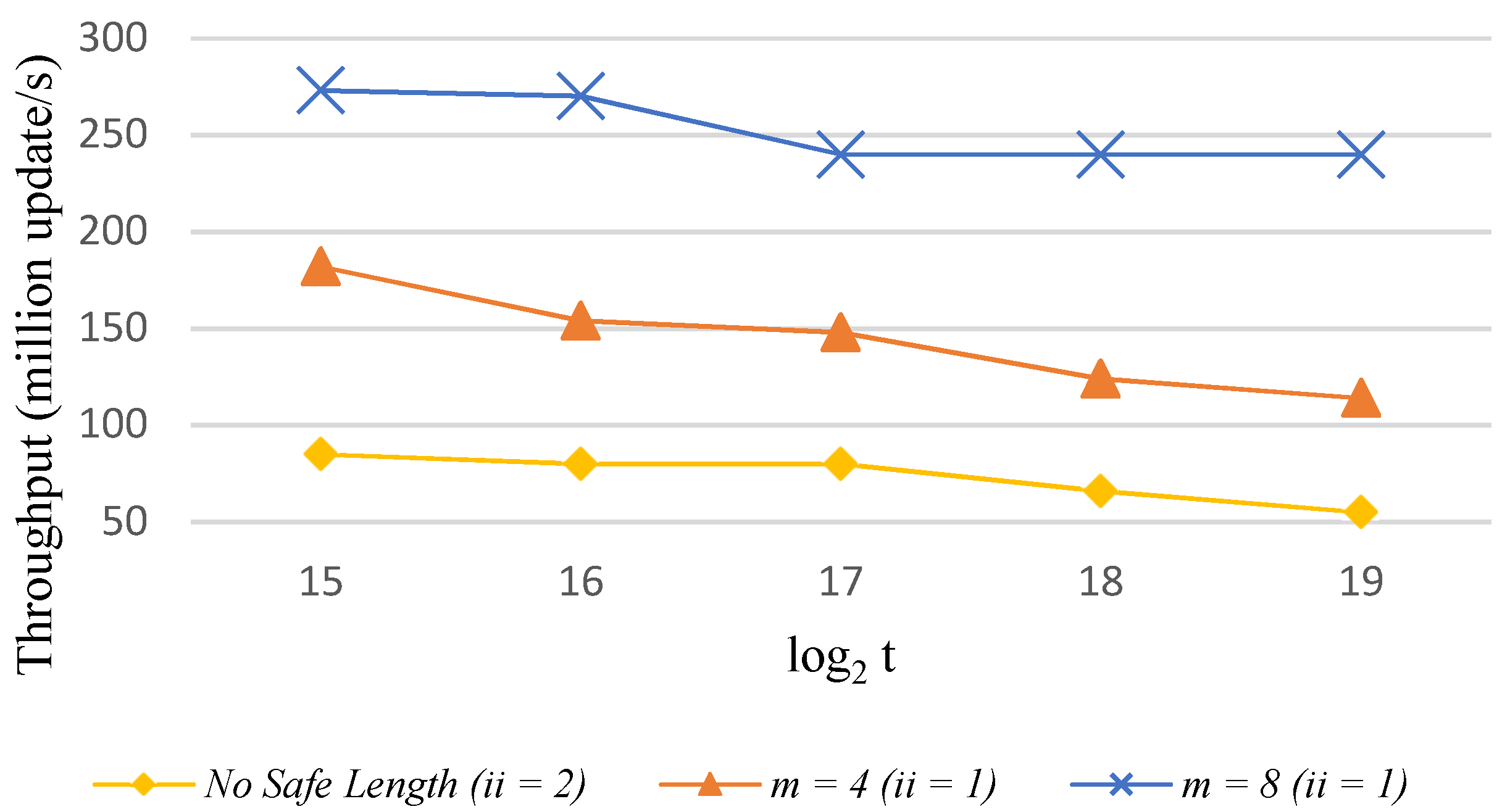
Most sketches presented in Section 3 are based on an “always run” model [1], meaning that the sketch does not have separate update/query functionality. Instead, the sketch continuously reads items from an input stream and writes count updates to an output stream for every item hit. While this model might be suitable for some applications, other applications may require a generic sketch approach with the flexibility to query items without updating the sketch. Consider for example a sketch accelerator paired with an embedded processor, which initiates Direct Memory Access (DMA) transfers from external memory to update the sketch. Intermittently, the processor initiates short transfers only to query some items of interest. As these queries are intermittent and short, the sketch throughput is only important when updating the sketch with stream data.
HLS tools allow users to specify certain ii values for the different hardware tasks in the design, provided that such values are achievable (example: table task in Figure 3 cannot achieve an ii of 1). In general, it is desirable to optimize an HLS design to achieve an ii of 1, as demonstrated with the pre-update weight accumulation technique. In some situations, users may want to increase the ii in some non-critical parts of the design to give the compiler more flexibility in scheduling the different operations in the pipeline. This can yield higher throughputs when higher target fmax is specified for the compiler. We can take advantage of this optimization when implementing a sketch following the separate update/query model (see Figure 7). By forcing an ii of 1 in the tasks invoked when updating the sketch and increasing the ii in the tasks only invoked for item queries (find-minimum in case of Count-Min sketch), stream update throughput can be increase at the expense of lower query throughput.

5.4. Evaluation

This section evaluates the presented throughput optimizations on a fully functioning Count-Min sketch constructed as a system of tasks (see Figure 2). The sketch complies with Intel FPGA standard interfaces and can be easily integrated with an Intel Avalon bus system. To evaluate the optimized sketch against the naïve implementation, the midrange Arria 10 GX 1150 FPGA was selected as a target device. This is the largest chip from the Arria 10 family with 427,200 Adaptive Logic Modules (ALMs), 1518 Digital Signal Processing (DSP) blocks and 2713 M20K embedded RAM blocks. The word size in the RAM blocks, the item and weight registers were all fixed to 4 bytes. The hash function parameters were generated offline and specified as constants at compile time.
First, the pre-update weight accumulation optimization technique was evaluated. Throughout the evaluation experiments, the compiler settings were kept at default (target fmax of 240 MHz, best fmax-ii tradeoff). Three sketch sizes that fit the target chip were used in the evaluation. The first with (d = 16, t = 216), the second with (d = 8, t = 217) and the third with (d = 4, t = 218). The safe distance was fixed to m = 8 in all optimized configurations. Table 2 reports the post-fit resource utilization results for the optimized sketches (the difference with the unoptimized sketches is negligible when m = 8). Table 3 compares the performance metrics of the optimized sketches to their unoptimized counterparts. We can see that with the optimization the sketch could achieve more than 3x the throughput. Furthermore, the latency of a single item query was smaller when calculated according to the achieved fmax.
To extract more throughput from the Arria 10 chip, a mixed ii design strategy with a higher target fmax of 400 MHz was evaluated. Table 4 shows the performance results for the sketch when relaxing the ii for the find-minimum task and specifying an ii of 1 for the table tasks. In general, the achieved update throughput was higher for all tested configurations. We can see that a higher throughput of up to 30% was achieved for the sketch configurations with (d = 8, t = 217) and (d = 4, t = 218). No significant gain was reported for the sketch configuration with 16 table tasks. Analysis of the compiler report revealed that in this configuration the find-minimum task was not a performance bottleneck.
It is noted that the optimizations evaluated in this section could be seamlessly applied to other FPGA HLS tools, such as Xilinx Vitis, as they only require basic pragma support (loop unrolling, constraining memory dependence distance and forcing certain loop initiation interval values). The benefit of achieving high throughput with minimal place-and-route effort could also be extended to platforms other than FPGAs, especially with recent industry trends in deploying technologies like structured Application Specific Integrated Circuits (ASICs) and embedded FPGAs (eFPGAs). Major FPGA vendors provide customers with the option to easily migrate their FPGA designs to special structured ASICs with properties between FPGAs and standard-cell ASICs. For example, the intel eASIC development flow allows for an FPGA design to be migrated to an eASIC device to achieve much higher performance, lower power consumption and lower unit cost [32].

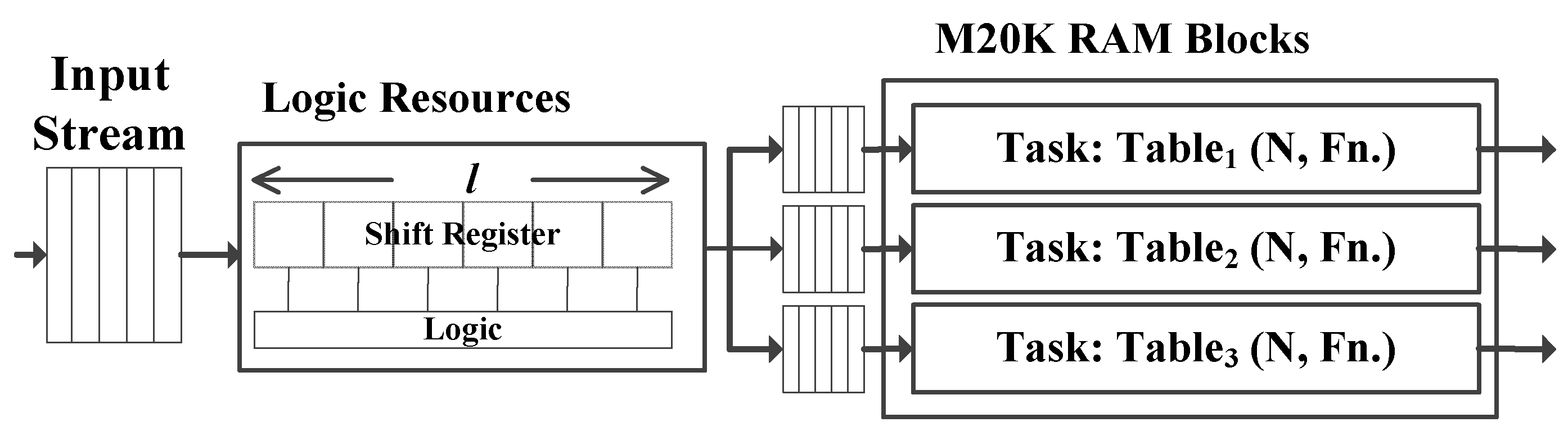
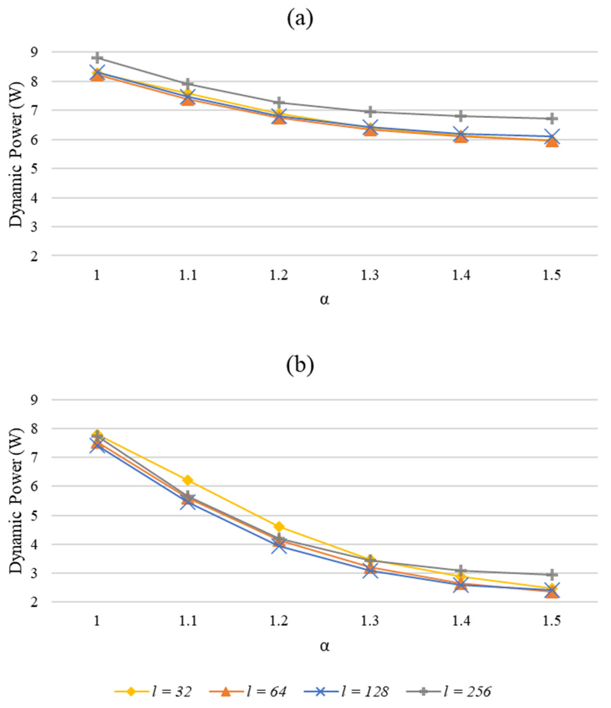
6. Optimizing for Low Power

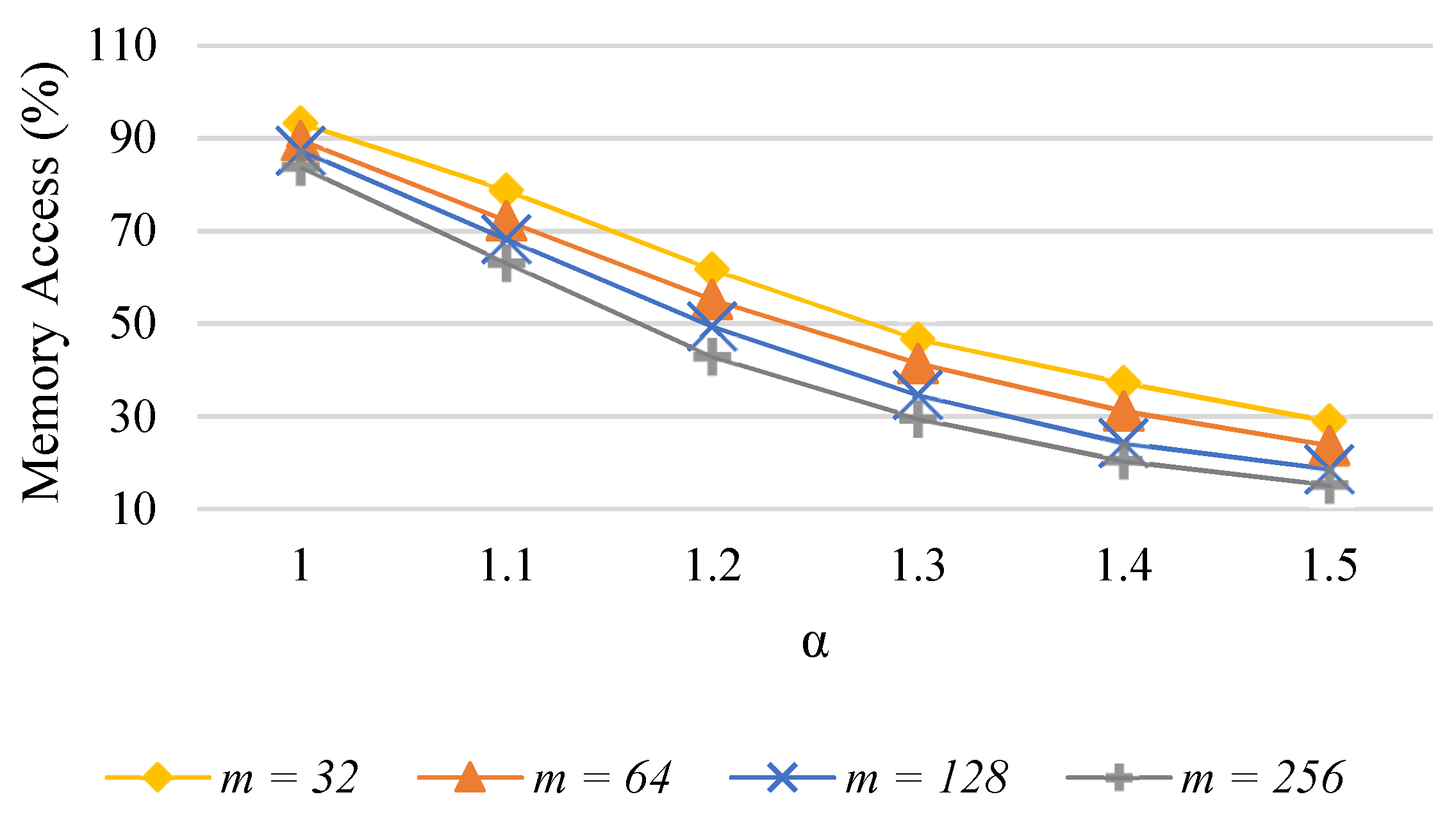
6.1. Reduced Memory Accesses in Skewed Streams

As discussed earlier, the primary use of pre-update weight accumulation is breaking memory dependency in the hash table tasks. In Section 5, test results showed that only a small memory dependency safe distance m was sufficient for achieving significant throughput gains, even for large sketches. The use of the pre-update weight accumulation technique could be extended to reduce the total number of memory accesses when processing the data stream. We could take advantage of the fact that data streams typically have a skewed frequency distribution. According to [33], many real-word streams can be modeled as heavily skewed Zipfian distributions [34]. By pre-counting item weights in the LSQ, significant reduction in total memory access rate is possible, as the bubble inserted in the pipeline would be removed before triggering memory load and store operations. This is particularly important in large sketches that are updated at high throughput as RAM is known to be a major contributor to the total dynamic power consumption in a typical FPGA system implementation.
Figure 8 evaluates the effect of pre-update weight accumulation on the memory access rate when different values of m are used. The reported results were calculated by simulation of synthetic input streams following a Zipfian distribution with Zipf parameter (α) values ranging from 1 to 1.5, without considering hash collisions. For moderately skewed inputs (α = 1), m had to be large to achieve reasonable reduction in memory access rate. For heavily skewed inputs, the reduction in memory access was significant, even for small values of m. Since, RAM is the dominant resource in a sketch, the optimization could be used to achieve significant reduction in total dynamic power consumption without loss in accuracy as in the stream filtering power optimization technique in [28].

6.2. Power Optimized Sketch

To capitalize on the possible reduction in total dynamic power consumption using pre-update weight accumulation, we can increase the safe length m inside each table task. However, this increases the area overhead, especially when the sketch parameter d is large. Also, when d and m have large values, any possible reduction in dynamic power can be offset by the power consumed by the LSQs. For reasonably small item sizes (say 32-bit integers), we can introduce a single accumulation window of size l at the input interface of the sketch, while keeping m small inside the hash table task (see Figure 9). The operation of this accumulation window is identical to the LSQ inside the hash table tasks; however, the window takes in the item identifiers rather than the hashes of the items. Flushing the shift register at the end of a sketch invocation in update mode is straightforward, as any padding sequence of unused item identifiers with zero weights is sufficient.

6.3. Evaluation

To evaluate the power optimized sketch, several configurations of the sketch were compiled with different values of l using the mixed ii compilation strategy and using an Arria 10 GX 1150 FPGA as a target device. Only l was varied in the different configurations of the sketch, all other parameters were fixed as: 32-bit items, m = 8, d = 4 and t = 218. The accumulation window length l was varied from 32 to 256 in four different configurations. In all configurations, the compiler achieved an fmax of at least 300 MHz. The RAM blocks in the hash table tasks were implemented as simple dual-port RAM (one port dedicated for reading and the other for writing), which consumed less power than true dual-port RAM.
Table 5 reports the dynamic power consumption estimates for the different sketch configurations obtained from the Intel FPGA early power estimation tool [35]. All configurations were assumed to operate at 300 MHz and assumed to process an input stream with a normal distribution, meaning that the window was unlikely to accumulate any weights and the RAM read and write ports were active all the time during streaming activity (the RAM read and write ports enable rate was set to 100% in the power estimation tool).
When processing skewed distributions, bubbles would be inserted in the pipeline by the accumulation window, as described in Section 5. Although these bubbles can theoretically eliminate the need for RAM read and write operations at the respective clock cycles, initial investigation of the HLS compiler generated source files suggested that the default RAM implementation internally enabled the ports of the RAM blocks, regardless of memory operations.
The limitation causing the RAM ports to be activated all the time is only related to the way the memory blocks are configured using the high-level wrapper files generated by the HLS tool. There is no low-level limitation in the FPGA RAM primitives preventing the deactivation of RAM operations in response to bubbles in the sketch pipeline. Therefore, it was worth studying the effect of deactivating the RAM operations on the dynamic power consumption of the sketch. Figure 10a shows the estimated reduction in dynamic power consumption caused by the recued RAM write operations in the optimized sketches when processing input streams modeled as Zipfian distribution with Zipf parameter (α) values ranging from 1 to 1.5. The power estimates were obtained from the Intel early power estimation tool after varying the write access rate in the tool according to the rates reported in Figure 8. We can see that the configuration with l = 64 performed slightly better than the other configurations, with an average reduction in dynamic power of 23% compared to the case of an input stream with a normal distribution. Figure 10b shows the dynamic power of the optimized sketches when deactivating both the RAM read and write operations in response to bubbles in the pipeline. We can see that the sketch configuration with l = 128 achieved an average reduction in dynamic power of 53%, compared to the case of an input stream with a normal distribution.
It is noted that the power analysis in this section was based on early rough estimates that demonstrated the potential benefit of the pre-update weight accumulation technique on reducing the dynamic power consumption. In fact, the power saving using this technique can be further extended to exploit clock-gating optimization features in modern FPGAs [36]. For example, by implementing a weight accumulation window as a separate component in a separate clock domain that precedes the sketch, power saving can be extended by gating the entire sketch. This, however, requires structural modifications to the presented sketch that we left for future work.

7. Comparison with the State-of-the-Art

This section compares the HLS optimized Count-Min sketch to the most relevant FPGA Count-Min sketch implementations in the published literature. Table 6 compares the design details and features of the sketches selected for evaluation (all designed using RTL description languages apart from the HLS sketch in [27]). All these sketches did not support weighted updates and used hardware-friendly hash functions to reduce the area overhead and design complexity. The only sketches to support the error guarantee of Count-Min were the sketches in [20,21], as they used a pairwise-independent hash family and did not modify the algorithm behind Count-Min. The sketch in [23] was based on a well-known variant of Count-Min based on a conservative sketch update strategy that would update a table entry for an item hit only if the entry actually contained the current minimum count estimate for the item [37]. The sketch in [25] was a modified hardware-optimized variant of the Count-Min sketch with limited empirical accuracy evaluation.
All the previously published work, apart from the work in [20,21,27], did not explicitly mention how the data hazard issue was resolved. The sketches in [20,21] implemented similar data forwarding mechanisms that required the memory to be accessed all the time, regardless of the input distribution. Memory access was also 100% for the HLS sketch in [27] when the “collect” default data forwarding method was applied rather than the “aggregate” LSQ technique. The sketch in [23] exhibited reduced memory update operations, due the conservative update strategy deployed by the sketch.
Most of the sketches in Table 6 were implemented using high-end Xilinx UltraScale and UltraScale + FPGA devices. Since our work was based on Intel FPGA technology, the proposed sketch was re-implemented on a Stratix 10 FPGA for better throughput comparison. There were two sketch sizes that matched the largest sizes used in the RTL optimized hardware sketches in [20,21]. Parameter m was set to 16 and pre-update weight accumulation was not used at the input interface. The mixed ii compilation strategy was used with a target fmax of 600 MHz (ii = 1 for table tasks and ii = 2 for find-minimum task after compilation). Table 7 compares the performance of the proposed sketch to the sketches in previously published work. In particular, we compared the throughputs of the sketches, as well as the accuracy parameters, assuming that all sketches were applying strong pairwise-independent hash functions. The Count-Min sketch in [27] was excluded from the comparison, as it is a part of a parallel multi-sketch system with no report of fmax. Additionally, sketches with sub-par throughputs and very small size parameters were excluded from the comparison
We can see that the reported throughput of 495 M updates/s in the proposed sketch with size parameters (d = 14, t = 217) was faster than its fastest counterpart by 50%. Moreover, the proposed sketch with size parameters (d = 5, t = 217) achieved a similar throughput compared to the extensively fine-tuned sketch in [21]. In fact, according to the extensive experiments conducted in [21], the maximum possible fmax for any sketch implemented on an Intel Stratix 10 FPGA was near 500 MHz. It is noted that in the relevant publications of the sketches in Table 7, the throughputs were reported in bits/s and calculated by multiplying the update rate by the item size, or by the network packet size in sketches targeting networking applications.

8. Conclusions and Further Research

This paper presented high-level design optimizations to better scale HLS-generated frequency estimation sketch data stream summaries. The paper demonstrated how the optimizations can be used with the Intel “System of Tasks” HLS design flow to implement efficient sketches that utilize large portions of an FPGA chip. When opting for these optimizations to implement an FPGA sketch, the benefits can be summarized as follows:
(1)
Easier design entry for a range of frequency estimation sketches compared to RTL (the main optimization only requires the addition of a small circuit specified with two simple unrolled loops).
(2)
Achieving significant throughput and latency advantages compared to unoptimized sketches designed with HLS (more than threefold increase in throughput is achieved).
(3)
Extracting the best possible accuracy from a given chip with error guarantee that can be tailored to specific streams with minimal effort at the design level (sketches utilizing 80% of the FPGA were easily synthesized).
Another important benefit of the presented work is the possible reduction in power consumption, due to the reduction in memory accesses (bubbles being continuously inserted in the pipeline). With early power estimates, the dynamic power consumption was shown to be reduced when processing skewed data streams, which are typical in many real-world applications. Future work will address power optimizations and analysis in more detail. Different ideas that involve stream filtering, power-gating and working with multiple clock domains will be explored and evaluated.

Funding

This research received no external funding.

Institutional Review Board Statement

Not applicable.

Informed Consent Statement

Not applicable.

Data Availability Statement

Not applicable.

Conflicts of Interest

The author declares no conflict of interest.

References

  1. Babcock, B.; Babu, S.; Datar, M.; Motwani, R.; Widom, J. Models and issues in data stream systems. In Proceedings of the Twenty-First ACM SIGMOD-SIGACT-SIGART Symposium on Principles of Database Systems, Madison, WI, USA, 3–5 June 2002; pp. 1–16. [Google Scholar]
  2. Kfoury, E.F.; Crichigno, J.; Bou-Harb, E. An exhaustive survey on p4 programmable data plane switches: Taxonomy, applications, challenges, and future trends. IEEE Access 2021, 9, 87094–87155. [Google Scholar] [CrossRef]
  3. Muthukrishnan, S. Data streams: Algorithms and applications. Found. Trends Theor. Comput. Sci. 2005, 1, 117–236. [Google Scholar] [CrossRef]
  4. Gribonval, R.; Chatalic, A.; Keriven, N.; Schellekens, V.; Jacques, L.; Schniter, P. Sketching data sets for large-scale learning: Keeping only what you need. IEEE Signal Processing Mag. 2021, 38, 12–36. [Google Scholar] [CrossRef]
  5. Alon, N.; Matias, Y.; Szegedy, M. The space complexity of approximating the frequency moments. J. Comput. Syst. Sci. 1999, 58, 137–147. [Google Scholar] [CrossRef] [Green Version]
  6. Charikar, M.; Chen, K.; Farach-Colton, M. Finding frequent items in data streams. In Proceedings of the International Colloquium on Automata, Languages, and Programming, Eindhoven, The Netherlands, 30 June–4 July 2002; pp. 693–703. [Google Scholar]
  7. Cormode, G.; Muthukrishnan, S. An improved data stream summary: The count-min sketch and its applications. J. Algorithms 2005, 55, 58–75. [Google Scholar] [CrossRef] [Green Version]
  8. Intel® High Level Synthesis Compiler Pro Edition: User Guide. Available online: https://www.intel.com/content/www/us/en/docs/programmable/683456/21–4/pro-edition-user-guide.html (accessed on 26 June 2022).
  9. Bledaite, L. Count-Min Sketch in Real Data Applications. Available online: https://skillsmatter.com/skillscasts/6844-count-min-sketch-in-real-data-applications (accessed on 18 July 2022).
  10. Team, D.P. Learning with Privacy at Scale. Apple Mach. Learn. J. 2017, 1, 1–25. [Google Scholar]
  11. Apache Spark: CountMin Data Structure. Available online: https://spark.apache.org/docs/2.0.1/api/java/org/apache/spark/util/sketch/CountMinSketch.html (accessed on 18 July 2022).
  12. RedisBloom: Bloom Filters and Other Probabilistic Data Structures for Redis. Available online: https://github.com/RedisBloom/RedisBloom/ (accessed on 18 July 2022).
  13. Bustio-Martínez, L.; Cumplido, R.; Letras, M.; Hernández-León, R.; Feregrino-Uribe, C.; Hernández-Palancar, J. FPGA/GPU-based acceleration for frequent itemsets mining: A comprehensive review. ACM Comput. Surv. (CSUR) 2021, 54, 1–35. [Google Scholar] [CrossRef]
  14. Ebrahim, A.; Khalifat, J. Fast Approximation of the Top-k Items in Data Streams Using a Reconfigurable Accelerator. In Proceedings of the International Symposium on Applied Reconfigurable Computing, Virtual Conference, 29–30 June 2021; pp. 3–17. [Google Scholar]
  15. Ebrahim, A.; Khlaifat, J. An Efficient Hardware Architecture for Finding Frequent Items in Data Streams. In Proceedings of the IEEE International Conference on Computer Design (ICCD), Lake Tahoe, NV, USA, 23–26 October 2020; pp. 113–119. [Google Scholar]
  16. Sun, Y.; Wang, Z.; Huang, S.; Wang, L.; Wang, Y.; Luo, R.; Yang, H. Accelerating frequent item counting with FPGA. In Proceedings of the ACM/SIGDA International Symposium on Field-Programmable Gate Arrays, Monterey, CA, USA, 26–28 February 2014; pp. 109–112. [Google Scholar]
  17. Gololo, M.G.D.; Zhao, Q.; Amagasaki, M.; Iida, M.; Kuga, M.; Sueyoshi, T. Low-cost Hardware that Accelerates Frequent Item Counting with an FPGA. IEIE Trans. Smart Processing Comput. 2017, 6, 347–354. [Google Scholar] [CrossRef]
  18. Sha, M.; Guo, Z.; Wang, K.; Zeng, X. A High-Performance and Accurate FPGA-Based Flow Monitor for 100 Gbps Networks. Electronics 2022, 11, 1976. [Google Scholar] [CrossRef]
  19. Zhang, Y.; Liu, Z.; Wang, R.; Yang, T.; Li, J.; Miao, R.; Liu, P.; Zhang, R.; Jiang, J. CocoSketch: High-performance sketch-based measurement over arbitrary partial key query. In Proceedings of the ACM SIGCOMM 2021 Conference, Virtual Conference, 23–27 August 2021; pp. 207–222. [Google Scholar]
  20. Tong, D.; Prasanna, V.K. Sketch acceleration on FPGA and its applications in network anomaly detection. IEEE Trans. Parallel Distrib. Syst. 2017, 29, 929–942. [Google Scholar] [CrossRef]
  21. Kiefer, M.; Poulakis, I.; Breß, S.; Markl, V. Scotch: Generating fpga-accelerators for sketching at line rate. Proc. VLDB Endow. 2020, 14, 281–293. [Google Scholar] [CrossRef]
  22. Soto, J.E.; Ubisse, P.; Fernández, Y.; Hernández, C.; Figueroa, M. A high-throughput hardware accelerator for network entropy estimation using sketches. IEEE Access 2021, 9, 85823–85838. [Google Scholar] [CrossRef]
  23. Soto, J.E.; Ubisse, P.; Hernández, C.; Figueroa, M. A hardware accelerator for entropy estimation using the top-k most frequent elements. In Proceedings of the Euromicro Conference on Digital System Design (DSD), Virtual Conference, 26–28 August 2020; pp. 141–148. [Google Scholar]
  24. Saavedra, A.; Hernández, C.; Figueroa, M. Heavy-hitter detection using a hardware sketch with the countmin-cu algorithm. In Proceedings of the 2018 21st Euromicro Conference on Digital System Design (DSD), Prague, Czech Republic, 29–31 August 2018; pp. 38–45. [Google Scholar]
  25. Sateesan, A.; Vliegen, J.; Scherrer, S.; Hsiao, H.-C.; Perrig, A.; Mentens, N. Speed records in network flow measurement on FPGA. In Proceedings of the 2021 31st International Conference on Field-Programmable Logic and Applications (FPL), Dresden, Germany, 30 August–3 September 2021; pp. 219–224. [Google Scholar]
  26. Tang, M.; Wen, M.; Shen, J.; Zhao, X.; Zhang, C. Towards memory-efficient streaming processing with counter-cascading sketching on FPGA. In Proceedings of the ACM/IEEE Design Automation Conference (DAC), Virtual Conference, 20–24 July 2020; pp. 1–6. [Google Scholar]
  27. Chiosa, M.; Preußer, T.B.; Alonso, G. SKT: A One-Pass Multi-Sketch Data Analytics Accelerator. Proc. VLDB Endow. 2021, 14, 2369–2382. [Google Scholar] [CrossRef]
  28. Singla, P.; Goodchild, C.; Sarangi, S.R. EHDSktch: A Generic Low Power Architecture for Sketching in Energy Harvesting Devices. In Proceedings of the 26th Asia and South Pacific Design Automation Conference, Virtual Conference, 18–21 January 2021; pp. 615–620. [Google Scholar]
  29. Kulkarni, A.; Chiosa, M.; Preußer, T.B.; Kara, K.; Sidler, D.; Alonso, G. Hyperloglog sketch acceleration on fpga. In Proceedings of the 2020 30th International Conference on Field-Programmable Logic and Applications (FPL), Gothenburg, Sweden, 31 August–4 September 2020; pp. 47–56. [Google Scholar]
  30. Preußer, T.B.; Chiosa, M.; Weiss, A.; Alonso, G. Using DSP Slices as Content-Addressable Update Queues. In Proceedings of the 2020 30th International Conference on Field-Programmable Logic and Applications (FPL), Gothenburg, Sweden, 31 August–4 September 2020; pp. 121–126. [Google Scholar]
  31. FPGA. Optimization Guide for Intel® oneAPI Toolkits. Available online: https://www.intel.com/content/www/us/en/develop/documentation/oneapi-fpga-optimization-guide/top.html (accessed on 26 June 2022).
  32. Intel Acquires eASIC—Why? Strategic Moves in the FPGA World. Available online: https://www.eejournal.com/article/intel-acquires-easic-why/ (accessed on 20 July 2022).
  33. Cormode, G.; Muthukrishnan, S. Summarizing and mining skewed data streams. In Proceedings of the 2005 SIAM International Conference on Data Mining, Newport Beach, CA, USA, 21–23 April 2005; pp. 44–55. [Google Scholar]
  34. Zipf, G.K. Human Behavior and the Principle of Least Effort; Addison-Wesley Press: Boston, MA, USA, 1949. [Google Scholar]
  35. Early Power Estimator for Intel® Arria® 10 FPGAs User Guide. Available online: https://www.intel.com/content/www/us/en/docs/programmable/683688/18–0-1/overview-of-the-early-power-estimator.html (accessed on 26 June 2022).
  36. Designing for Stratix 10 Devices with Power in Mind. Available online: https://www.intel.com/content/www/us/en/docs/programmable/683058/current/designing-for-stratix-10-devices-with.html (accessed on 26 June 2022).
  37. Goyal, A.; Daumé III, H.; Cormode, G. Sketch algorithms for estimating point queries in nlp. In Proceedings of the 2012 Joint Conference on Empirical Methods in Natural Language Processing and Computational Natural Language Learning, Jeju Island, Korea, 12–14 July 2012; pp. 1093–1103. [Google Scholar]
Figure 1. Count-Min sketch.
Electronics 11 02399 g001
Figure 2. The Count-Min sketch constructed using the Intel system of tasks HLS design flow.
Electronics 11 02399 g002
Figure 3. A naive hash table task implementation. The HLS compiler inserts stalling hazard protection logic at the RAM interface due to memory dependency.
Electronics 11 02399 g003
Figure 4. Effect of relaxing memory dependency by using the ivdep safelen(m) pragma in a hash table task (Arria 10).
Electronics 11 02399 g004
Figure 5. Breaking memory dependency in a hash table task using pre-update weight accumulation.
Electronics 11 02399 g005
Figure 6. Pre-update weight accumulation with loop unrolling.
Electronics 11 02399 g006
Figure 7. Raising target fmax in a mixed ii design can yield higher update throughput at the expense of lower query throughput.
Electronics 11 02399 g007
Figure 8. Memory access rate in a hash table task processing skewed synthetic data streams (Zipfian distribution).
Electronics 11 02399 g008
Figure 9. Power optimized sketch: pre-update weight accumulation with length l at the input stream interface.
Electronics 11 02399 g009
Figure 10. Dynamic power consumption estimates for a stream with a Zipfian distribution: (a) deactivating RAM write operations in response to bubbles in the pipeline, (b) deactivating both RAM write and read operations in response to bubbles.
Electronics 11 02399 g010
Table 1. Drop in fmax when scaling the RAM block from 5% to 40%.
OptimizationDeviceDrop in fmax
ivdep safelen(8) pragmaIntel Arria 1011%
RTL 64-stage pipeline [20]Xilinx Virtex UltraScale17%
RTL 32-stage pipeline [20]Xilinx Virtex UltraScale26%
RTL 16-stage pipeline [20]Xilinx Virtex UltraScale56%
Table 2. Chip utilization (Arria 10, m = 8).
Sketch FeatureChip Utilization (%)
tdɛ(1 − δ)ALMsDSPsM20K
216160.000030.9999818280
21780.0000150.99610180
21840.00000760.9450.580
Table 3. Performance (Arria 10, target fmax = 240 MHz).
tdOptimized?iifmax (MHz)Latency (ns) 1Throughput
(M Updates/s)
21616No215371277
2178No213979070
2184No212388662
21616Yes (m = 8)1255459255
2178Yes (m = 8)1232466232
2184Yes (m = 8)1234462234
1 Measured for a single item query at fmax.
Table 4. Performance (Arria 10, target fmax = 400 MHz).
tdOptimizationiifmax (MHz)Query Throughput
(M Updates/s)
Update Throughput
(M Updates/s)
21616m = 8, mixed ii1,2264132264
2178m = 8, mixed ii 1,2330165330
2184m = 8, mixed ii1,2312156312
Table 5. Dynamic power consumption estimates (Arria 10 GX 1150, normal distribution, f = 300 MHz, m = 8, d = 4 and t = 218).
Accumulation Window Length (l)Dynamic Power (W)
RAMLogicOthersTotal
327.030.700.948.67
647.030.741.008.77
1287.030.881.109.01
2567.031.321.309.65
Table 6. Sketch Comparison with Published Work.
SketchHash FunctionWeighted Updates?Error Guarantee?Memory Access (%)
ProposedEquation (1)YesYesvarious
[20]H3NoYes100%
[21]H3NoYes100%
[23]MurmurHashNoNovarious
[25]Xoodoo-NCNoNo100%
[27]MurmurHashNoNo100%
Table 7. Performance comparison with published work.
SketchDeviceSketch SizeAccuracy ParametersThroughput
(M Updates/s)
tdɛ(1 − δ)
ProposedStratix 10217140.0000150.99994494
ProposedStratix 1021750.0000150.97513
[20]Virtex UltraScale217140.0000150.99994325
[21]Stratix 1021750.0000150.97503
[23]UltraScale+ MPSoC21440.000120.94354
[25]Virtex UltraScale+21640.000030.94415
Publisher’s Note: MDPI stays neutral with regard to jurisdictional claims in published maps and institutional affiliations.

