Article

Characteristic Mode Analysis of a Ka-Band CPW-Slot-Couple Fed Patch Antenna with Enhanced Bandwidth and Gain

1
The School of Automation, Beijing University of Posts and Telecommunications, Haidian District, Beijing 100876, China
2
The School of Electronic Engineering, Beijing University of Posts and Telecommunications, Haidian District, Beijing 100876, China
*
Author to whom correspondence should be addressed.
Electronics 2022, 11(15), 2395; https://doi.org/10.3390/electronics11152395
Submission received: 7 July 2022 / Revised: 24 July 2022 / Accepted: 28 July 2022 / Published: 31 July 2022
(This article belongs to the Section Microwave and Wireless Communications)

Abstract

:
A Ka-band CPW-Slot-Couple (CSC) fed microstrip antenna with enhanced bandwidth and gain is presented in this paper. To simplify the feed network, the matching slots are designed at the end of the CPW. Consequently, the patch antenna is designed with a low profile, which has a size of 7.2 × 32.6 × 0.508 mm3. Characteristic mode analysis (CMA) is applied to illustrate the principle of the enhancement of the band with the form characteristic mode point of view. A slot based on inductive loading is employed on the parasitic patch to move the resonant frequency of CM3 to the resonant frequency of CM2 for enhanced bandwidth, which avoids introducing additional impedance matching networks. The measured results show that the bandwidth of the proposed monolayer antenna is 14.18% from 24.84 to 28.6 GHz and the peak gain is 7.9 dBi. Due to its attractive properties of low profile, compact configuration, wide band, and high gain, the proposed antenna could be applied to miniaturized millimeter-wave applications.

1. Introduction

As a significant part of the wireless communication system, the antennas are required to achieve greater bandwidth and gain to satisfy the rapid development and innovation challenges in emerging applications such as 5G mm-Wave communication, bio-radars, and defense application [1,2]. Microstrip patch antennas have the attractive merits of low profile and high integration, and they are extensively applied in Ka-band satellite communication, mobile communication, and other fields; however, the traditional simple single-layer mm-Wave patch antenna suffers from narrow operating bandwidth of less than 10% and low gain. Therefore, the application of broadband and gain-enhanced patch antenna has put forward high requirements, and various techniques emerge endlessly.
A traditional method is to adopt multi-layer structures, such as air cavity-backed, substrate integrated waveguide (SIW), and metasurface. In Ref. [3], the truncated square patch is excited by a SIW feedline with three layers of a printed circuit board (PCB), and another layer of the PCB with an air hole is designed for supporting and broadband. The fabricated prototype shows an impedance bandwidth of 19% covering 22.8 to 27.6 GHz, and a gain of 5.51 dBi. In Ref. [4], a pair of orthogonally arranged SIW is used to excite the metasurface. By doing so, insertion loss can be reduced, and impedance bandwidth can be expanded. Measured results show that the impedance bandwidth reaches 15.15% covering 23.8 to 27.7 GHz, and peak gain reaches 7.69 dBi. Although multi-layer structures are convenient to improve bandwidth and gain, it increases the size and the structural complexity of the antenna system.
To simplify the antenna structures, another method has been proposed and widely employed, which excites different modes of an antenna to enhance bandwidth and gain. The shorting pin or vias [5,6] are elaborately selected to excite multiple modes of a patch antenna, then the impedance matching network is configured to shorten the frequency points of the multi-mode and expand the frequency bandwidth. In Ref. [7], a circle of 10 shorting vias is designed in the air cavity to excite TM11 and TM13 modes. By configuring the impedance matching network, the TM11/TM13 and TM12/TM14 modes are selected to achieve a bandwidth of 6.46% and a peak gain of 15.1 dBi. Though this approach does not require a complex structure, it is not easy to realize multimode excitation at the operating frequency. Therefore, an impedance matching network is designed to adjust the input impedance, which will normally increase the quality factor of the antenna, and introduce some practical loss components.
To further enhance the bandwidth and gain of the patch antenna under low profile conditions, a Ka-band CPW-Slot-Couple (CSC) fed patch antenna with a single-layer structure is presented for the 5G mm-Wave application in this paper, as shown in Figure 1. The antenna has a thickness of 0.508 mm. Characteristic mode analysis (CMA) is applied to illustrate the principle of the enhancement of the band and gain. Slot based on inductive loading is employed on the parasitic patch to move the resonant frequency of CM3 to the resonant frequency of CM2 for enhanced bandwidth, which avoids introducing additional impedance matching networks. Simulation and optimization results show that the proposed antenna has achieved a bandwidth of 14.18% from 24.84 to 28.6 GHz and a maximum gain of 7.9 dBi. Due to its attractive properties of low profile, compact configuration, wideband and high gain, the proposed antenna could be applied to a 5G mm-Wave application.

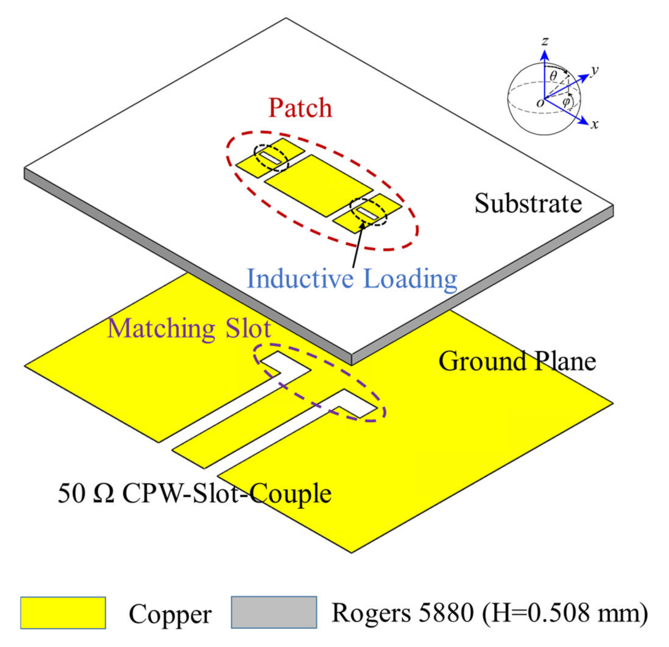
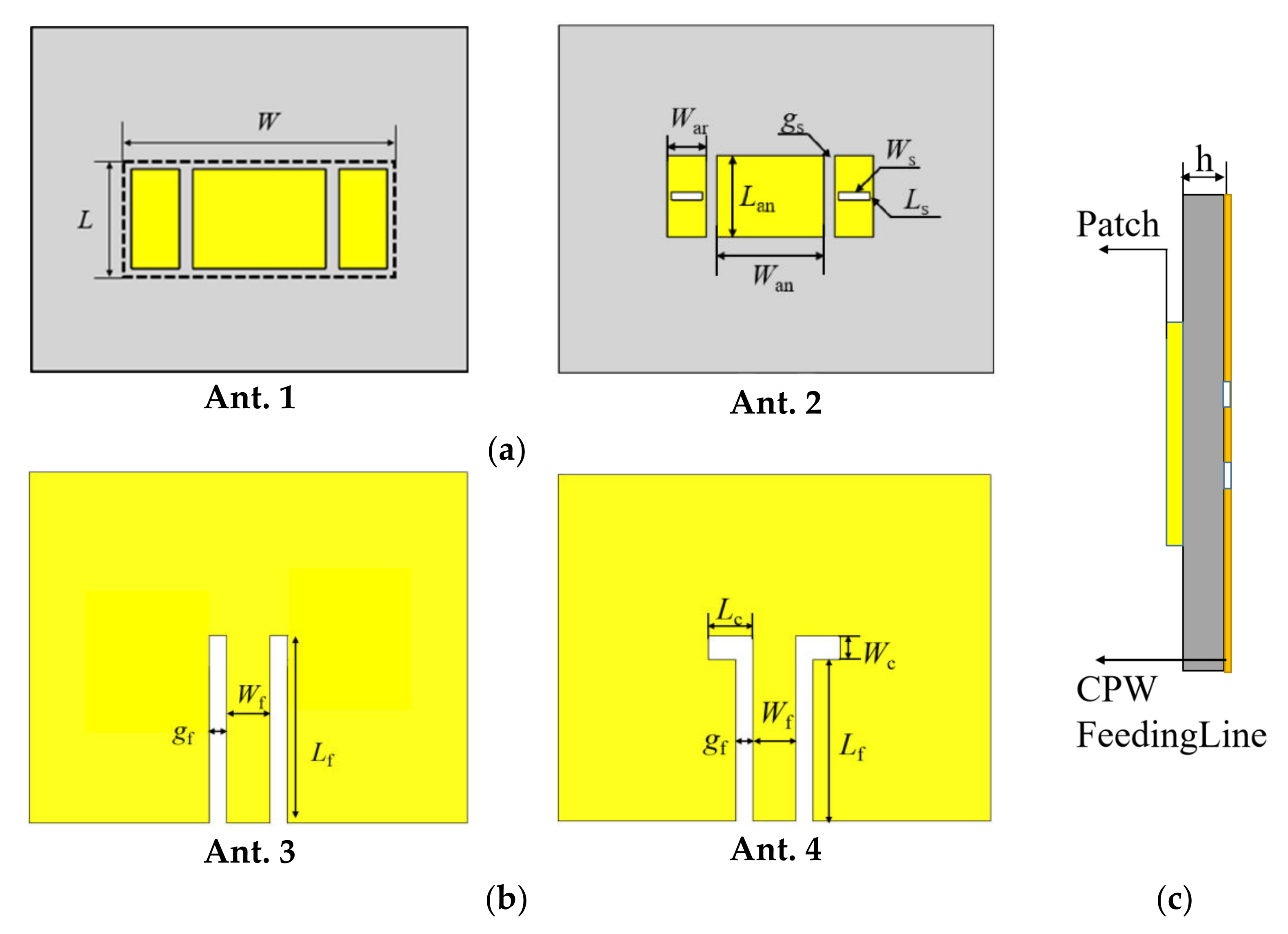
2. Antenna Design and Analysis

In this section, the design process of the proposed broadband and high gain antenna will be illuminated in detail. Then, the characteristic mode analysis is applied to illustrate the principle of the multi-mode excitation with the form characteristic mode point of view.

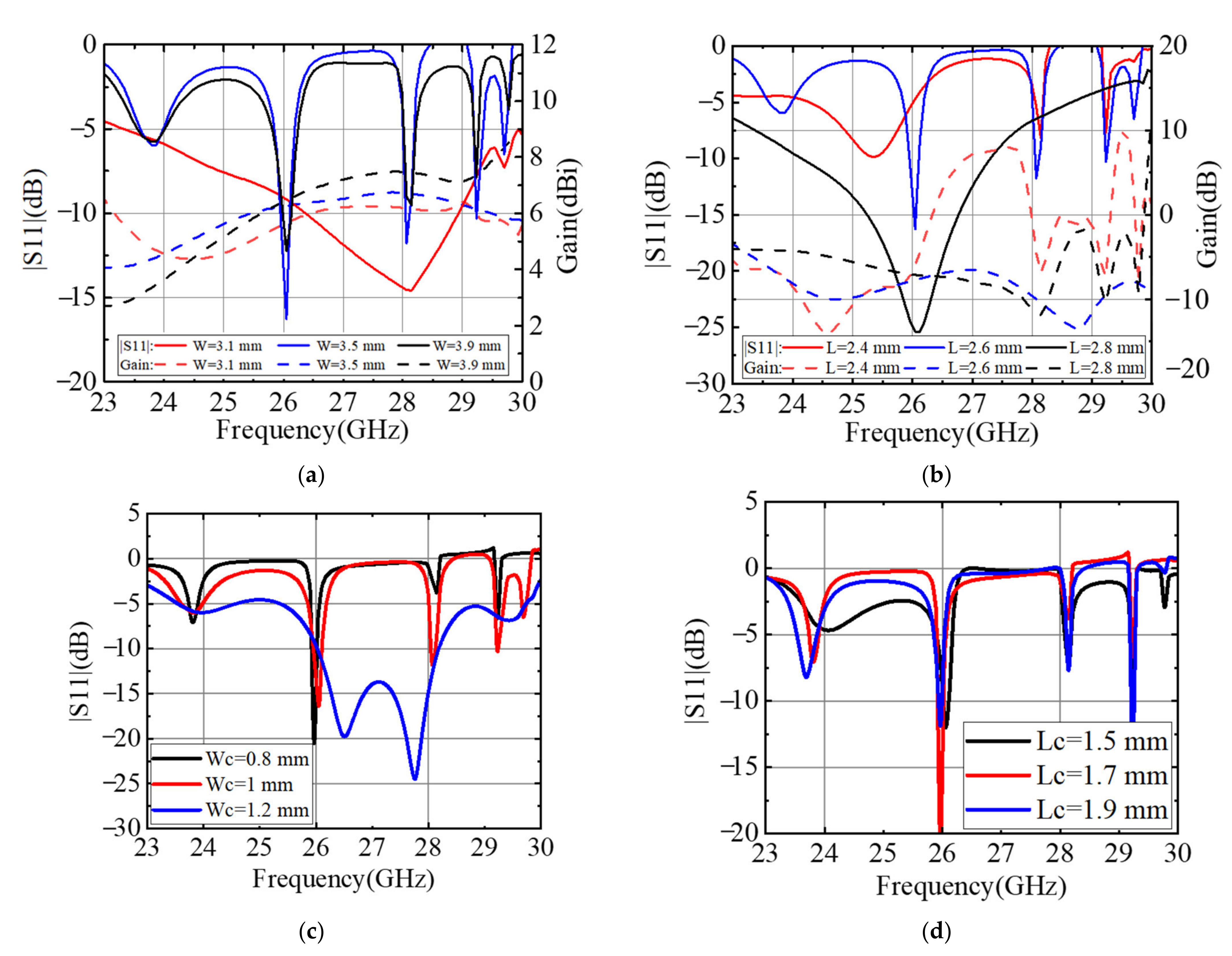
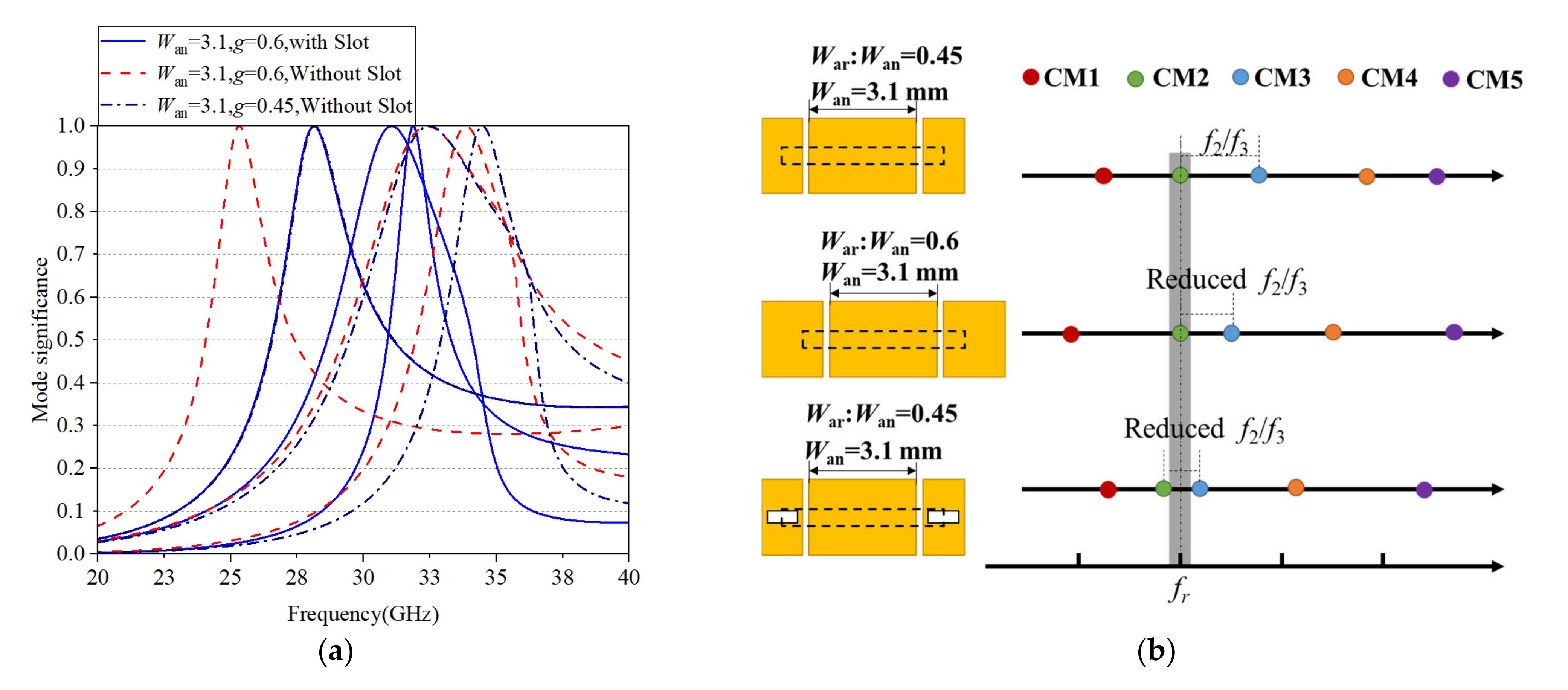
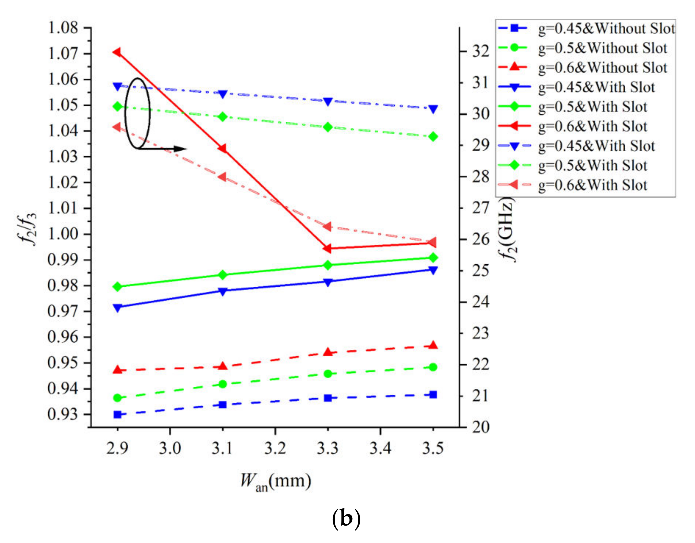
2.1. Antenna Configuration and Parametric Study

As shown in Figure 1, the proposed antenna is composed of a nonuniform patch on the top of a low dielectric constant high-frequency substrate (Rogers5880, h = 0.508 mm, εr = 2.2, tanδ = 0.0009) and a CPW-fed Coupling Slot at the bottom. Two matching slots are used to increase the coupling of the patch and the CPW-fed. The inductive loading on the patch is used for impedance matching, which can help enhance bandwidth and gain by shifting CM3 mode closed to CM2 mode. A Detailed characteristic mode analysis is carried out in the following section. The optimized parameters of the proposed antenna are shown in Table 1. ANSYS HFSS full-wave simulator is used to simulate the antenna performance.
Figure 2 illuminates the design process of the proposed antenna. Antenna 1 is composed of a nonuniform patch, and it’s excited by a slot-couple feeding circuit on the bottom, as shown in Figure 2a; however, the bandwidth of Ant. 1 is limited, two techniques, inductive loading and matching slots are applied on the foundation of Ant. 1 for bandwidth enhancement.
In Antenna 2, two slots based on inductive loading shown in Figure 2b are employed on the patch to move the resonant frequency of CM3 to the resonant frequency of CM2 for enhanced bandwidth, which avoids introducing additional impedance matching networks; moreover, the sizes of the sub-patches (War, Wan) and the gaps (gs) between them also contribute to the impedance matching. Detailed characteristic mode analysis is provided in Part B.
In Antenna 4, in order to enhance the antenna bandwidth, two matching slots were designed based on Antenna 3. The size of the matching slots (Wc × Lc) significantly impacts the impedance matching of high frequency.
Figure 3a illuminates the reflection coefficients and input impedance (Zin = Rin + jXin) of Ant. 4 in Figure 2. At the resonant frequency of the microship antenna, it may obtain Rin = 50 Ω and Xin = 0 [8]. As shown in Figure 3a, there is a resonant frequency at 27 GHz for the proposed antenna, which achieves well impedance matching. Figure 3b shows the simulated gain of Ant. 1 and Ant. 4 in Figure 2. Comparing the peak gain of the two antennas, Ant. 4 achieves a higher value of 8 dBi, and the introduction of two matching slots can enlarge the effective radiating aperture to increase the peak gain.
As shown in Figure 4, in order to further characteristic parameter analysis of the proposed antenna, the parametric studies of the width (W) and length (L), as well as the size of the matching slots (Wc × Lc) are carried out. Figure 4a,b show the |S11|and gain versus frequency for different W and L, respectively; it can be found in Figure 4a that decreasing W results in improved impedance matching near high frequency 28 GHz; conversely, it can be also seen from Figure 4b, the parameter L primarily impacts the impedance matching at low frequency 26 GHz; it can be considered that decreasing the width (W) and increasing the length (L) to expand the impedance bandwidth.
For microstrip antennas with well impedance matching, the gain is determined by the size of the radiating patch [9]. Therefore, only the W and L behavior of the peak gain for the proposed antenna is reported in Figure 4a,b; this figure shows that a gain larger than 8 dBi can be obtained by increasing the width (W) or decreasing the length (L).
Figure 4c,d illustrates that optimizing the size of the matching slots is beneficial to improving the coupling between the antenna and the underlying slot-couple feeding circuit. Increasing Wc results in improved impedance matching from 26 GHz to 28 GHz. As can be seen from Figure 4d, the parameter Lc primarily impacts the impedance matching for the high-frequency band.

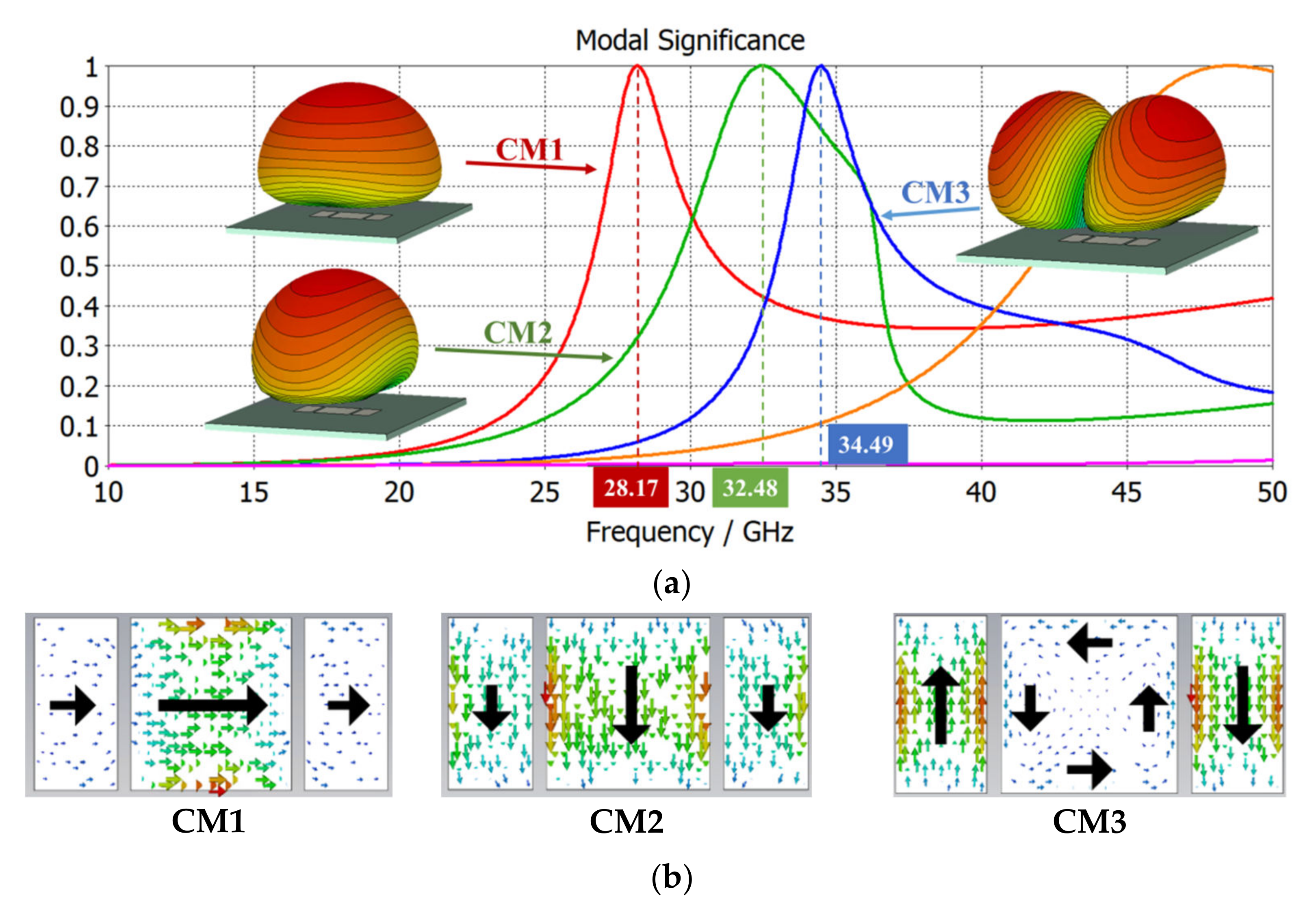
2.2. Characteristic Mode Analysis (CMA)

The mechanism of the multi-mode excitation antenna can be explained by the CMA [10,11]. In the CMA theory, the mutually orthogonal characteristic currents (Jn) are defined to describe orthogonal far-field radiation patterns. The surface current (J) of a conductor can be expressed as the sum of all characteristic currents:
J = n = 1 α n J n
X J n = λ n R J n
where αn is the modal weighting coefficient (MWC) of the n-th CM current, [X] is the imaginary part and [R] is the real part of the impedance matrix [12].
At the resonance point, the radiated energy of the antenna is the largest, and the eigenvalue ( λ n ) is zero. The n-th MWC can be determined by Equation (3) with λ n the n-th characteristic eigenvalue equation:
α n = J n , E t a n i 1 + j λ n
where E t a n i is the tangential electric field on the surface of the conductor. The significant parameters of modal significance (MS) and modal excitation coefficient (MEC) are shown in Equations (4) and (5).
MS = 1 1 + j λ n
MEC = J n , E i
A new set of eigenvalues, un, is defined when reactive elements [XL] are loaded in the conductor, which is equivalent to introducing an impedance matching network, the equivalent circuit is shown in Figure 5.
X + X L J n = u n R J n
u n = λ n + X L [ R ] 1
where un can be dominated by the reactive loading as shown in Equation (8):
X L = 2 π f L ( X L > 0 ) 1 2 π f C ( X L < 0 )
From Equations (6) to (8), by loading inductive and capacitive elements to adjust the impedance matching, the resonant frequency of the characteristic model can be moved to a lower or higher frequency.
Figure 6a shows the MS, radiation pattern, and modal surface current of the microstrip patch antenna. The required CM currents are selected by the MS values, and they can be moved to a lower or higher frequency by loading inductive and capacitive elements. Normally, when the MS value is higher than 0.7, the represented mode has the potential to radiate efficiently [13]. As seen in Figure 6a, the MS of CM3 mode is greater than 0.7 from 33 to 36 GHz, while the CM2 mode reveals a much wider impedance bandwidth, from 30 to 36 GHZ. If the modes of CM2 and CM3 are excited simultaneously, the bandwidth could be extended effectively. In consequence, the proposed principle of multi-mode excitation is equivalent to shifting CM3 mode closed to CM2 mode from the view of characteristic mode.
In order to enhance the bandwidth of the antenna, a higher-order characteristic mode can be moved to the lower desired characteristic mode by an inductively coupled excitation (ICE) structure, such as a slot or small circle. As shown in Figure 7, for the proposed antenna, the resonant frequency of CM2, f2, is used as operating frequency fr, and the ratio of f2/f3 can be reduced by increasing the width ratio of the parasitic patch and main patch, War:Wan, or loading inductive slot on the parasitic patches. As the frequency ratio of f2/f3 is reduced by increasing the width ratio of War:Wan, the basic mode CM2 will progressively approach the high-order modes in operating frequency, which also increases the antenna size. Therefore, under miniaturization conditions, loading an inductive slot with a suitable width ratio of War:Wan is the best solution.
To elucidate this issue in more depth, the width of the main patch, width ratio of g (g = War:Wan), and inductive slot are further analyzed for the characteristics mode of the proposed patch antenna, as shown in Figure 8. The fundamental size of Wan belongs to (0.3–0.4)λ0, where λ0 is the wavelength of 30 GHz; it can be seen that the frequency ratio f2/f3 gets closer to 1 with Wan increasing. Therefore, the two modes are easy to be excited simultaneously in widthband design. The peak value of frequency ratio f2/f3 varies with g, and it is optimal when g is between 0.6 and 0.8. As shown in Figure 8b, the frequency ratio of f2/f3 get increased when loading the inductive slot on the parasitic patch, and as Wan increase to 3.5 mm and g increase to 0.6, the frequency of f2 drops to 26 GHz.

3. Simulation and Measured Results

In this section, the proposed antenna has been simulated, fabricated, and measured to show its performance. Figure 9a shows the top and bottom views of the fabricated prototype, it’s composed of a nonuniform patch on the top of a low dielectric constant high-frequency substrate (Rogers5880, h = 0.508 mm, εr = 2.2, tanδ = 0.0009) and a CPW-fed coupling slot at the bottom. The optimized parameters are given in Table 1. The S-parameter results are measured by the vector network analyzer (R&S ZVA50), and the radiation patterns are measured in an anechoic chamber, as shown in Figure 9b.

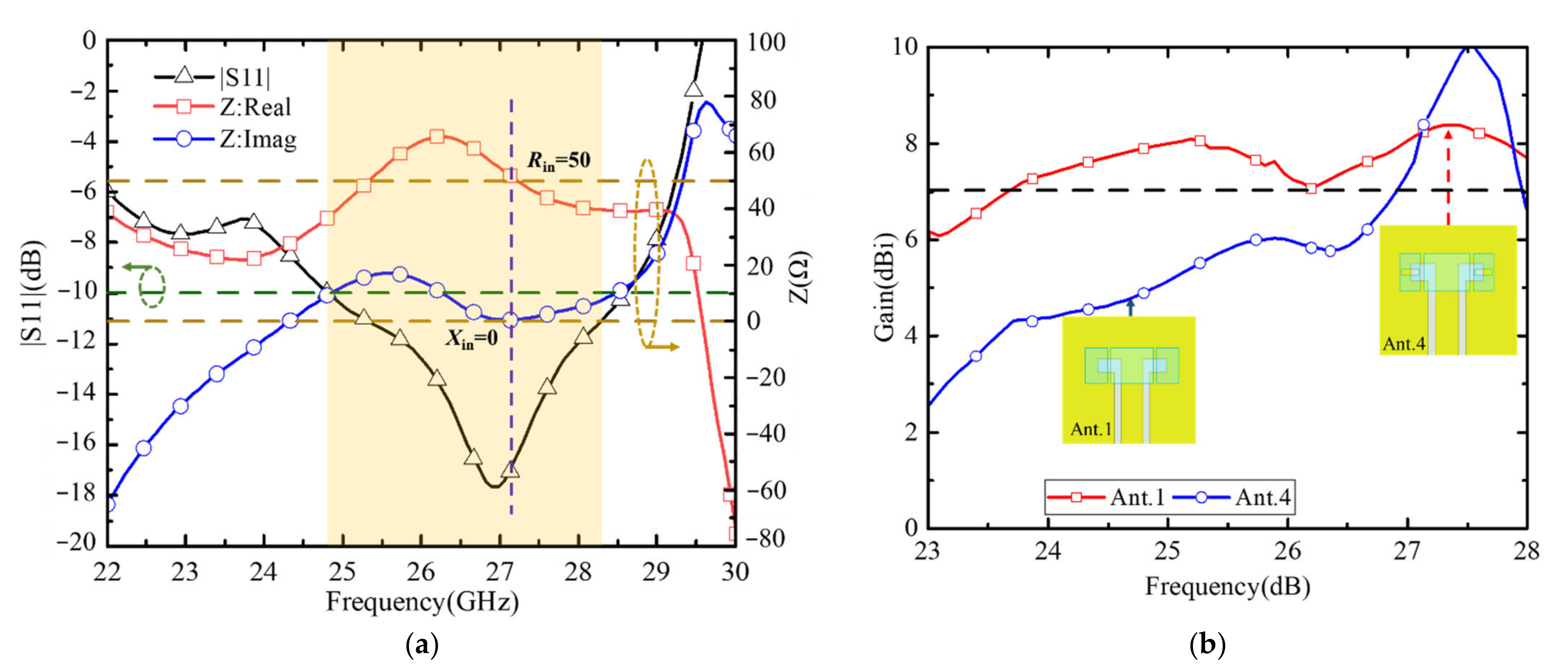
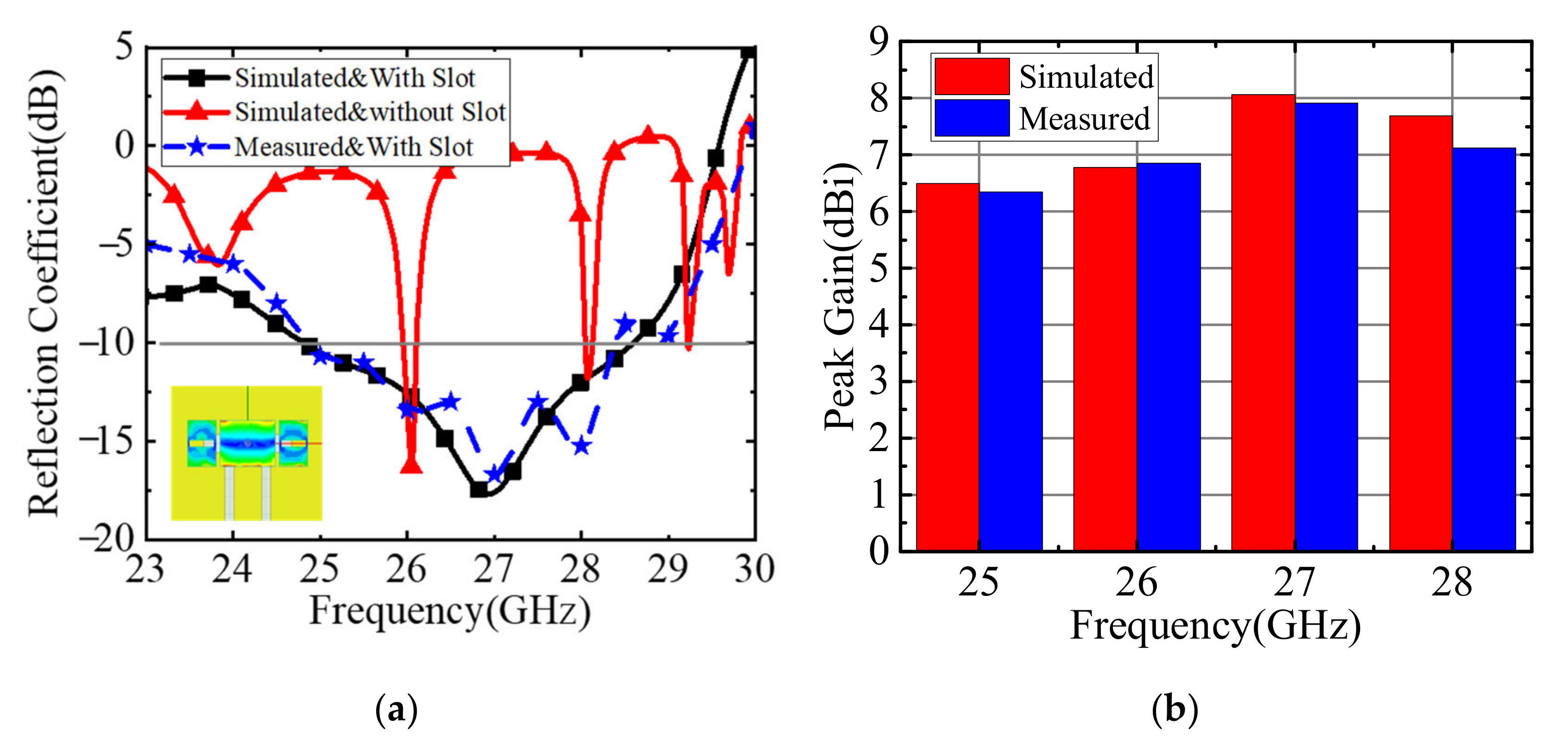
3.1. Impedance Bandwidth and Radiation Gain

The reflection coefficients of the proposed CPW fed patch antenna is depicted in Figure 10a; it is observed that the antenna without slot can excite multiple modes, however, the impedance matching (|S11| < −10 dB) of each mode is relatively poor. The measurement shows that the antenna with an inductive slot offers a good impedance matching for a wideband frequency starting from 24.84 to 28.6 GHz corresponds to a bandwidth of 14.18% with respect to the central frequency. Figure 10b shows the simulated and measured realized gain versus frequency. The measured peak gain is 7.9 dBi, the enhanced gain characteristics are thanks to the successful implementation of the nonuniform patch.

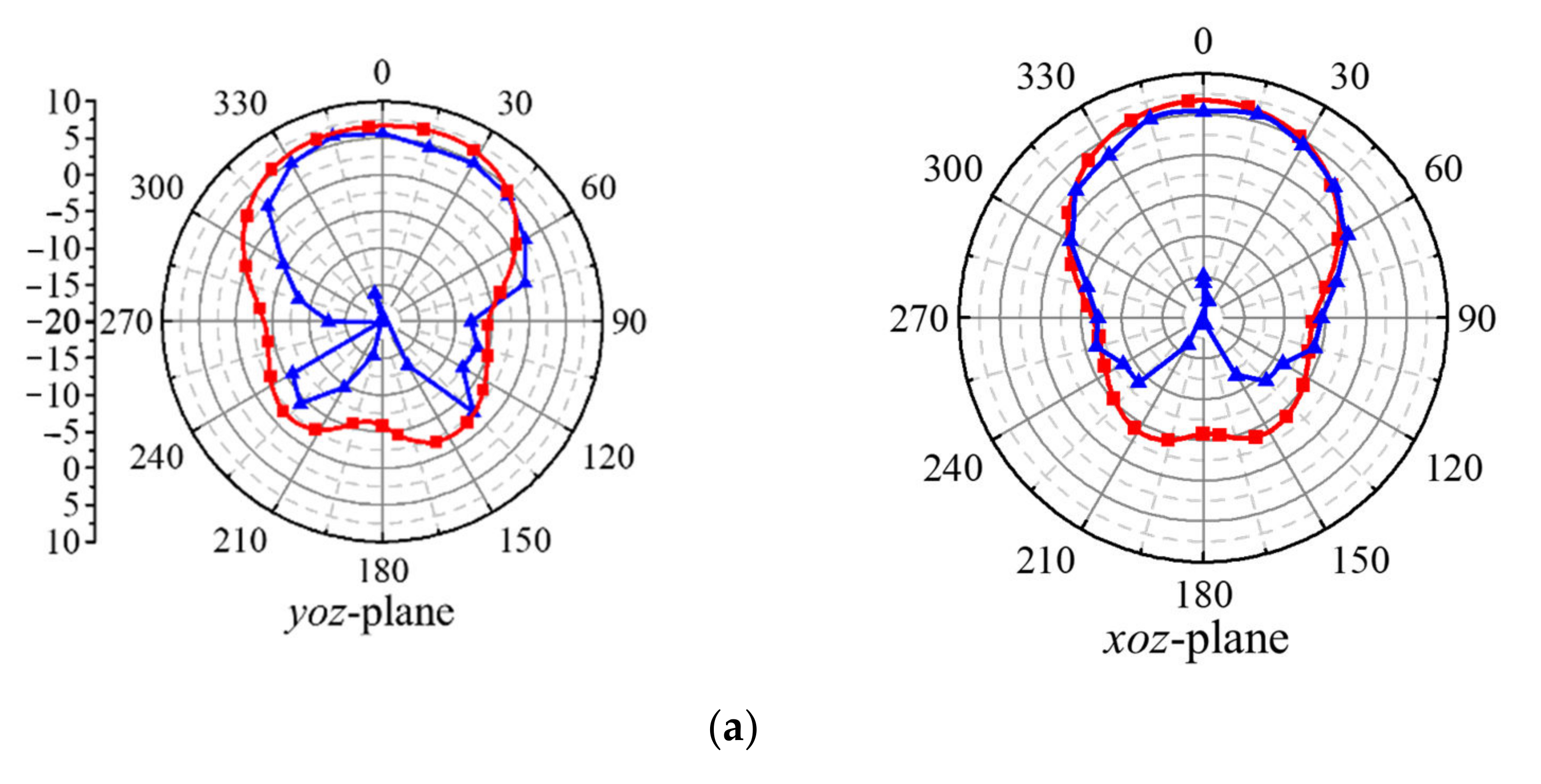
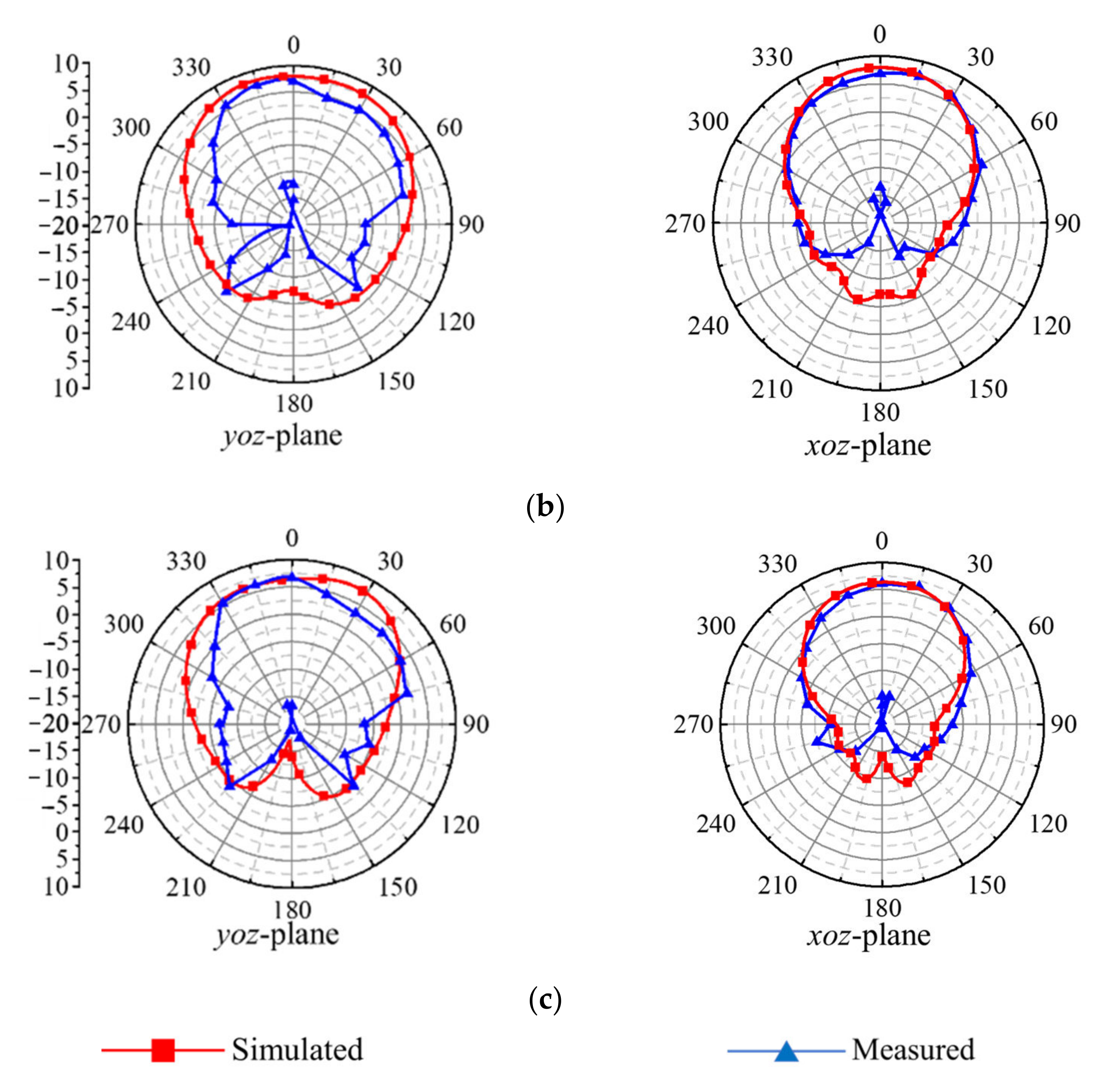
3.2. Radiation Patterns

Figure 11 displays the simulated and measured radiation patterns at 26, 27 and 28 GHz. The relatively low backward radiation is mainly due to the relatively closed CSC feed structure and ground. In the xoz-plane, the simulated results approximately coincide with the measured; however, in the yoz-plane, the measured radiation patterns are narrower compared with the simulated ones. The beamwidth and shape remained relatively steady in the band, and the half-power beamwidths (HPBWs) in the yoz-plane are 57.4°, 50.7° and 47.2° at 26, 27 and 28 GHz, while the corresponding HPBWs in the xoy-plane are 35.6°, 39.1° and 37.6°, respectively.

3.3. Comparison and Discussion

Table 2 is a comparison of the performance parameters between the proposed antenna and the other reported Ka-band patch antenna. The single-layer patch antenna based on shorting pin, SIW in Refs. [14,15,16,17] achieved high radiation efficiency and gain. Nevertheless, they suffer from narrow operating bandwidth of less than 10%. Different methodologies such as air cavity-backed [18], ESIW [19], SIGW [3] and metasurface [4,20] based on multilayer antenna structure were adopted in the designs with impedance bandwidth larger than 10%, but multilayer structure introduces additional losses resulting in a gain decrease of 1–3 dB. Furthermore, the air cavity-backed based, SIW-based, ESIW-based and metasurface-based patch antenna need to design complex feed networks to satisfy wideband impedance matching. As shown in Table 2, the proposed single layer CSC patch antenna exhibits merits of the relatively wide impedance of 14.18% from 24.84 to 28.6 GHz and the peak gain is 7.9 dBi, as well as a compact size of 7.23 × 2.6 × 0.508 mm3, ensuring that it is competitive in the mm-Wave 5G application.

4. Conclusions

In this paper, a Ka-band CSC excited microstrip patch antenna with broadband and high gain operating at multi-mode excitation has been presented. First, the size of the antenna is determined by the mode analyses, CSC is used to excite multiple modes of the antenna. Then, Characteristic mode analysis (CMA) is applied to illustrate the principle of the enhancement of the band with the form characteristic mode point of view, and a slot based on inductive loading is employed on a parasitic patch to move the resonant frequency of CM3 to the resonant frequency of CM2 for enhanced bandwidth, which avoids introducing additional impedance matching networks. Prototypes are finally designed, simulated and analyzed. The results show that the impedance bandwidth of the proposed monolayer antenna is 14.18% from 24.84 to 28.6 GHz and the peak gain is 7.9 dBi, which is better than the reported antenna. Due to its attractive properties of low profile, compact configuration, wideband and high gain, the proposed antenna could be applied to 5G mm-Wave application.

Author Contributions

K.D. and J.Z. participated in the structure design and optimization, data analysis, simulation and measurement; Y.W. and K.H. participated in background research and feasibility analysis; F.Y. and C.L. provided assistance for writing and revision of the paper. All authors have read and agreed to the published version of the manuscript.

Funding

The project was supported by Fund of State Key Laboratory of Information Photonics and Optical Communications (Beijing University of Posts and Telecommunications) (No. IPOC2021ZT20), China.

Institutional Review Board Statement

Not applicable.

Informed Consent Statement

Not applicable.

Conflicts of Interest

The authors declare no conflict of interest.

References

  1. Yin, J.; Wu, Q.; Yu, C. Broadband Symmetrical E-Shaped Patch Antenna with Multimode Resonance for 5G Millimeter-Wave Applications. IEEE Trans. Antennas Propag. 2021, 67, 4474–4483. [Google Scholar] [CrossRef]
  2. Khan, M.; Chowdhury, M. Analysis of Modal Excitation in Wideband Slot-Loaded Microstrip Patch Antenna Using Theory of Characteristic Modes. IEEE Trans. Antennas Propag. 2020, 68, 7618–7623. [Google Scholar] [CrossRef]
  3. Ma, C.; Ma, Z.H.; Zhang, X. Millimeter-Wave Circularly Polarized Array Antenna Using Substrate-Integrated Gap Waveguide Sequentially Rotating Phase Feed. IEEE Antennas Wirel. Propag. Lett. 2019, 18, 1124–1128. [Google Scholar] [CrossRef]
  4. Feng, B.; He, X.; Cheng, J.C. Dual-Wideband Dual-Polarized Metasurface Antenna Array for the 5G Millimeter Wave Communications Based on Characteristic Mode Theory. IEEE Access 2020, 8, 21589–21601. [Google Scholar] [CrossRef]
  5. Liu, P.; Zhu, X.W.; Zhang, Y. Patch Antenna Loaded with Paired Shorting Pins and H-shaped Slot for 28/38 GHz Dual-band MIMO Applications. IEEE Access 2020, 8, 23705–23712. [Google Scholar] [CrossRef]
  6. Zhang, X.; Tan, T.; Wu, Q.S. Pin-Loaded Patch Antenna Fed with a Dual-Mode SIW Resonator for Bandwidth Enhancement and Stable High Gain. IEEE Antennas Wirel. Propag. Lett. 2021, 20, 279–283. [Google Scholar] [CrossRef]
  7. Squadrito, P.; Zhang, S.; Pedersen, G.F. Wideband or Dual-Band Low-Profile Circular Patch Antenna with High-Gain and Sidelobe Suppression. IEEE Trans. Antennas Propag. 2018, 66, 3166–3171. [Google Scholar] [CrossRef]
  8. Liu, N.W.; Zhu, L.; Choi, W.W.; Zhang, J.D. A low-profile aperture-couple microstrip antenna with enhanced bandwidth under dual resonace. IEEE Trans. Antennas Propag. 2017, 65, 1055–1062. [Google Scholar] [CrossRef]
  9. Balanis, C.A. Antenna Theory: Analysis and Design; Wiley-Interscience: Hoboken, NJ, USA, 2005; pp. 15–64. [Google Scholar]
  10. Vogel, M.; Gampala, G.; Ludick, D.; Jakobus, U.; Reddy, C.J. Characteristic Mode Analysis: Putting Physics back into Simulation. IEEE Antennas Propag. Mag. 2015, 57, 307–317. [Google Scholar] [CrossRef]
  11. Kim, D.W.; Nam, S. Systematic Design of a Multiport MIMO Antenna with Bilateral Symmetry Based on Characteristic Mode Analysis. IEEE Trans. Antennas Propag. 2018, 66, 1076–1085. [Google Scholar] [CrossRef]
  12. Kim, G.; Kim, S. Design and Analysis of Dual Polarized Broadband Microstrip Patch Antenna for 5G mm Wave Antenna Module on FR4 Substrate. IEEE Access 2021, 9, 64306–64316. [Google Scholar] [CrossRef]
  13. Yang, X.; Liu, Y.; Gong, S. Design of a Wideband Omnidirectional Antenna with Characteristic Mode Analysis. IEEE Antennas Wirel. Propag. Lett. 2018, 17, 993–997. [Google Scholar] [CrossRef]
  14. Yang, H.Y.; Hua, B. A Low-Cost, Single-Layer, Dual Circularly Polarized Antenna for Millimeter-Wave Applications. IEEE Antennas Wirel. Propag. Lett. 2019, 18, 651–655. [Google Scholar] [CrossRef]
  15. Cao, D.; Li, Y.; Wang, J. A Millimeter-Wave Spoof Surface Plasmon Polaritons Fed Microstrip Patch Antenna Array. IEEE Trans. Antennas Propag. 2020, 68, 6811–6815. [Google Scholar] [CrossRef]
  16. Chen, H.; Shao, Y.; Zhang, Y. A Millimeter Wave Triple-band SIW Antenna with Dual-sense Circular Polarization. IEEE Trans. Antennas Propag. 2020, 68, 8162–8167. [Google Scholar] [CrossRef]
  17. Pan, Y.M.; Qin, X.; Sun, Y.X. A Simple Decoupling Method for 5G Millimeter-Wave MIMO Dielectric Resonator Antennas. IEEE Trans. Antennas Propag. 2019, 67, 2224–2234. [Google Scholar] [CrossRef]
  18. Nai-Chen, L.; Jenn-Hwan, T. Double-Curved Metal in Multilayer Printed Circuit Boards for Bandwidth Enhancemen of Millimeter-Wave Patch Antennas. IEEE Trans. Antennas Propag. 2021, 11, 1088–1906. [Google Scholar]
  19. Khan, Z.U.; Loh, T.H.; Belenguer, A. Empty Substrate Integrated Waveguide Fed Patch Antenna Array for 5G mm-Wave Communication Systems. IEEE Antennas Wirel. Propag. Lett. 2020, 19, 776–780. [Google Scholar] [CrossRef]
  20. Xue, M.; Wan, W.; Wang, Q. Low-Profile Millimeter-Wave Broadband Metasurface Antenna with Four Resonances. IEEE Antennas Wirel. Propag. Lett. 2021, 20, 463–467. [Google Scholar] [CrossRef]
  21. Jin, H.; Luo, G.Q.; Wang, W. Integration Design of Millimeter-Wave Filtering Patch Antenna Array with SIW Four-Way Anti-Phase Filtering Power Divider. IEEE Access 2019, 7, 49804–49812. [Google Scholar] [CrossRef]
  22. Xu, J.; Hong, W.; Jiang, Z.H. Low-Profile Wideband Vertically Folded Slotted Circular Patch Array for Ka-Band Applications. IEEE Trans. Antennas Propag. 2020, 68, 6844–6849. [Google Scholar] [CrossRef]
  23. Huayan, J.; Wenquan, C.; Kousheng, C. Millimeter-Wave TE20-Mode SIW Dual-Slot-Fed Patch Antenna Array with a Compact Differential Feeding Network. IEEE Trans. Antennas Propag. 2018, 66, 456–461. [Google Scholar]
  24. Yang, C.; Yuandan, D. Wideband Circularly Polarized Planar Antenna Array for 5G Millimeter-Wave Applications. IEEE Trans. Antennas Propag. 2021, 69, 2615–2627. [Google Scholar] [CrossRef]
  25. Klionovski, K.; Sharawi, M.S.; Shamim, A. A Dual-Polarization Switched Beam Patch Antenna Array for Millimeter-Wave Applications. IEEE Trans. Antennas Propag. 2019, 67, 3510–3515. [Google Scholar] [CrossRef]
  26. Yang, S.J.; Pan, Y.M.; Shi, L.Y. Millimeter-Wave Dual-Polarized Filtering Antenna for 5G Application. IEEE Trans. Antennas Propag. 2020, 68, 5114–5121. [Google Scholar] [CrossRef]
Figure 1. Schematic topology of the CSC fed antenna.
Electronics 11 02395 g001
Figure 2. Configuration and geometrical parameters of the proposed antenna. (a) Top view; (b) Main view; (c) Lateral view.
Electronics 11 02395 g002
Figure 3. (a) The reflection coefficients and match the impedance of Ant. 4 in Figure 2; (b) Simulated gain of Ant. 1 and Ant. 4 in Figure 2.
Electronics 11 02395 g003
Figure 4. (a,b) The reflection coefficients and gain versus frequency for different W and L; (c,d) The reflection coefficients versus frequency for different Wc and Lc.
Electronics 11 02395 g004
Figure 5. Equivalent circuit model of the proposed antenna.
Electronics 11 02395 g005
Figure 6. (a) Simulated MS frequency responses of the antenna; (b) Surface current of CM1, CM2 and CM3.
Electronics 11 02395 g006
Figure 7. (a) Simulated MS frequency responses of the antenna; (b) Graphical demonstration of the antenna size and CMA; (c) Surface current of the antenna with slot.
Electronics 11 02395 g007aElectronics 11 02395 g007b
Figure 8. The frequency ratio of f2/f3 of the antenna with different size: (a) Different width ratio of g and Wan; (b) Different width ratio of g and with/without slot.
Electronics 11 02395 g008aElectronics 11 02395 g008b
Figure 9. (a) Configuration and geometrical parameters of the proposed antenna; (b) Antenna test scenario.
Electronics 11 02395 g009
Figure 10. (a) Comparison the simulated |S11| frequency responses of the antenna with/without slot. (b) Simulated gain of the proposed antenna.
Electronics 11 02395 g010
Figure 11. Simulated Phi = 0° and Phi = 90° radiation patterns of the proposed antenna. (a) 26 GHz; (b) 27 GHz; (c) 28 GHz.
Electronics 11 02395 g011aElectronics 11 02395 g011b
Table 1. Dimensional parameters of the proposed antenna.
ParametersValue (mm)ParametersValue (mm)
Wan3.1Wc1
War1.44Lc1.76
Lan2.6Wf1.578
Ws1.11Lf7.5
gs0.25gf0.5
Ls0.39
Table 2. Performance comparison of the proposed antenna with state-of-art works.
Refs.Printed LayersTechniquef0
(GHz)
−10 dB|S11|
BW (%)
Max. Gain (dBi)Antenna Size (mm3)
[14]1shorting pin306.57% (29.13–31.10 GHz)11.83.5 × 2.8 × 0.508
[15]1--283.4% (27.5–28.5 GHz)2.33.6 × 3.6 × 0.508
[16]1SIW & Shorting pin283.7% (27.46–28.5 GHz)6.930 × 15 × 0.3
[17]1Shorting pin267.3% (25.1–27.0 GHz)6.34.5 × 4.5 × 1.5
[18]2Air cavity-backed & coupled-feeding2922.1% (27.4–34.2 GHz)815 × 15 × 0.67
[19]2ESIW & Slot28.252.4% (26.5–30 GHz)122.6 × 4 × 1.016
[20]2Shorting pin & Metasurface2822% (24.4–30.5 GHz)6.5–1010 × 10 × 0.23
[21]2SIW285.03% (27.15–28.55 GHz)5.12.8 × 2.2 × 1
[22]2Coupled feeding29.3519.22%10.49·9 × 0.835×1.016
[23]2SIW2810%6.4825 × 25 × 1.16
[4]3SIW & Metasurface2515.15% (23.8–27.7 GHz)7.695.57 × 8.57 × 2.36
[24]3SIW & Shorting pin3044.62% (24.41–38.43 GHz)7.254.48 × 4.48 × 2.575
[25]3--28.719% (26–31.4 GHz)2.32.65 × 2.65 × 1.62
[26]5Parasitic patch2620% (24.26–29.5 GHz)56.8 × 6.8 × 1
[3]5SIGW&Air cavity-backed2619% (22.8–27.6 GHz)5.513.8 × 3.8 × 2.361
This work1CSC & Multi-mode2714.18% (28.6–24.84 GHz)7.97.23 × 2.6 × 0.508
Publisher’s Note: MDPI stays neutral with regard to jurisdictional claims in published maps and institutional affiliations.

