Article

A Fully Integrated Passive Self-Jamming Cancellation Architecture with Fast Settling Time for UHF RFID Reader

1
Research and Development Center of Healthcare Electronics, Institute of Microelectronics of Chinese Academy of Sciences, Beijing 100029, China
2
Beijing Key laboratory of RFIC Technology for Next Generation Communications, Institute of Microelectronics of Chinese Academy of Sciences, Beijing 100029, China
3
University of Chinese Academy of Sciences, Beijing 100049, China
*
Authors to whom correspondence should be addressed.
Electronics 2022, 11(15), 2311; https://doi.org/10.3390/electronics11152311
Submission received: 2 June 2022 / Revised: 16 July 2022 / Accepted: 19 July 2022 / Published: 25 July 2022

Abstract

:
This paper presents a fully integrated passive self-jamming cancellation (SJC) circuit in 0.18 µm Complementary Metal Oxide Semiconductor (CMOS) technology for ultra-high frequency (UHF) radio frequency identification (RFID) applications. Based on the active amplitude and phase control, a novel passive variable capacitor array and signal combiner are adopted instead of a traditional variable amplifier/attenuator and a phase shifter to reduce the circuit complexity and thus achieve higher linearity and low noise. We use an improved cancellation algorithm based on the local search method to quickly and accurately find the cancellation point that minimizes the self-jamming signal power. The simulation and measurement results are constant, and a suppression of 38 dB can be achieved in the working frequency of 860–960 MHz. The cancellation algorithm can be finished within 0.5 ms. These results indicate that the designed SJC circuit can be a promising candidate for UHF RFID applications.

1. Introduction

Ultra-high frequency (UHF) radio frequency identification (RFID) has received more attention due to its stronger anti-interference ability, longer transmission distance, etc. RFID realizes the identification and transmission of information using the spatial coupling of RF signals, which belongs to non-contact identification [1]. The RFID system consists of two parts: readers and tags. In the passive UHF RFID reader, the reader must transmit continuous waves (CW) to power up the tag while receiving the data sent by tags. For a single antenna reader, due to the limited isolation of the circulator or directional coupler, the CW signals transmitted by the reader will inevitably leak to the receiver (RX) [2], which is called a self-jamming signal. The power of the self-jamming signal is much greater than the useful signal received by the reader, so the useful signal will be completely submerged in the self-jamming signal, resulting in RX saturation and sensitivity reduction. The frequency of the self-jamming signal is close to that of the useful signal, so it is difficult to remove it by the filter. If self-jamming suppression is not applied, the low noise amplifier and mixer of the RF front-end must have a high dynamic range to correctly distinguish useful signals, which will undoubtedly increase the complexity of RF front-end design. At the same time, for the direct-conversion receiver, serious DC offset will occur after mixing the self-jamming signal with the local oscillator (LO) signal, which also poses a challenge to the design of the analog-to-digital converter (ADC). Therefore, the circuit structure with self-jamming signal suppression is of great significance in improving the performance of the RF front-end receiver of the UHF RFID reader.
In recent years, many transceiver systems based on UHF RFID readers have been manufactured [3,4,5,6,7]. Among them, some circuit structures [6,7] have been proposed to realize self-jamming signal suppression. Other works with only the SJC circuit are also proposed in [8,9,10,11,12,13,14,15]. In [8,9], impedance tuning circuits are added to the free port of the directional coupler, and cancellation is achieved by terminating the isolated port with a proper (reflective) impedance. Some use deformed microstrip rat-race circuits to replace the traditional circulator or directional coupler for better isolation [10]. These methods have the advantages of simple structure and low noise performance because the circuit is passive, but they are hard to be integrated and only work in a limited frequency range because of the narrowband filters.
Cancellation technologies using the replica of the transmitting carrier have been mentioned in [11,12,13]. They use an amplifier or attenuator to control the amplitude of the replica signal and use a phase shifter to control the phase [11,12]. However, the active circuits will produce thermal and phase noise in the SJC circuit, making the cancellation algorithm hard to converge. The architecture proposed in [13] completes the amplitude and phase control through the FPGA in the digital domain. However, it suffers from a long calibration time. Another proposed architecture [14] is achieved by comparing the leakage signal with the reference signal to determine the phase and amplitude difference using an RF gain and phase detector, which gives a better starting point for the search algorithm. However, the cancellation process also takes more than 20 ms to converge.
Based on the application of the UHF RFID transceiver, this paper proposes an SJC circuit, which uses a passive variable capacitor array and signal combiner to achieve phase and amplitude control. The phase and amplitude control circuits are composed of passive components, which feature low noise and high linearity compared to the active devices. We use the power detector to constantly detect the power of the self-jamming signal, and the proposed self-jamming cancellation algorithm realizes fast and stable control. The circuit has been fabricated in 180 nm CMOS technology, and the simulation results are demonstrated by measurements.
This paper is organized as follows: Section 2 gives the overall architecture of the UHF RFID transceiver and the proposed SJC circuit design issues. Section 3 demonstrates simulation and experimental results. Finally, Section 4 draws the conclusions of the entire work.

2. Analysis and Design

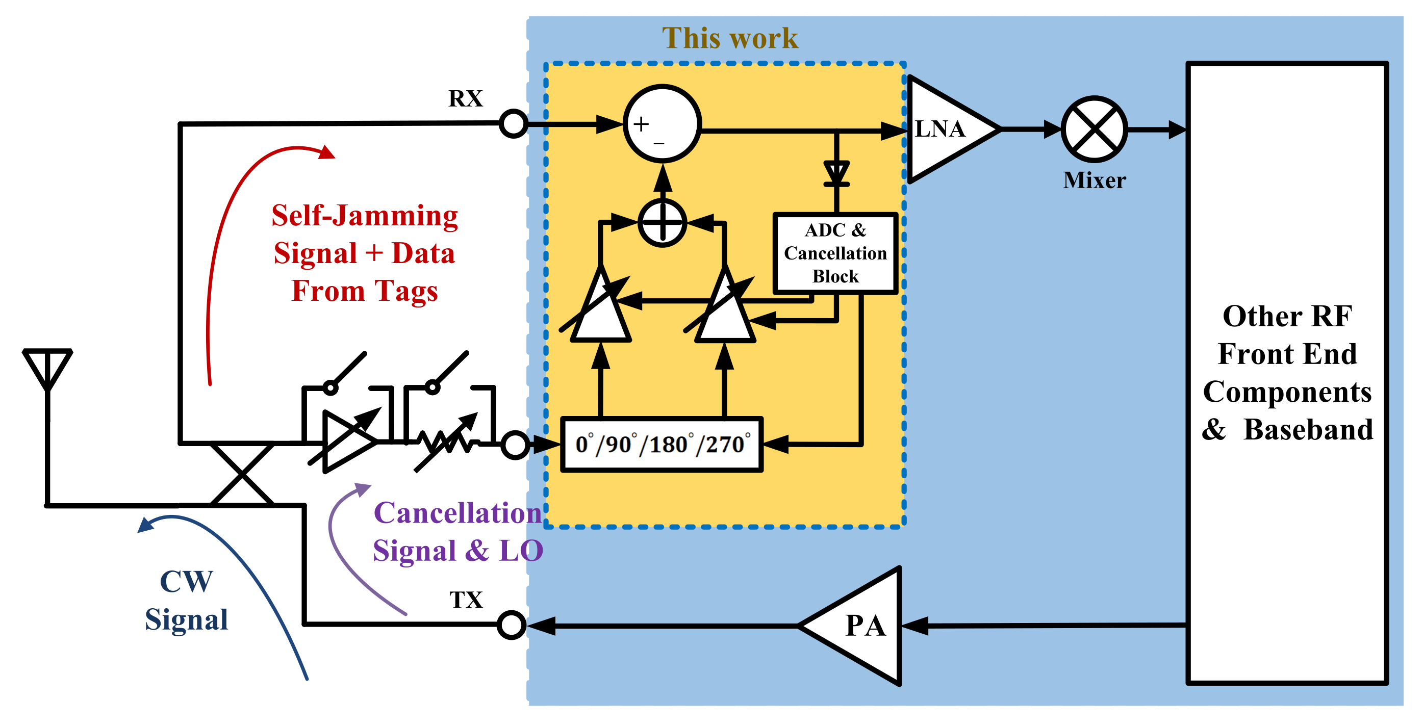
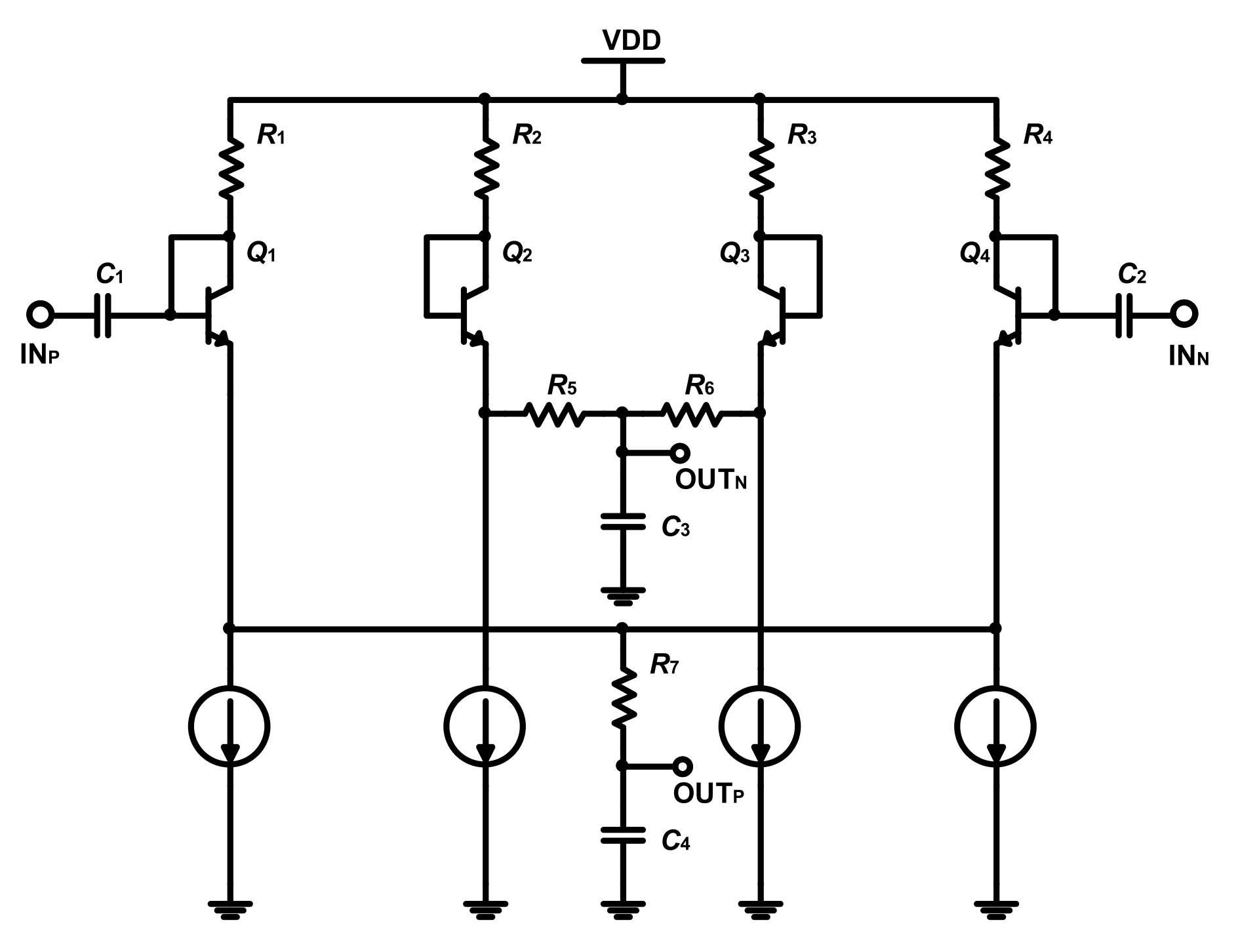
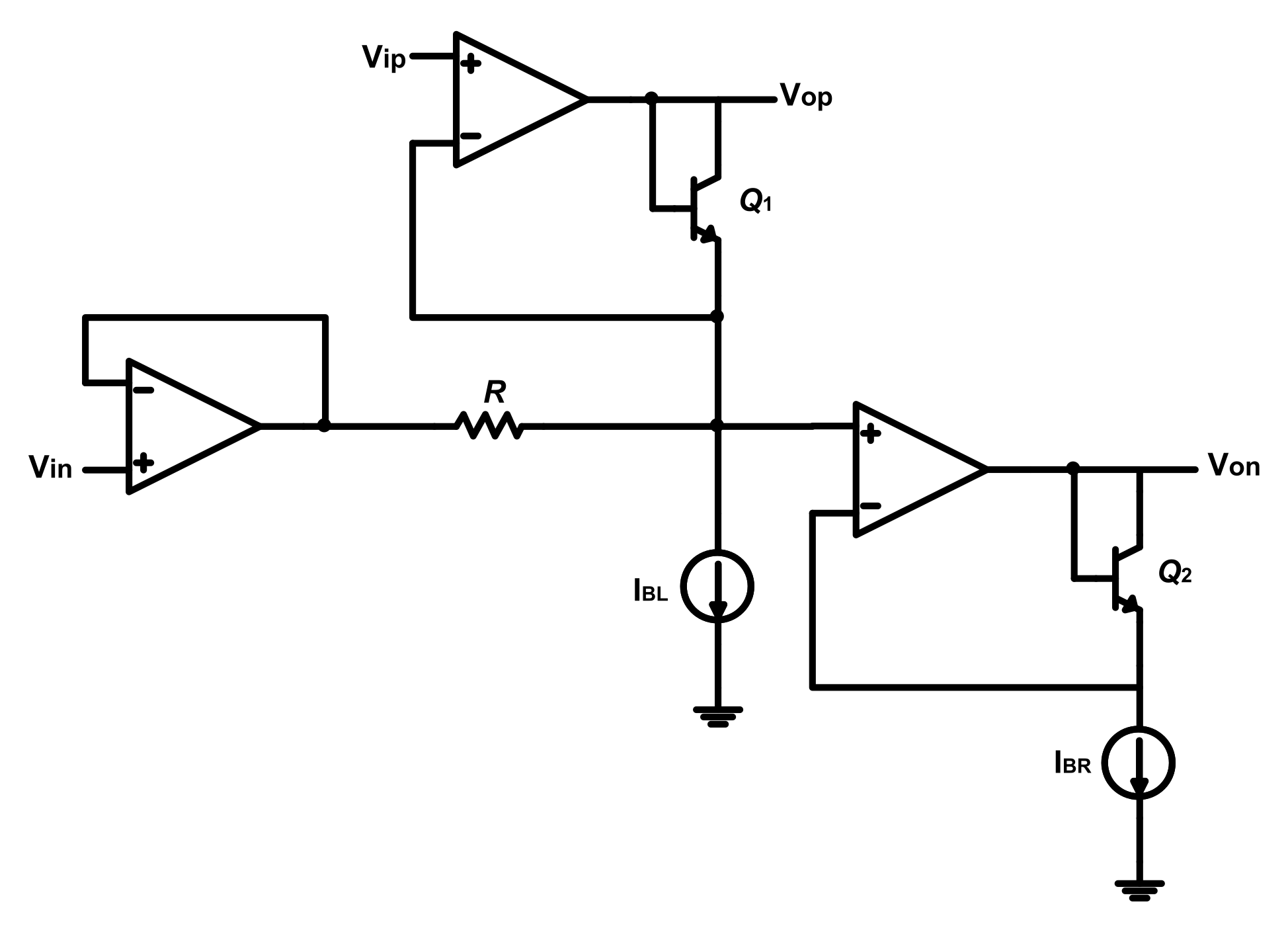
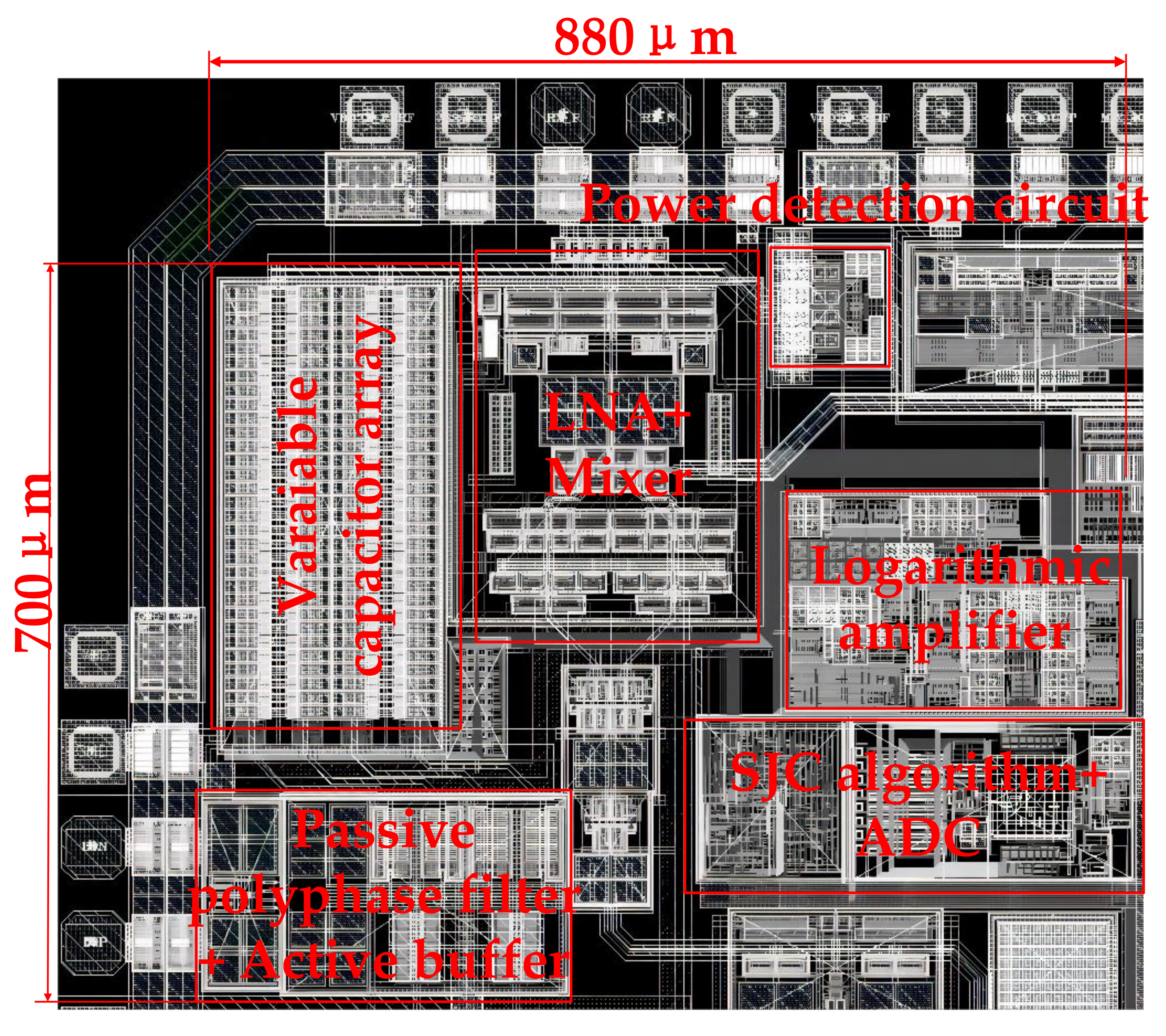
2.1. Overall Architecture of UHF RFID Transceiver and SJC Circuit

Figure 1 shows the UHF RFID transceiver system architecture based on the SJC circuit. The transmitter (TX) and RX are connected to one antenna through a directional coupler. Due to the imperfect isolation of the directional coupler between the TX and RX path, the RX receives a useful signal from the tag and a self-jamming signal from the TX end when the RFID reader works. To deal with this, a sample of the transmitted cancellation signal LO is used to cancel out the self-jammer in the received signal. We adjust the off-chip power amplifier or attenuator in the cancellation signal path to ensure that the power level of the cancellation signal is equal to the largest power level of the self-jamming signal. Then, the phase and amplitude of the cancellation signal are changed through the SJC circuit to make it the same as the leaked carrier amplitude and opposite to the phase. After the signal combiner, most of the self-jamming signals are suppressed. The residual self-jamming signal and useful signal are sent to the low-noise amplifier (LNA) and converted to the baseband through the mixer. Then, the residual self-jamming signal is down-converted into the DC component and can be easily removed by other components.
The sensitivity of the reader is not only limited by the noise of the RX itself but is also influenced by the noise of the cancellation signal and self-jamming signal. According to the range correlation effect, if the time delay between the cancellation signal and the self-jamming signal is small enough, the noise will also be canceled along with the self-jamming signal [16]. So, we take the cancellation signal from another port of the directional coupler and try to keep them on the same path, as shown in Figure 1. The additional noise of the SJC circuit should also be reduced. Therefore, an SJC circuit with a very low noise passive component instead of noisy active devices is adopted in this paper.
The block diagram of the SJC circuit is shown in Figure 2. The cancellation signal LO is converted into a differential signal before the SJC circuit. The differential signal is converted into four signals with the same amplitude and phase of 0°, 90°, 180° and 270° through the passive polyphase filter, respectively. The active buffer compensates for the signal attenuation from the passive polyphase filter and makes the four output impedances consistent. However, if the power of the cancellation signal after the SJC circuit is still larger than the power of the self-jamming signal, the buffer can be removed from this circuit. Then, the variable capacitor array and signal combiner control the amplitude and phase of the cancellation signal, and the output is added to the received self-jamming signal. The feedback network continuously detects the power of the residual signal before the LNA. Due to the high frequency of the self-jamming signal, the residual signal power is converted into linear voltage by a power detection circuit and then sampled by an additional ADC. The power detection circuit also reduces ADC’s design complexity and cancellation algorithm.

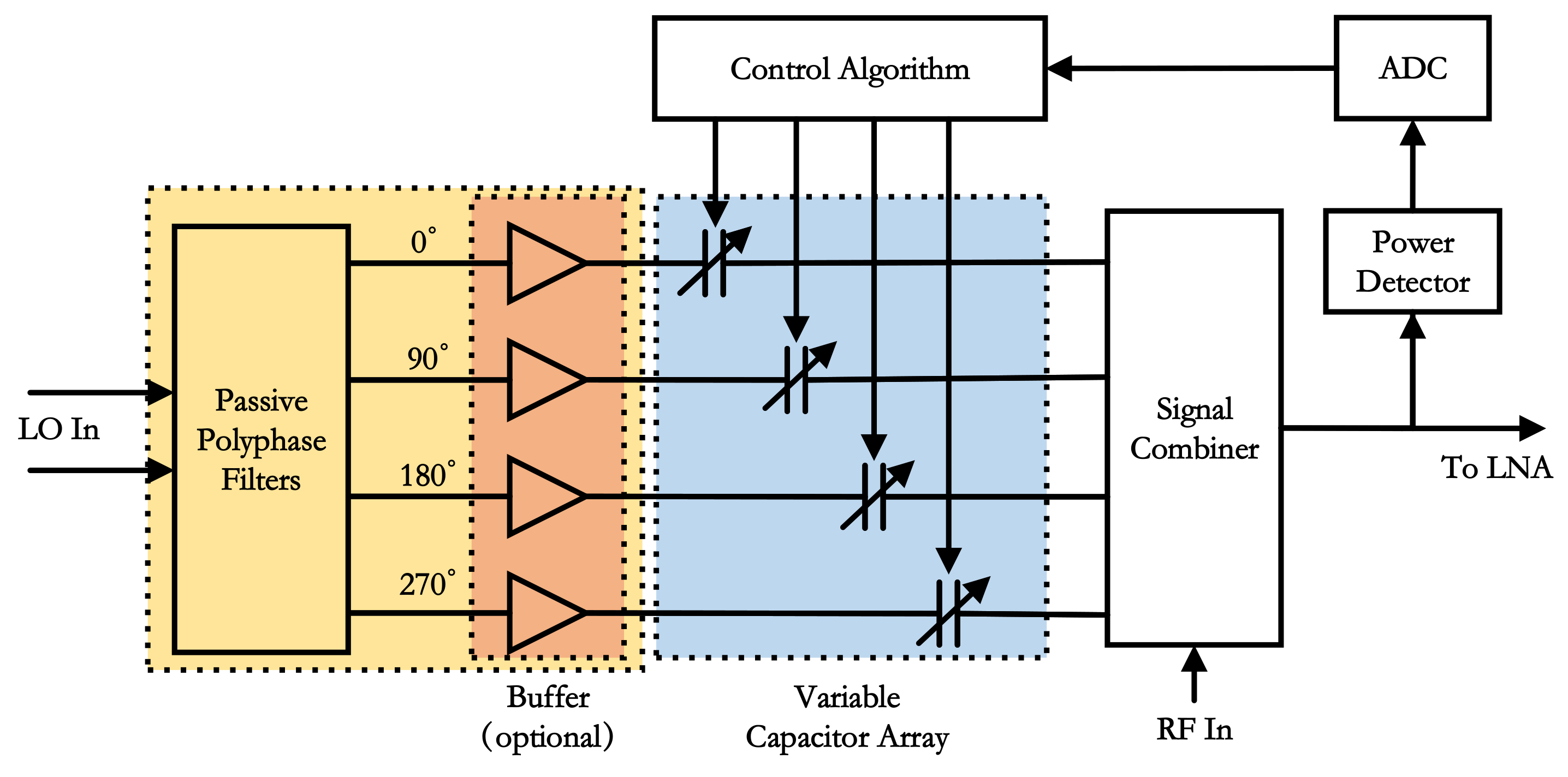
2.2. SJC Circuit Design

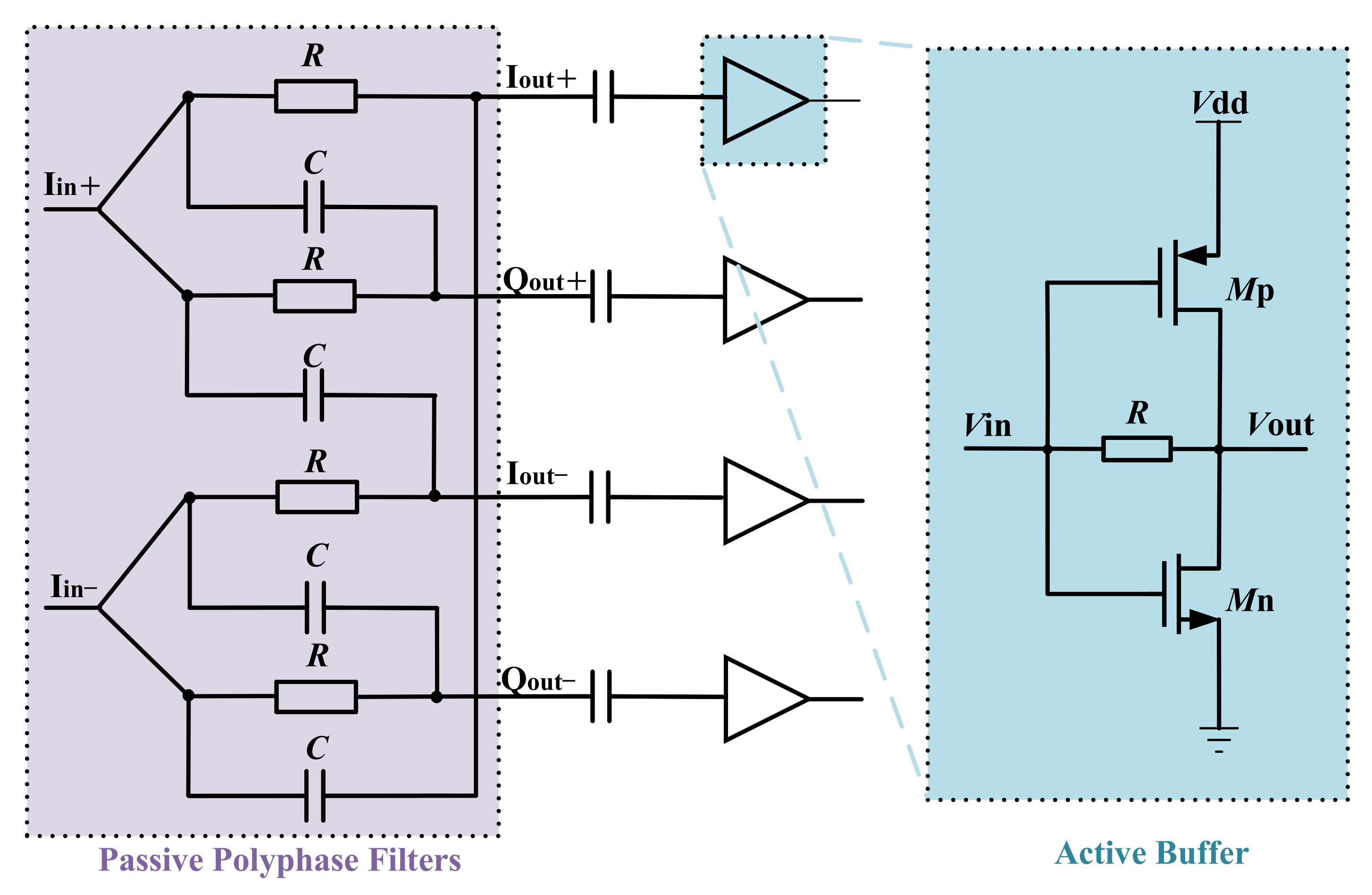
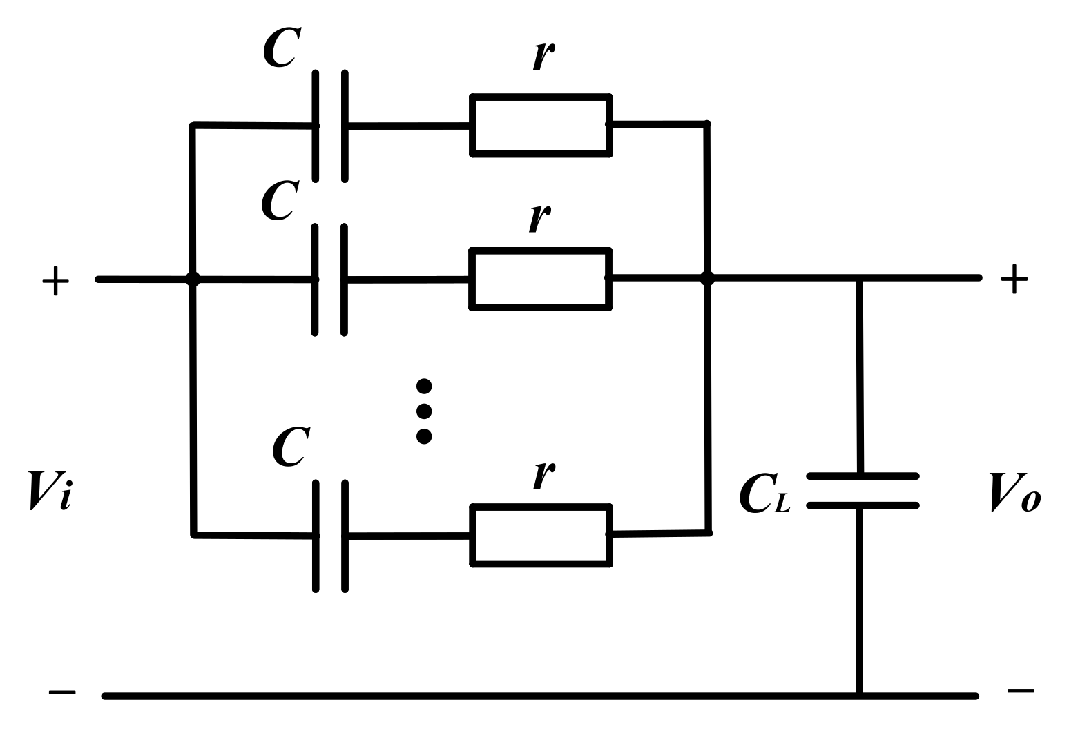
2.2.1. Passive Polyphase Filter

In an RF circuit, the method of generating a quadrature signal includes a coupler [17,18], LC circuit [19], and polyphase filter [20]. The coupler is suitable for narrowband systems, but its size is relatively large, especially for systems below several GHz. The inductance of the LC circuit will also occupy a large area. The polyphase filter adopts resistance and capacitance, which has a small size, relatively wide working frequency, and acceptable insertion loss. Therefore, compared with the other two methods, the polyphase filter has great advantages.
The circuit structure of the passive polyphase filter is shown in Figure 3. The input signals Iin+ and Iin− are differential, and the differential output voltage of channel I and channel Q has the following relationship [21]:
V Iout + V Iout V Qout + V Qout = 1 j ω R C 1 + j ω R C
.
As long as the output impedance is consistent, the output voltage amplitudes of channel I and channel Q are always equal. Only when the working frequency ω = 1 / R C the output phase difference of channel I and channel Q is 90°. Each output is optionally connected with an active buffer to compensate for the signal attenuation caused by the passive polyphase filter. In addition, the single-order polyphase filter works at a single frequency point, so the working bandwidth is narrow. Increasing the order of the polyphase filter can expand the working bandwidth, but it will bring more losses and increase the power consumption and transistor size of the active buffers. Since the working frequency band of UHF RFID is 860–960 MHz, the first-order polyphase filter can meet the requirements after simulation and testing.

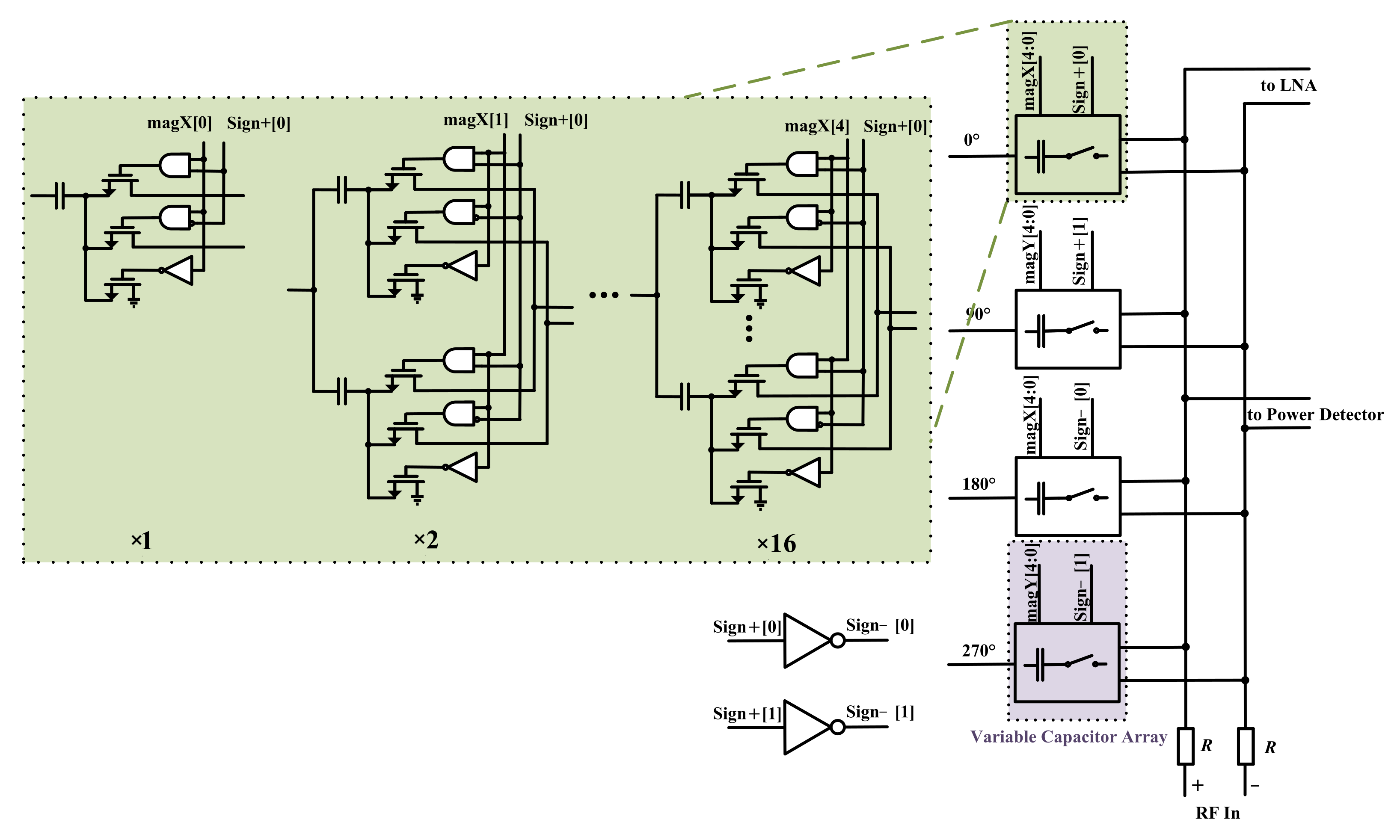
2.2.2. Variable Capacitor Array and Signal Combiner

Figure 4 is a schematic diagram of the unit circuit structure in the variable capacitor array. The main structure includes one capacitor and three switch transistors. The gate of the switch transistor is connected by an AND gate and a NOT gate. The high and low voltage levels are used to turn on and off the switch transistors to carry out amplitude control and polarity control. For example, if both amplitude control MAG and polarity control SIGN are at a high voltage level, M+ is on, M− is off, and the signal is positive. If MAG is at a high level and SIGN is at a low level, M− is on, M+ is off, and the signal is negative. If MAG is at a low level, the polarity control fails, and M+ and M− are turned off at the same time. This capacitor array unit fails. However, this situation will lead to the inconsistency of the overall equivalent impedance of the capacitor array. The addition of Mg can solve this problem. If MAG is high, Mg is off; if MAG is low, Mg is on. Therefore, the capacitor array unit has only one transistor turned on in any case. Connect the output of Mg to the output common mode, and the overall equivalent impedance will be consistent.
A plurality of variable capacitor unit circuits is combined to form a variable capacitor array. The variable capacitor array includes one input, two outputs, one polarity control bit, and several amplitude control bits. Increasing the number of bits of amplitude control can improve the performance of the SJC circuit. However, this will increase the number of variable capacitor units exponentially, resulting in a large circuit area and high-power consumption. If the number of bits of amplitude control is M, 2 M 1 variable capacitor units are required.
One variable capacitor unit can be modeled as a capacitor and a resistor in series. The variable capacitor array consists of 2 M 1 variable capacitor units in parallel.To verify the feasibility of signal attenuation by variable capacitor circuits, the variable capacitor array is equivalent to the circuit model in Figure 5, where C L is equal to the impedance of the output of the variable capacitor array. The number of C represents the number of variable capacitor unit circuits. Assuming that the switch transistors work in the linear region and the equivalent resistance is constant, the transfer function of the circuit is:
H ( j ω ) = 1 j ω C L 1 n 1 j ω C + r + 1 j ω C L = 1 Γ n + 1 .
where Γ = ( 1 + j ω C r ) C L / C is the number of variable capacitor unit circuits. From this formula, it can be seen that the transfer function does not increase linearly with the increase of m. Figure 6 shows the magnitude of H ( j ω ) under different | Γ | values when n < 32. The approximate linearization of the transfer function within a limited n can be achieved by increasing the parameter | Γ |, but this will also lead to severe signal attenuation.
After passing through the polyphase filter, the differential cancellation signals are converted into four signals with the same amplitude and phase of 0°, 90°, 180° and 270°, which are respectively sent to the variable capacitor network after the active buffer. The variable capacitor network consists of four variable capacitor arrays; one variable capacitor array with M = 5 consists of 1 + 2 + 4 + 8 + 16 = 2 M 1 = 31 variable capacitor units. Figure 7 shows the schematic diagram of the variable capacitor network and signal combiner circuit. Two polarity control bits and ten amplitude control bits can be set. The polarity control bits can control the polarity of the two orthogonal signals. The amplitude of each quadrature signal is controlled by 5-bit amplitude control bits. By adding the orthogonal signal vectors with different amplitudes, the cancellation signals with different amplitudes and phases can be obtained. Then, the received signal with a self-jammer is superimposed to complete the cancellation.
Figure 8 shows all possible cancellation points after the cancellation signal passes through the variable capacitor network and signal combiner circuit in an ideal case. The polarity control bits determine the quadrant of the cancellation signal. The amplitude control bits determine the coordinate values of I and Q channels. Assuming that the amplitude attenuation of the variable capacitor unit circuit is linear, the adjacent cancellation points are equidistant. To achieve the result that the self-jamming signal can be effectively canceled under various amplitudes and phases, the square area composed of cancellation points must be able to exactly cover the circular area composed of the maximum power of the self-jamming signal, as shown in Figure 8a. Figure 8b shows that the square area can not cover the power region of the self-jamming signal. So, the cancellation accuracy will be affected if the cancellation signal falls at the boundary in the circular area. The side length of the square area cannot be much larger than the diameter of the circular area. Otherwise, the amplitude control will produce redundant control bits, as shown in Figure 8c.
Within the green region shown in Figure 8, the cancellation accuracy is not equal because of the limited resolution of the cancellation points. Figure 9 shows the distribution of the cancellation points when M = 2, where S j and S c are the given amplitude of the self-jamming signal and the given amplitude of the cancellation signal after vector synthesis, and S r is the residual amplitude of the self-jamming signal, S m is the maximum amplitude of the self-jamming signal. The relationship between them can be expressed as:
S r = S c + S j .
We can conclude that the self-jammer suppression depends on the amplitude of residual self-jamming signal S r . S r = 0 represents that the self-jamming signal sits exactly at the cancellation point. So, the black points are the best cancellation points. On the contrary, the orange point shows the worst self-jammer suppression with S r max = 0.5 S c . We can define the degree of self-jammer suppression η that:
η = 20 log S r S m .
From the analysis shown below, we can draw the theoretical output of η distribution for all possible self-jamming signals in Figure 10. When the residual amplitude of the self-jamming signal S r is small, it has a great suppression, and the color is shown in blue. If the self-jamming signal falls between the cancellation points, it has a bad suppression with the color shown in yellow. We can calculate the maximum η that:
η max = 20 log 2 / 2 2 M 1 .
If M = 2, η max = −12.56 dB, as shown in Figure 10a. With a given S m , if M = 3, the worst case will be η max = −19.91 dB, as shown in Figure 10b. We can see that the overall self-jammer suppression will be improved as M increases. Although η max = −32.84 dB when M = 5, this only occupies a small area. When M is greater than 5, the self-jammer suppression is better theoretically. However, the residual power of the self-jamming signal is weak or completely submerged in noise if we keep increasing M, which means the residual self-jamming signal is below the noise floor. So, increasing M will not always improve the suppression performance.

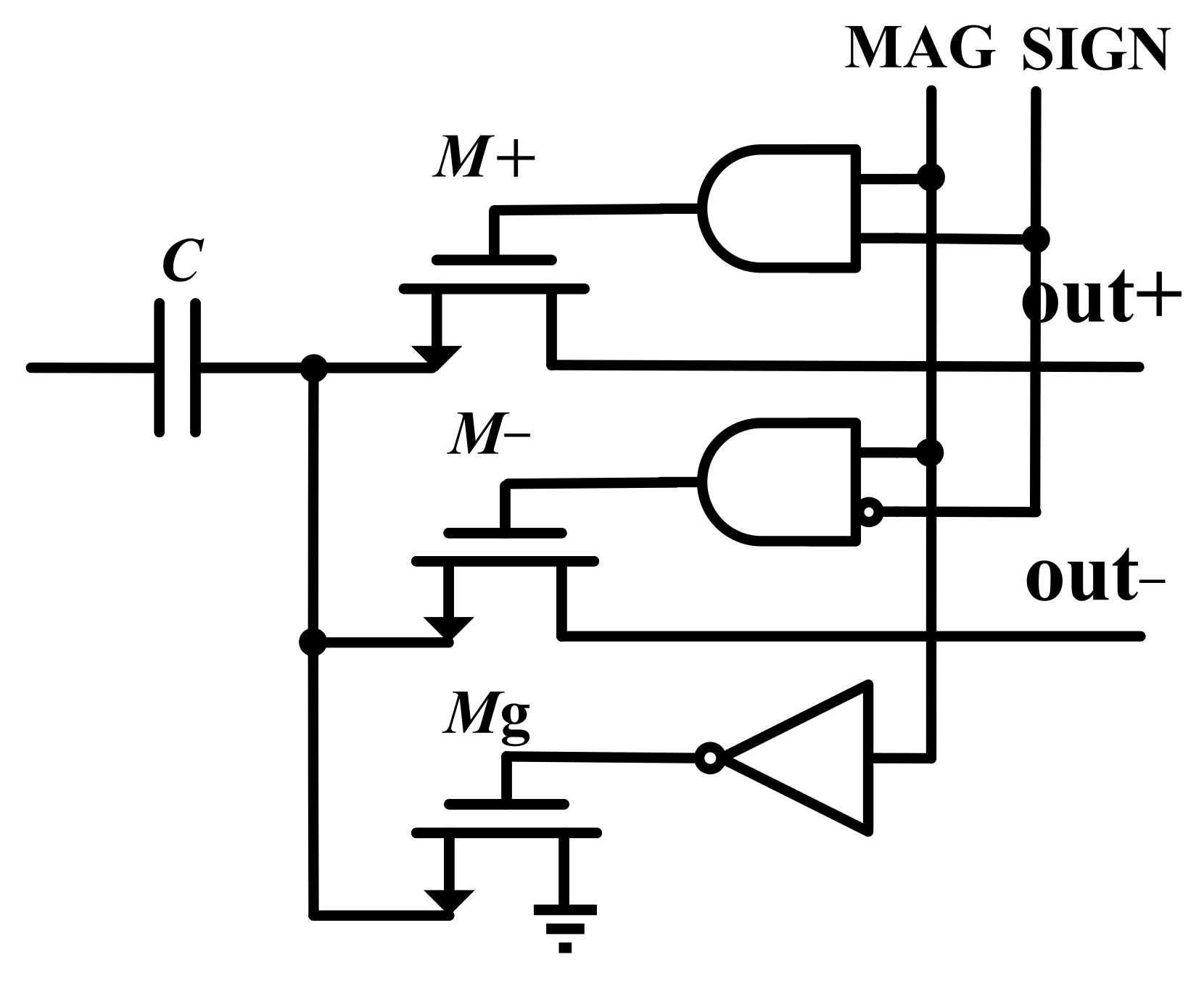
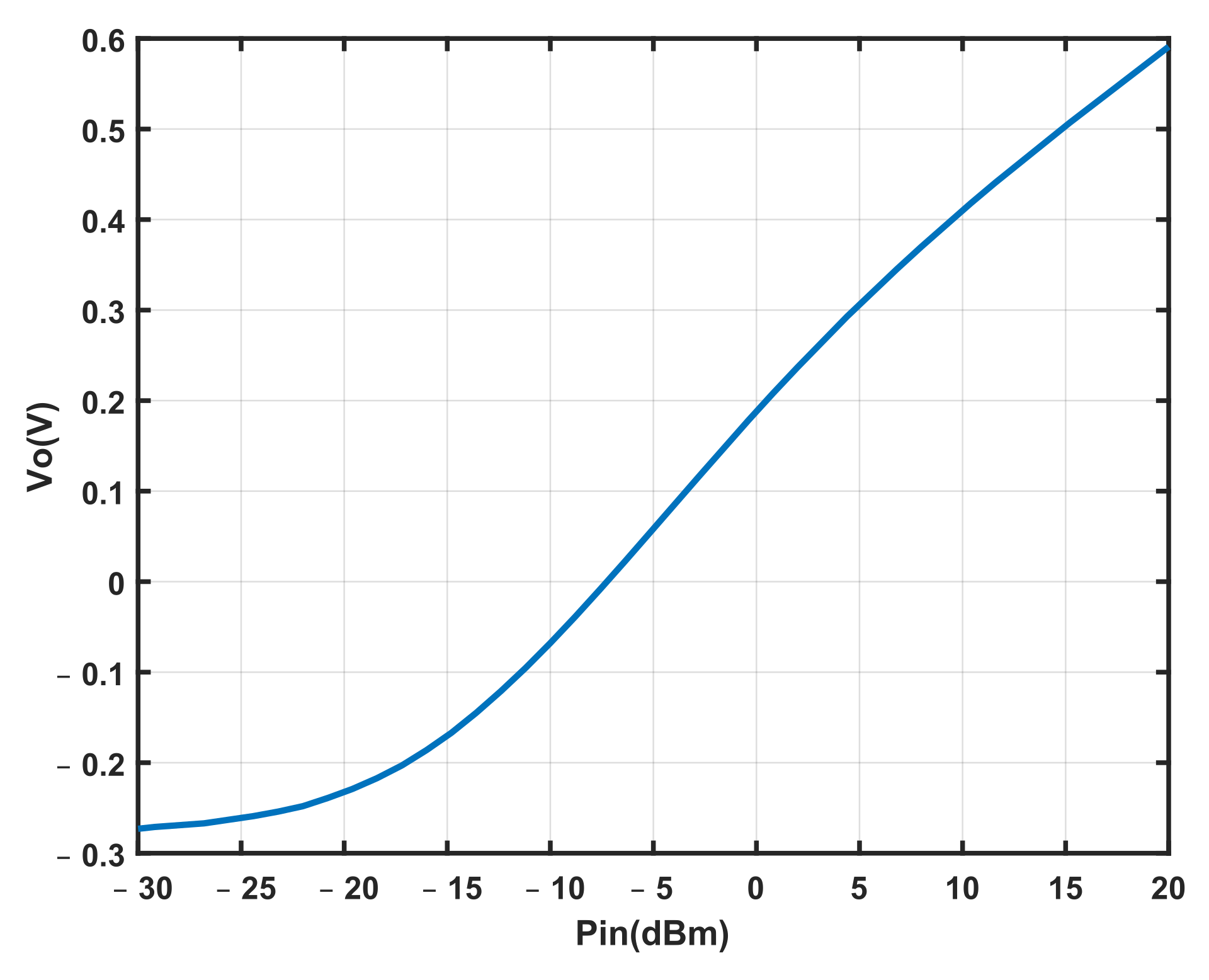
2.2.3. Power Detector

To monitor the residual power after signal cancellation in real time, a power detection circuit is used to convert the residual signal power value to a linear voltage value. Then, ADC is used to convert the linear voltage value to a digital signal and as the input of the self-jammer cancellation algorithm. The power detection circuit consists of a detection circuit and a logarithmic amplifier. The circuit structure of the detection circuit is a bipolar transistor circuit detector proposed in [22], as shown in Figure 11. The transistor Q 1 and Q 4 rectify the residual differential signals after signal cancellation. Q 2 and Q 3 provide the same DC offset as Q 1 and Q 4 , respectively, ensuring that the output DC signal is 0, and the capacitors C 3 and C 4 filter out the AC signal and power noise. The detection circuit has the features of simple structure, wide bandwidth, low power consumption, and good temperature stability.
After converting the power of the residual signal to the DC voltage value, the curve is calibrated by the logarithmic amplifier, and the output voltage varies linearly in dBm with residual signal power. The circuit structure of the logarithmic amplifier is shown in Figure 12. Using the exponential characteristic between the current and the voltage of the bipolar transistor, the following can be obtained:
I BL = V in V ip R + I S e V op V ip V T ,
I BR = I S e V on V ip V T .
where I S is the reverse saturated current V T = k T / q . From (6) and (7):
V op V on = V T ln e 1 I BL I BR e 1 I BR R V in V ip .
It can be seen from (8) that the differential output voltage is logarithmic to the differential input voltage, and there is no reverse saturated current I S in this equation. Therefore, the circuit is less affected by temperature. The zero and slope of the logarithmic amplifier output can be adjusted by changing the I BL and I BR values of the two current sources.
From the input and output results of the power detection circuit in Figure 13, it is shown that the output has a good linear relationship when the input signal power is from −20 to 20 dBm at 900 MHz.

2.2.4. Self-Jammer Cancellation Algorithm

Ideally, a function consisting of all cancellation points only has one extreme point, which is the point that minimizes the residual self-jamming signal power [23]. The cancellation algorithm in this paper uses 5-bit amplitude control bits to control I and Q and 2-bit polarity control bits to control quadrants. After calculating, a total of 3969 possible cancellation points will be obtained, and it is unrealistic to search for all of them. The objective of the cancellation algorithm is to quickly and accurately find the cancellation point that minimizes the residual self-jamming signal power among all possible cancellation points. The commonly used cancellation algorithms can be roughly divided into two categories [23]: local search algorithm and gradient descent search algorithm. The gradient descent algorithm has the least number of searches and the shortest searching time. However, it is easily affected by the noise and interference of the reader. So, the performance is unstable, and the algorithm may not converge. In addition, it is suitable for scenarios with ideal ambient noise and circuit noise [24]. On the other hand, the local search algorithm puts less requirement on the power detector as long as it shows a monotone but not necessarily linear input–output relation [25]. So, the design requirements of the power detector can be appropriately relaxed. In this paper, only local search algorithms are discussed.
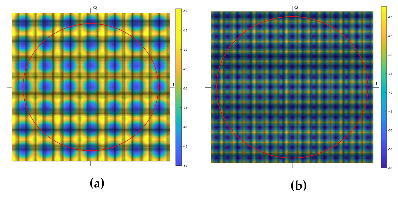
  • Block search algorithm.
The block search algorithm is divided into two steps to reduce the searching time. The coordinate system is established with the differential control signals of I and Q as the horizontal axis and vertical axis. Each point (x, y) in the coordinate system represents that the control signal of I is x and the control signal of Q is y. The algorithm steps are as follows:
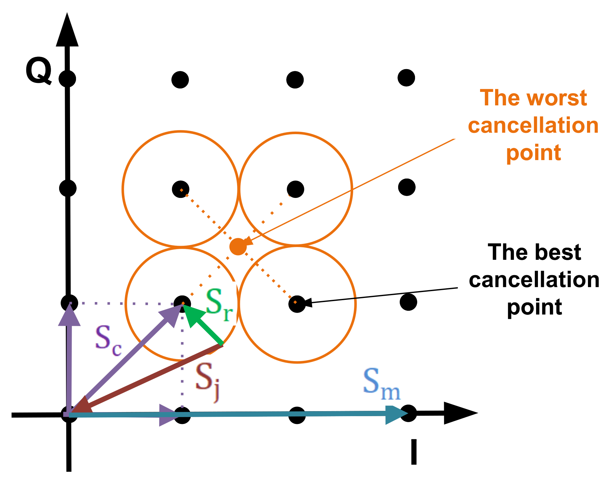
  • Rough search: Divide the whole coordinate system into equal parts according to the m × m lattice. Take any point with the same relative position in each lattice as the input. Find the point that minimizes the residual signal power under this step and record this point as A;
  • Fine search: Search each point in the m × m lattice where point A is located. Find the point that minimizes the residual signal power under this step. Record this point as B. B is the best cancellation point to minimize the residual signal power;
  • After obtaining the best cancellation point, monitor the residual signal power constantly. If the change of residual signal power exceeds the preset value, skip to step 1. Otherwise, it will be monitored all the time.
Since the amplitude control of channel I and channel Q are 5 bits, after adding the polarity control bits, the control range of channel I and channel Q is divided into 2 5 1 + 2 5 1 + 1 = 63 points. So, the total points are 63 2 = 3969 . Assuming that the total number of points is 64 2 = 4096 , it can be obtained that the maximum number of searches required by the block traversal algorithm is m. In order to obtain the minimum number of searches, we have 4096 / m 2 + m 2 2 4096 / m 2 × m 2 = 128 . When taking the equal sign, the value of m is 8. Therefore, when it is divided into an 8 × 8 dot matrix, the search times are at least 128. Since the actual number of points is only 3969, the minimum number of searches may be lower than this value.
  • N-step block search algorithm.
If the whole block search algorithm is divided into N steps, each step divides the lattice searched in the previous step into a new lattice set. Finally, when the size of the lattice reaches the set minimum value, all points of the minimum lattice will be traversed and searched. This traversal algorithm can shorten the total search time.
  • It is assumed that the I-channel and Q-channel signals are divided into 2 6 = 64 points. Divide all points into m equal parts. In order to make the length and width after each bisection an integer, m takes the positive integer power of 2. Take any point with the same relative position in each lattice as the input. Find the point in the lattice where the residual signal power is minimized in this step;
  • Continue to divide the lattice obtained in step 1 into m equal parts. Repeat step 1. The lattice obtained in the previous step is divided into a new lattice set in each step. Finally, when the size of the lattice reaches the set minimum value, all points of the minimum lattice are traversed and searched until the best cancellation point is found;
  • After the best cancellation point is obtained, monitor the residual signal power constantly. If the change of residual signal power exceeds the preset value, skip to step 1. Otherwise, it will be monitored all the time.
Assuming that the algorithm ends when the lattice size is 1 × 1 . The total number of steps of the algorithm is N = log m 2 6 = 6 log m 2 . Each step needs to search m × m points. So, the total number of steps is T = m 2 N = 6 m 2 log m 2 . After derivation calculation, when m = 2 is chosen, the number of steps reaches the minimum, and the total number of steps is 24. This algorithm will significantly reduce the search time because of many discarded points. However, if each step is roughly divided, except near the optimal cancellation point, other sections change slowly with the amplitude of the cancellation signal. If it is roughly divided, the N-step block search algorithm may not find the location of the best cancellation point.
To ensure the stability of the algorithm and shorten the search time, the improved cancellation algorithm used in this paper is shown in Figure 14. The steps are as follows:
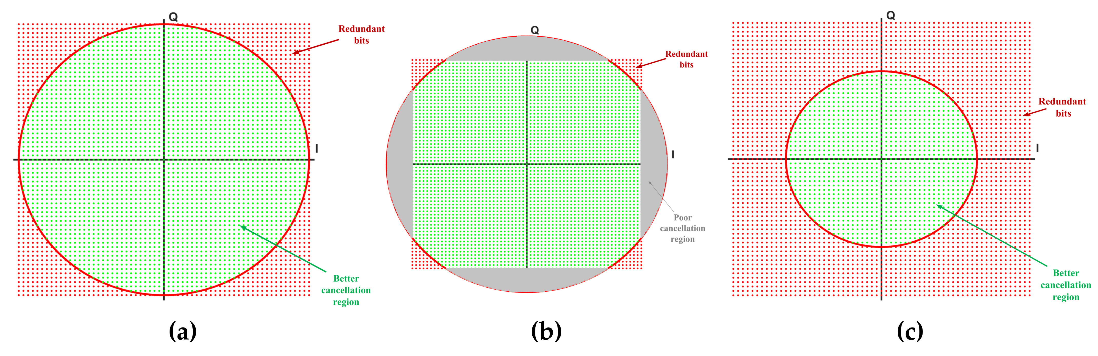
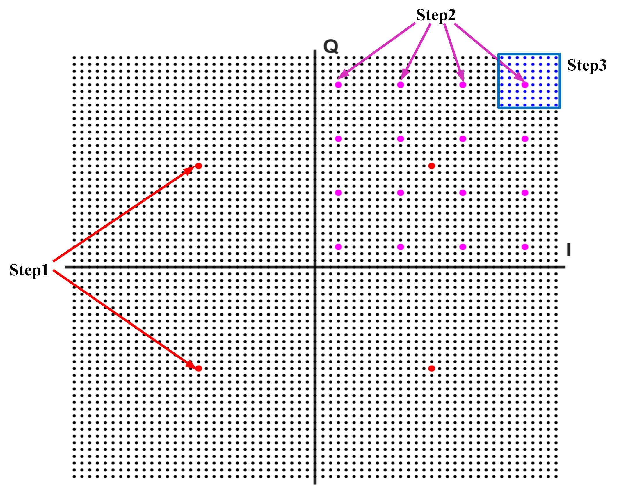
  • Divide all points into four parts according to the four quadrants in the coordinates. Use the coordinates of the central point of each part to control the variable capacitor network, and take the point that minimizes the residual power of the self-jamming signal so as to determine the quadrant;
  • Divide all determined quadrants into an 8 × 8 lattice on average. Take the coordinates of the central point of each lattice into the variable capacitor network. Take the point that minimizes the residual power of the self-jamming signal;
  • Search the last 64 points. The point with the minimum residual power of the self-jamming signal is the best cancellation point.
A total of 4 + 16 + 64 = 84 iterations are required to complete a self-jammer cancellation by this method. At the same time, in order to make the algorithm adapt to the movement of the best cancellation point caused by environmental changes, after finding the best cancellation point, the algorithm must monitor the residual signal power constantly. If it exceeds the preset value, the algorithm will be started again.

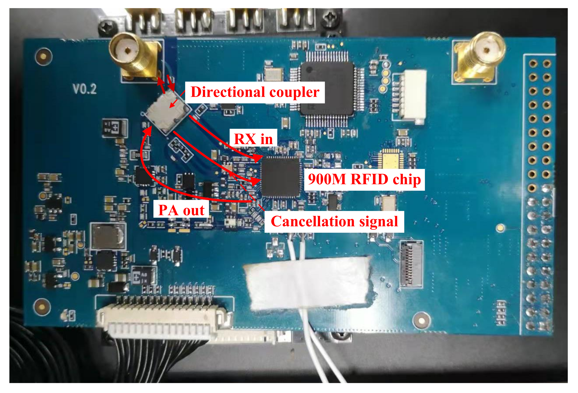
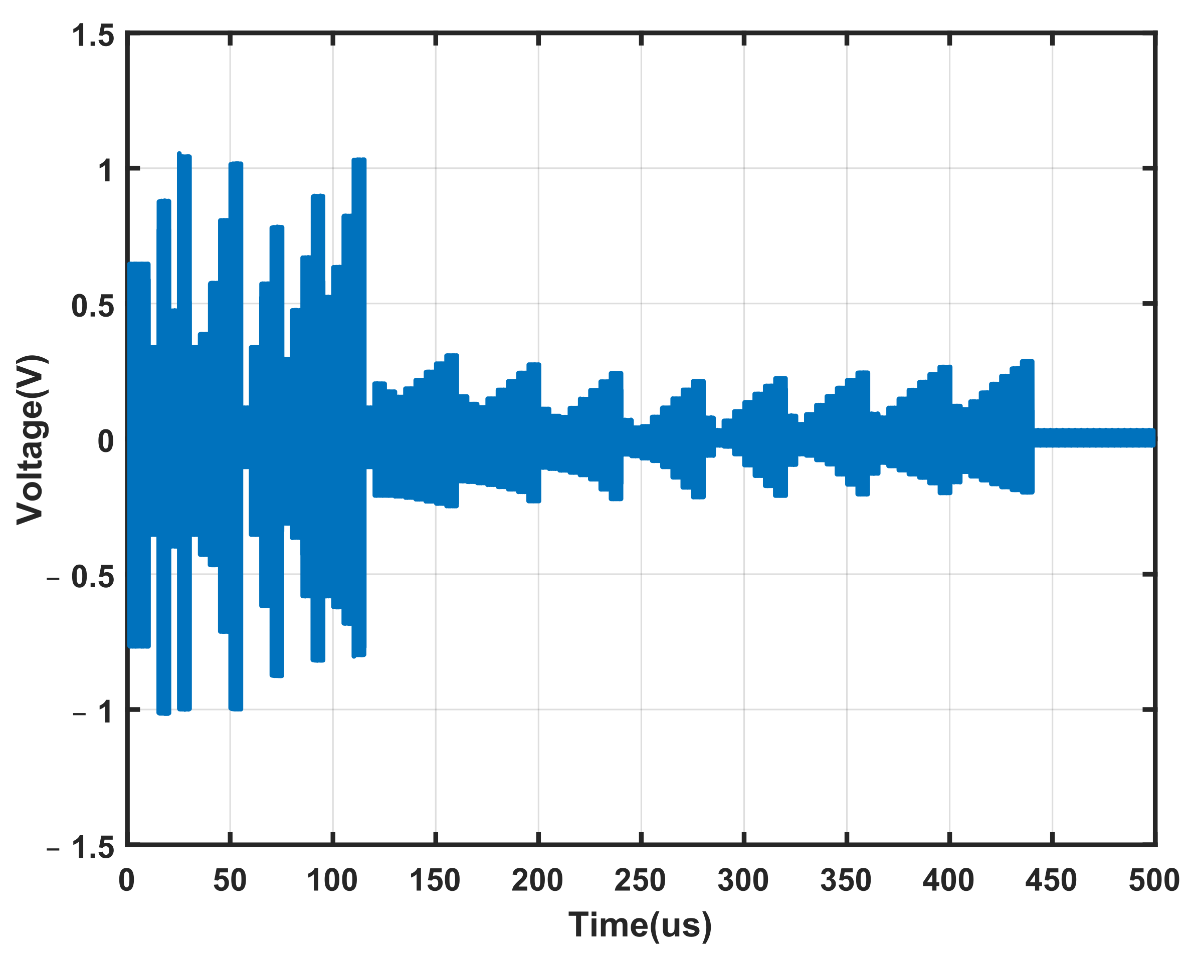
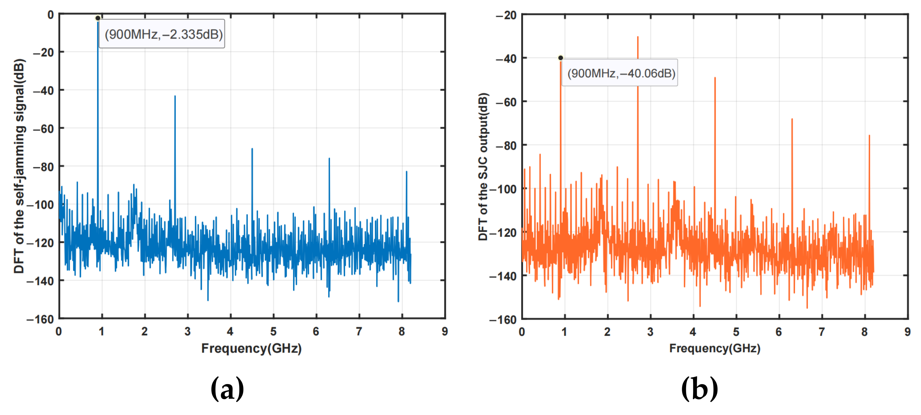
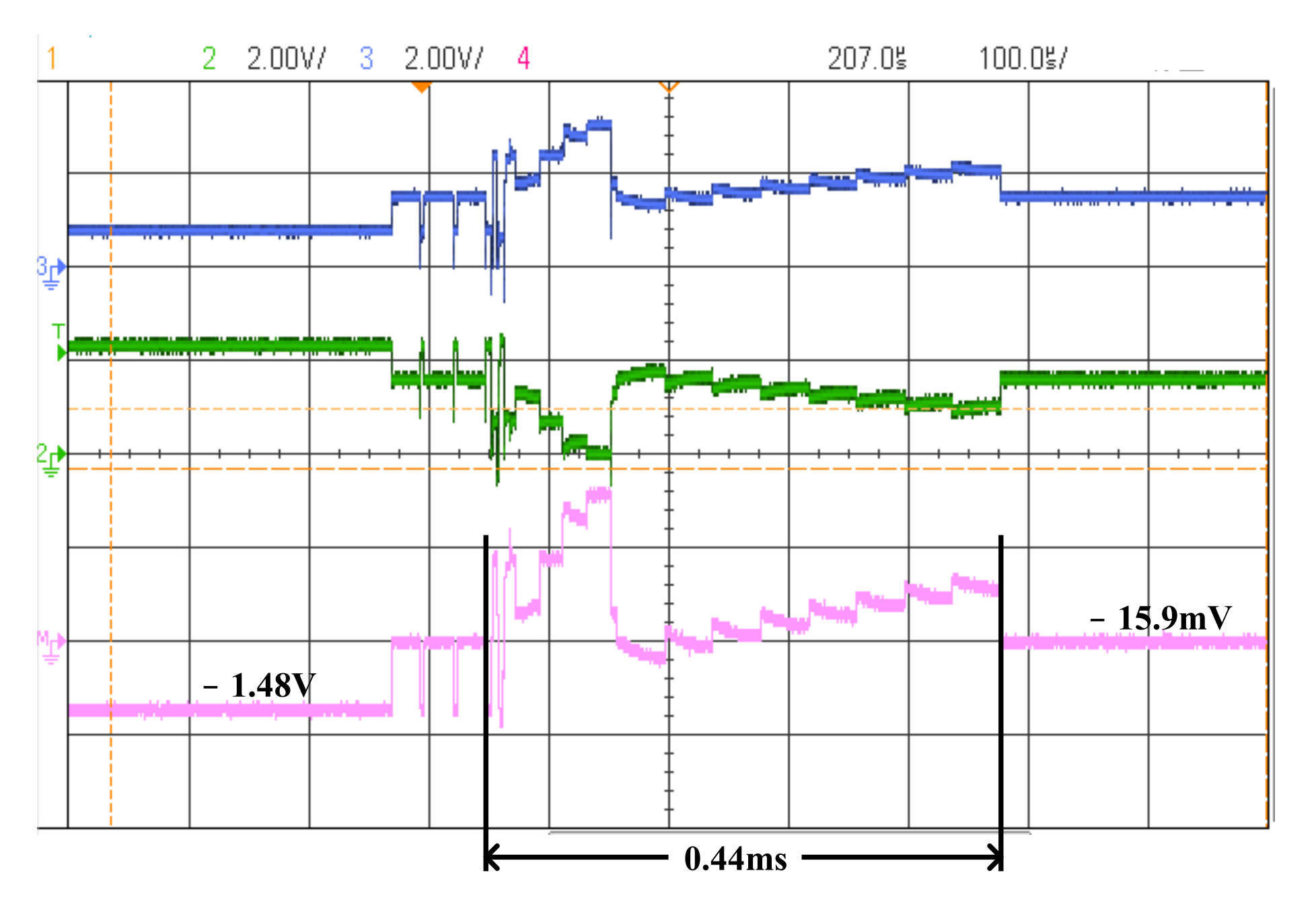
3. Simulation and Experimental Results

The proposed SJC circuit was designed based on the 900 MHz UHF RFID transceiver and was fabricated in a 180 nm CMOS process. The layout photograph of the chip is shown in Figure 15 with a 0.616 mm 2 core area of the SJC circuit. The hardware photo of the 900 MHz RFID test board is shown in Figure 16. The overall function simulation results of the SJC circuit are shown in Figure 17. The simulation results show a residual signal amplitude waveform with time when the working frequency is 900 MHz. Before the SJC circuit works, we need to ensure that the power level of the cancellation signal and the maximum self-jamming signal is the same to achieve a better cancellation effect. From Figure 8a, we can conclude the method to ensure the same power level of these two signals. First, set the output power of the transmitter to maximum; then, turn off the cancellation signal path before the signal combiner. We use the power detector to detect the power level of the self-jamming signal. After that, turn off the self-jamming signal path, and adjust the variable capacitor network so that only the I or Q axis is turned on with no attenuation. So, the power level of the cancellation signal can be detected. If the power level of the two signals is not the same, we adjust the off-chip power amplifier or attenuator in the cancellation path in order to ensure the same power level for a better cancellation effect.
Every time the cancellation algorithm is turned on, it needs to wait for 10 µs to stabilize the ADC and front-end circuit. Then, the cancellation algorithm starts to receive ADC’s output data. Due to the narrow bandwidth of the power detector, the residual signal needs to wait 3 to 4 µs to be sampled by the ADC after passing through the power detector. Therefore, to ensure the stable operation of the cancellation circuit, the cancellation algorithm is set to receive the data output by ADC every 5 µs. As can be seen from Figure 17, after the iteration of the cancellation algorithm, the amplitude of the residual signal gradually decreases. After finding the best cancellation point, the amplitude of the residual signal reaches the minimum. The final convergence time is 440 µs.
Figure 18 shows the spectrum distribution of the self-jamming signal before and after cancellation. It can be seen that the amplitude of the signal at 900 MHz is attenuated by 38 dB after passing through the SJC circuit, and the remaining harmonics will be filtered out by LNA. Figure 19 is a simulation waveform of the time-varying differential output DC level of the mixer. It can be seen that before the cancellation circuit works, the strong co-frequency self-jamming signal generates a high DC voltage at the output of the mixer after down-conversion. After the best cancellation point is found by the cancellation algorithm, the output DC voltage of the mixer is only 21.5 mV. Figure 20 shows the corresponding chip test results. The blue and green waveforms are the single-ended waveform output by the mixer, respectively, and the red is the differential waveform. The simulation and test results show that the self-jamming cancellation circuit designed in this paper can achieve more than a 38 dB cancellation effect, which is enough in our design. Considering a 20 dB isolation of the coupler, the isolation between the output of PA and the input of LNA is 20 dB + 38 dB = 58 dB. The maximum output power of PA in our design is 10 dBm. So, the maximum power of the self-jammer before LNA is 10 dBm − 58 dB = −48 dBm, which leaves enough of a design margin of the P 1 d B of the LNA. A direct conversion structure is adopted in our transceiver to move the residual self-jammer to DC at the output of the mixer. In addition, the DC can be removed by a large AC coupling capacitor, so the baseband circuit will not be affected by the self-jamming signal. Table 1 shows a comparison between this work and state of the art. The settling time of our work can be further improved by increasing the bandwidth of the power detector, since every time input of the cancellation algorithm needs to wait for the power detector to stabilize.
Sensitivity is an important parameter in UHF RFID readers. By applying the SJC circuit before the RF front end, the sensitivity will be improved as long as the gain of the RF front end is not compressed. However, the noise of the system is also an important factor. The phase noise of the CW signal will leak into the receiver together with the self-jammer, and the SJC circuit will also produce noise. To avoid the impact on the sensitivity, the noise in the SJC output should be at least 3 dB smaller than the noise floor. So, the phase noise of the CW signal must be low enough to ensure a sufficient signal-to-noise ratio (SNR) of the CW signal, and the SJC circuit we proposed is an on-chip passive structure that the noise contribution to the output can be neglected.
However, the sensitivity of our UHF RFID chip is only −55 dBm, so we did not compare that parameter in this design. According to the range correlation effect we mentioned earlier [16], if the time delay between the cancellation signal and the self-jamming signal is small enough, the noise will also be canceled along with the self-jamming signal. So, we take the cancellation signal from another port of the directional coupler rather than directly use the LO signal inside the chip. However, we ignored that the mixer of RX should also adopt the CW signal from the SJC input as the LO signal to maintain the high correlation of the phase noise, so the sensitivity is decreased. We will improve this in the next design.
Through the above analysis, we can summarize the methods to improve the sensitivity of the UHF RFID receiver.
  • Add SJC circuit before the RF front end to avoid the gain compression of the amplifier;
  • The noise produced by the SJC circuit and the LO signal must be low enough to ensure a sufficient SNR of the CW signal and the cancellation signal;
  • Lower the time delay between the two inputs of the SJC circuit and the mixer of the receiver to maintain the high correlation of the noise of these signals.

4. Conclusions

In this paper, a passive, low-cost, fully integrated SJC circuit for UHF RFID applications is proposed. To overcome the drawbacks of the active device in the active amplitude and phase control circuits, a passive variable capacitor array and signal combiner is adopted in this design. By analyzing the feasibility of signal attenuation by variable capacitor circuits, we use five control bits to balance the complexity and the performance of the system. The power detector and the improved self-jamming cancellation algorithm are also introduced. Experimental results showed that a suppression of 38 dB can be achieved while consuming 440 us to converge, which is competitive among other works. At last, we discussed the factors affecting the sensitivity of the UHF RFID receiver, and we also gave the methods to improve it.

Author Contributions

Conceptualization, Q.C. and Q.S.; methodology, Q.C., Z.L. and D.J.; software, Q.C., Q.S. and J.X.; validation, Q.C., Q.S. and Z.W.; formal analysis, Q.C.; investigation, Q.C.; resources, Q.C.; writing—original draft preparation, Q.C.; writing—review and editing, Q.C., Y.L. and S.H.; project administration, S.H. and Y.L. All authors have read and agreed to the published version of the manuscript.

Funding

This research was funded by National Key R&D Program of China: 2019YFB2204900.

Institutional Review Board Statement

Not applicable.

Informed Consent Statement

Not applicable.

Data Availability Statement

Not applicable.

Conflicts of Interest

The authors declare no conflict of interest.

References

  1. Finkenzeller, K. RFID Handbook: Radio-Frequency Identification Fundamentals and Applications; Wiley: New York, NY, USA, 2003. [Google Scholar]
  2. Hua, G.; Ma, Y. Study on carrier cancellation in UHF RFID test system. In Proceedings of the 2015 IEEE 6th International Symposium on Microwave, Antenna, Propagation, and EMC Technologies (MAPE), Shanghai, China, 28–30 October 2015; pp. 648–651. [Google Scholar] [CrossRef]
  3. Chiu, S.; Kipnis, I.; Loyer, M.; Rapp, J.; Westberg, D.; Johansson, J.; Johansson, P. A 900 MHz UHF RFID Reader Transceiver IC. IEEE J.-Solid-State Circuits 2007, 42, 2822–2833. [Google Scholar] [CrossRef]
  4. Khannur, P.B.; Chen, X.; Yan, D.L.; Shen, D.; Zhao, B.; Raja, M.K.; Wu, Y.; Sindunata, R.; Yeoh, W.G.; Singh, R. A Universal UHF RFID Reader IC in 0.18-µm CMOS Technology. IEEE J.-Solid-State Circuits 2008, 43, 1146–1155. [Google Scholar] [CrossRef]
  5. Wang, W.; Lou, S.; Chui, K.W.C.; Rong, S.; Lok, C.F.; Zheng, H.; Chan, H.T.; Man, S.W.; Luong, H.C.; Lau, V.K.; et al. A Single-Chip UHF RFID Reader in 0.18 μm CMOS Process. IEEE J.-Solid-State Circuits 2008, 43, 1741–1754. [Google Scholar] [CrossRef]
  6. Guo, Q.; Zhai, Y.; Tan, X.; Min, H. An On-Chip Configurable Receiver With >55-dB Tx Leakage Suppression for UHF RFID Reader. IEEE Microw. Wirel. Compon. Lett. 2019, 29, 357–359. [Google Scholar] [CrossRef]
  7. Kim, S.; Choi, K.S.; Kim, K.M.; Ko, J.; Kim, J.; Lee, S.G. A Low-Noise and Fast-Settling UHF RFID Receiver with Digitally Controlled Leakage Cancellation. IEEE Trans. Circuits Syst. II Express Briefs 2021, 68, 2810–2814. [Google Scholar] [CrossRef]
  8. Koller, M.; Küng, R. Adaptive carrier supression for UHF RFID using digitally tunable capacitors. In Proceedings of the 2013 European Microwave Conference, Nuremberg, Germany, 6–10 October 2013; pp. 943–946. [Google Scholar]
  9. Kim, M.S.; Jung, S.C.; Jeong, J.; Kim, H.; Seo, M.; Ham, J.; Park, C.S.; Yang, Y. Adaptive TX Leakage Canceler for the UHF RFID Reader Front End Using a Direct Leaky Coupling Method. IEEE Trans. Ind. Electron. 2014, 61, 2081–2087. [Google Scholar] [CrossRef]
  10. Ma, Z.; Jiang, Y. Carrier extraction cancellation circuit in RFID reader for improving the Tx-to-Rx isolation. Circuits Devices Syst. IET 2019, 13, 622–629. [Google Scholar]
  11. Mayordomo, I.; Bernhard, J. Implementation of an adaptive leakage cancellation control for passive UHF RFID readers. In Proceedings of the 2011 IEEE International Conference on RFID, Orlando, FL, USA, 12–14 April 2011; pp. 121–127. [Google Scholar] [CrossRef]
  12. You, B.; Bo, Y.; Wen, X.; Qu, L. Implementation of Low-Cost UHF RFID Reader Front-Ends with Carrier Leakage Suppression Circuit. Int. J. Antennas Propag. 2013, 2013, 135203. [Google Scholar] [CrossRef]
  13. Xiong, H.; Shen, C.; Ye, T.T. Broadband and Fast Carrier Cancellation for Backscattered RFID Communications. IEEE Microw. Wirel. Compon. Lett. 2021, 31, 84–87. [Google Scholar] [CrossRef]
  14. Kapucu, K.; Pauli, M.; Dehollain, C. A fast active leakage cancellation method for UHF RFID readers. In Proceedings of the 2017 IEEE International Conference on RFID (RFID), Phoenix, AZ, USA, 9–11 May 2017; pp. 182–186. [Google Scholar] [CrossRef]
  15. Rossi, M.; Liberati, R.M.; Frasca, M.; Richardson, J. Experimental Implementation of a Low-Cost, Fully-Analog Self-Jamming Canceller for UHF RFID Devices. Electronics 2020, 9, 786. [Google Scholar] [CrossRef]
  16. Budge, M.; Burt, M. Range correlation effects on phase and amplitude noise. In Proceedings of the Southeastcon 1993, Charlotte, NC, USA, 4–7 April 1993; pp. 1–5. [Google Scholar] [CrossRef]
  17. Wang, C.W.; Wu, H.S.; Tzuang, C.K.C. CMOS Passive Phase Shifter With Group-Delay Deviation of 6.3 ps at K-Band. IEEE Trans. Microw. Theory Tech. 2011, 59, 1778–1786. [Google Scholar] [CrossRef]
  18. Fang, H.R.; Tang, X.; Mouthaan, K.; Guinvarc’h, R. 180 and 90 Reflection-Type Phase Shifters Using Over-Coupled Lange Couplers. IEEE Trans. Microw. Theory Tech. 2012, 60, 3440–3448. [Google Scholar] [CrossRef]
  19. Lee, H.S.; Min, B.W. W-Band CMOS 4-Bit Phase Shifter for High Power and Phase Compression Points. IEEE Trans. Circuits Syst. II: Express Briefs 2015, 62, 1–5. [Google Scholar] [CrossRef]
  20. Huang, Y.Y.; Jeon, H.; Yoon, Y.; Woo, W.; Lee, C.H.; Kenney, J.S. An Ultra-Compact, Linearly-Controlled Variable Phase Shifter Designed With a Novel RC Poly-Phase Filter. IEEE Trans. Microw. Theory Tech. 2012, 60, 301–310. [Google Scholar] [CrossRef]
  21. Kaukovuori, J.; Stadius, K.; Ryynanen, J.; Halonen, K.A.I. Analysis and Design of Passive Polyphase Filters. IEEE Trans. Circuits Syst. I Regul. Pap. 2008, 55, 3023–3037. [Google Scholar] [CrossRef]
  22. Meyer, R. Low-power monolithic RF peak detector analysis. IEEE J.-Solid-State Circuits 1995, 30, 65–67. [Google Scholar] [CrossRef]
  23. Boaventura, A.; Santos, J.; Oliveira, A.; Carvalho, N.B. Perfect Isolation: Dealing with Self-Jamming in Passive RFID Systems. IEEE Microw. Mag. 2016, 17, 20–39. [Google Scholar] [CrossRef]
  24. Hong, C.M.; Chen, C.M.; Fan, H.K. A New Gradient-Based Search Method: Grey-Gradient Search Method; Springer Inc.: New York, NY, USA, 1999. [Google Scholar]
  25. Lasser, G.; Langwieser, R. Automatic leaking carrier canceller adjustment techniques. EURASIP J. Embed. Syst. 2013, 2013, 8. [Google Scholar] [CrossRef] [Green Version]
  26. Jung, J.Y.; Park, C.W.; Yeom, K.W. A Novel Carrier Leakage Suppression Front-End for UHF RFID Reader. IEEE Trans. Microw. Theory Tech. 2012, 60, 1468–1477. [Google Scholar] [CrossRef]
  27. Ghahremani, A.; Rezaei, V.D.; Sharif Bakhtiar, M. A UHF-RFID Transceiver with a Blocker-Canceller Feedback and +30 dBm Output Power. IEEE Trans. Circuits Syst. I Regul. Pap. 2013, 60, 3043–3054. [Google Scholar] [CrossRef]
Figure 1. The architecture of the UHF RFID transceiver.
Electronics 11 02311 g001
Figure 2. The architecture of the SJC circuit.
Electronics 11 02311 g002
Figure 3. Schematic diagram of passive polyphase filter and active buffer.
Electronics 11 02311 g003
Figure 4. The unit circuit structure of the variable capacitor array.
Electronics 11 02311 g004
Figure 5. Equivalent circuit model of the variable capacitor array.
Electronics 11 02311 g005
Figure 6. The transfer function of variable capacitor array.
Electronics 11 02311 g006
Figure 7. Variable capacitor network and signal combiner circuit.
Electronics 11 02311 g007
Figure 8. Possible cancellation points and power region of the self-jamming signal. (a) The self-jamming signal can be canceled in all cases; (b) the cancellation accuracy will be affected at the boundary in the circular area; (c) the amplitude control will produce redundant control bits.
Electronics 11 02311 g008
Figure 9. Distribution of the cancellation points when M = 2.
Electronics 11 02311 g009
Figure 10. The output of η distribution when (a) M = 2 and (b) M = 3.
Electronics 11 02311 g010
Figure 11. Schematic diagram of the detection circuit.
Electronics 11 02311 g011
Figure 12. Schematic diagram of the logarithmic amplifier.
Electronics 11 02311 g012
Figure 13. The input–output characteristics of the power detection circuit.
Electronics 11 02311 g013
Figure 14. Schematic diagram of self-jamming cancellation algorithm.
Electronics 11 02311 g014
Figure 15. Layout photograph of the SJC circuit.
Electronics 11 02311 g015
Figure 16. Hardware photo of the 900 MHz RFID test board.
Electronics 11 02311 g016
Figure 17. Simulation result of the differential output of the SJC circuit.
Electronics 11 02311 g017
Figure 18. Suppression performance of the proposed SJC circuit: (a) amplitude of the self-jamming signal; (b) amplitude of the SJC output.
Electronics 11 02311 g018
Figure 19. Simulation result of the differential output of the mixer.
Electronics 11 02311 g019
Figure 20. The chip test result of the differential output of the mixer.
Electronics 11 02311 g020
Table 1. Comparison between this work and state of the art.
MWCL 2021 [13]RFID 2017 [14]TMTT 2012 [26]TCAS-I 2013 [27]MWCL 2019 [6]TCAS-II 2021 [7]This Work
TechnologyN/AN/AN/A0.18 µm CMOS0.13 µm CMOS55 nm CMOS0.18 µm CMOS
Integration (-chip)offoffoffonononon
Self-jamming Suppression (dB)46.2–61.750363514.743.838
Settling Time (ms)0.5200.40.0330.0090.0270.44
Publisher’s Note: MDPI stays neutral with regard to jurisdictional claims in published maps and institutional affiliations.

