
Evaluation of GaN HEMTs in H3TRB Reliability Testing


Abstract
:1. Introduction
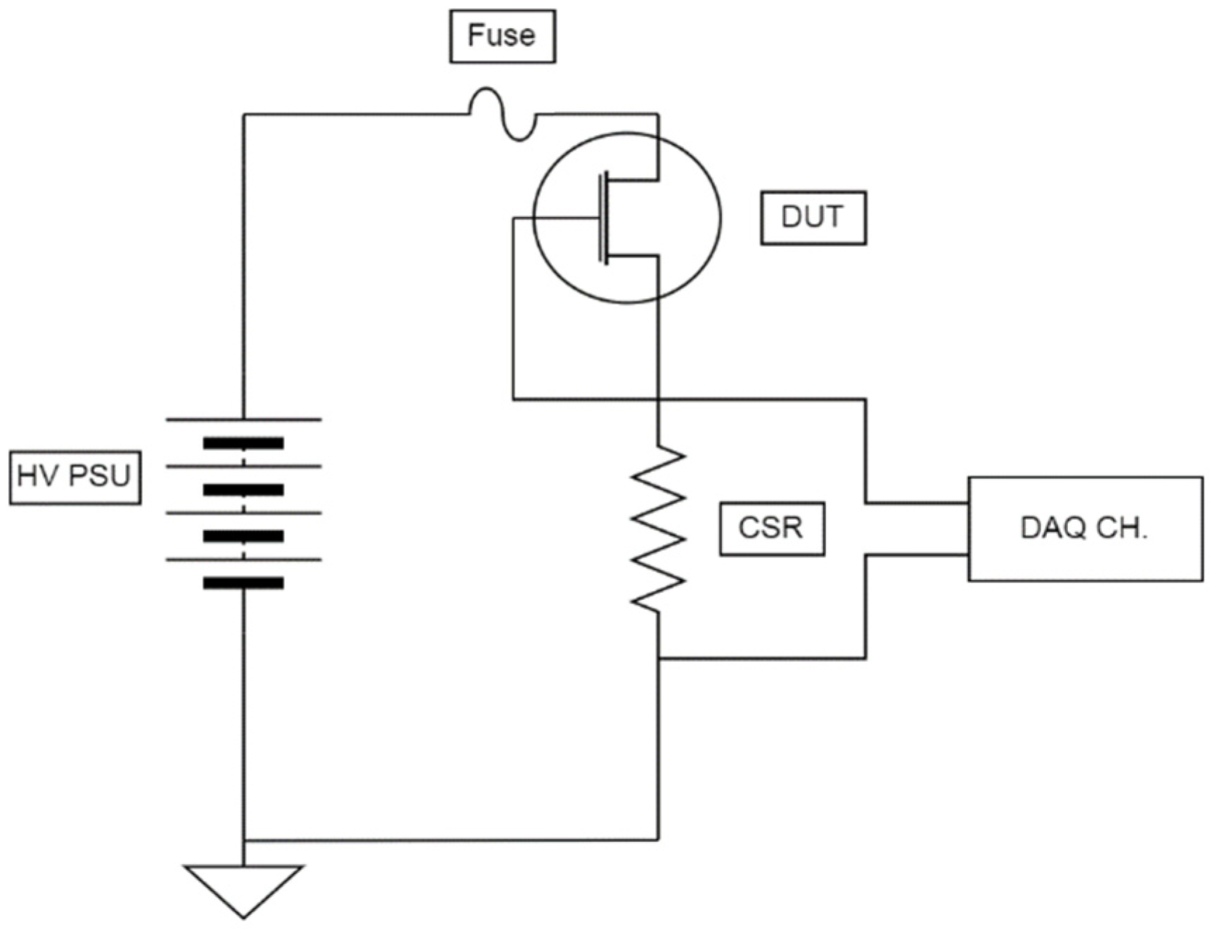
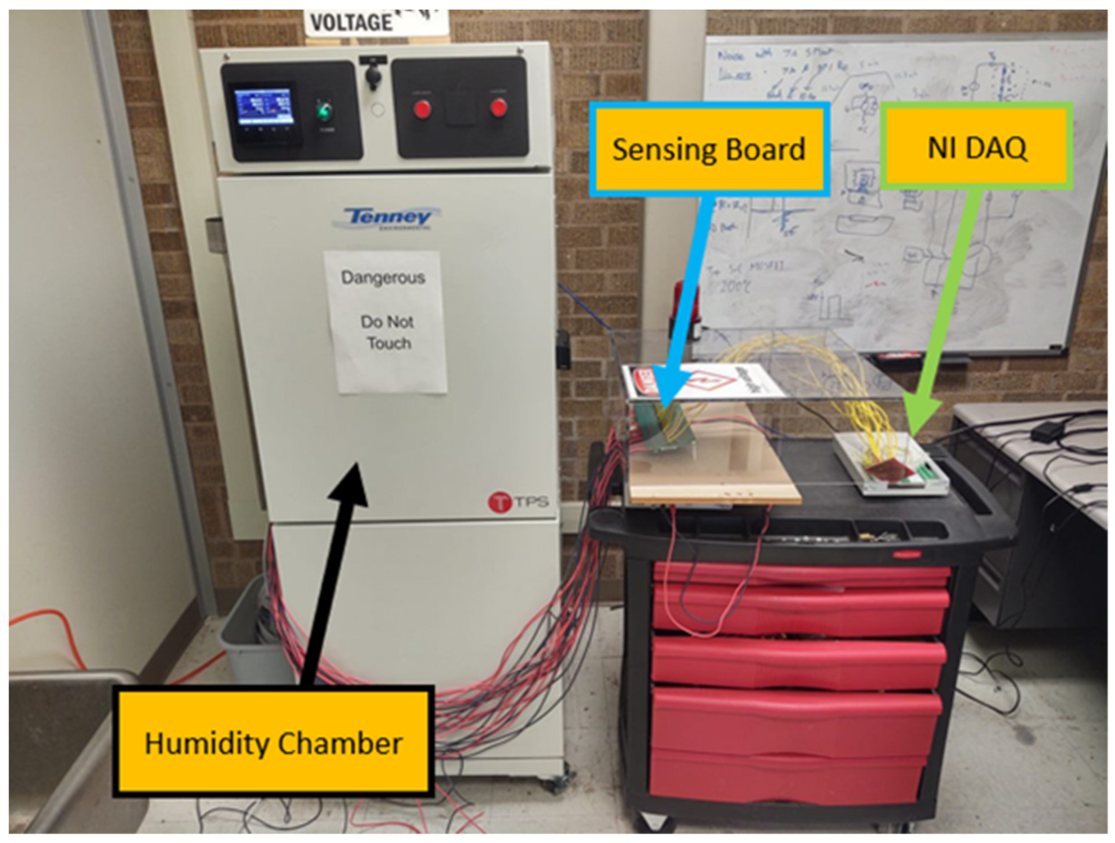
2. Methodology
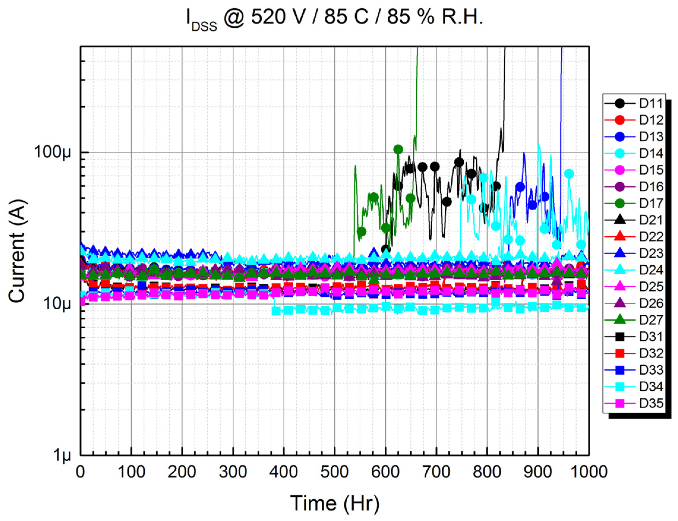
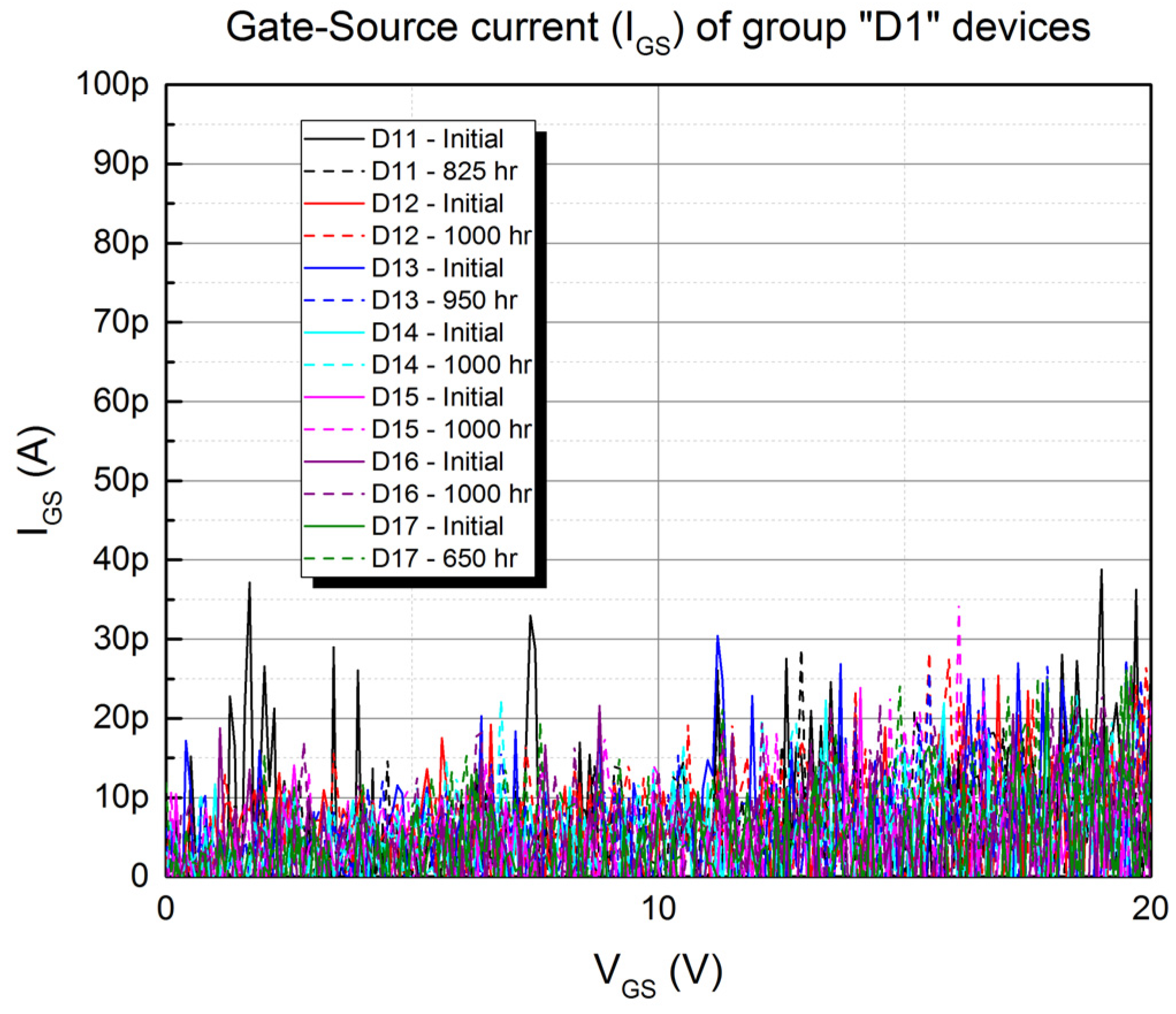
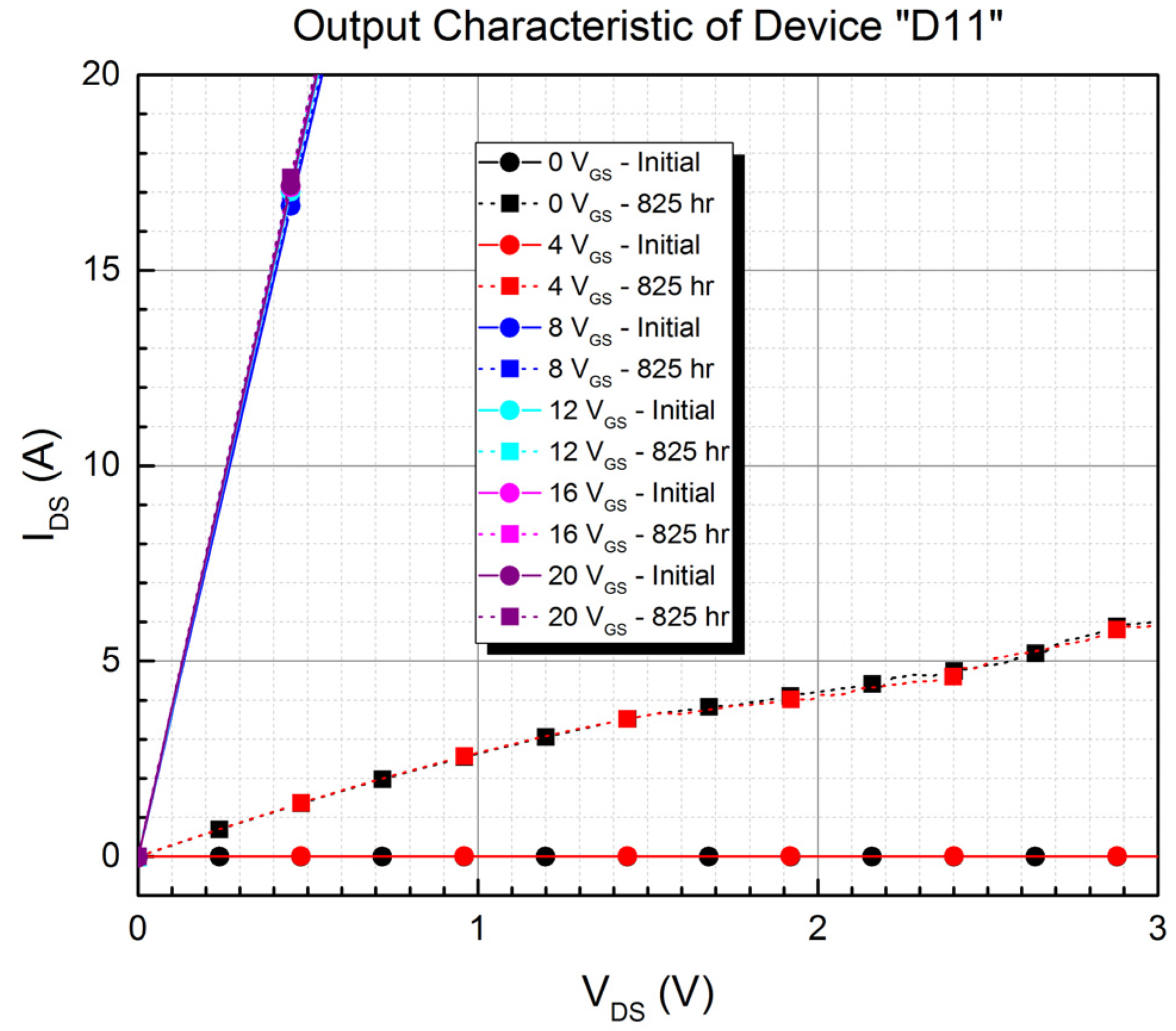
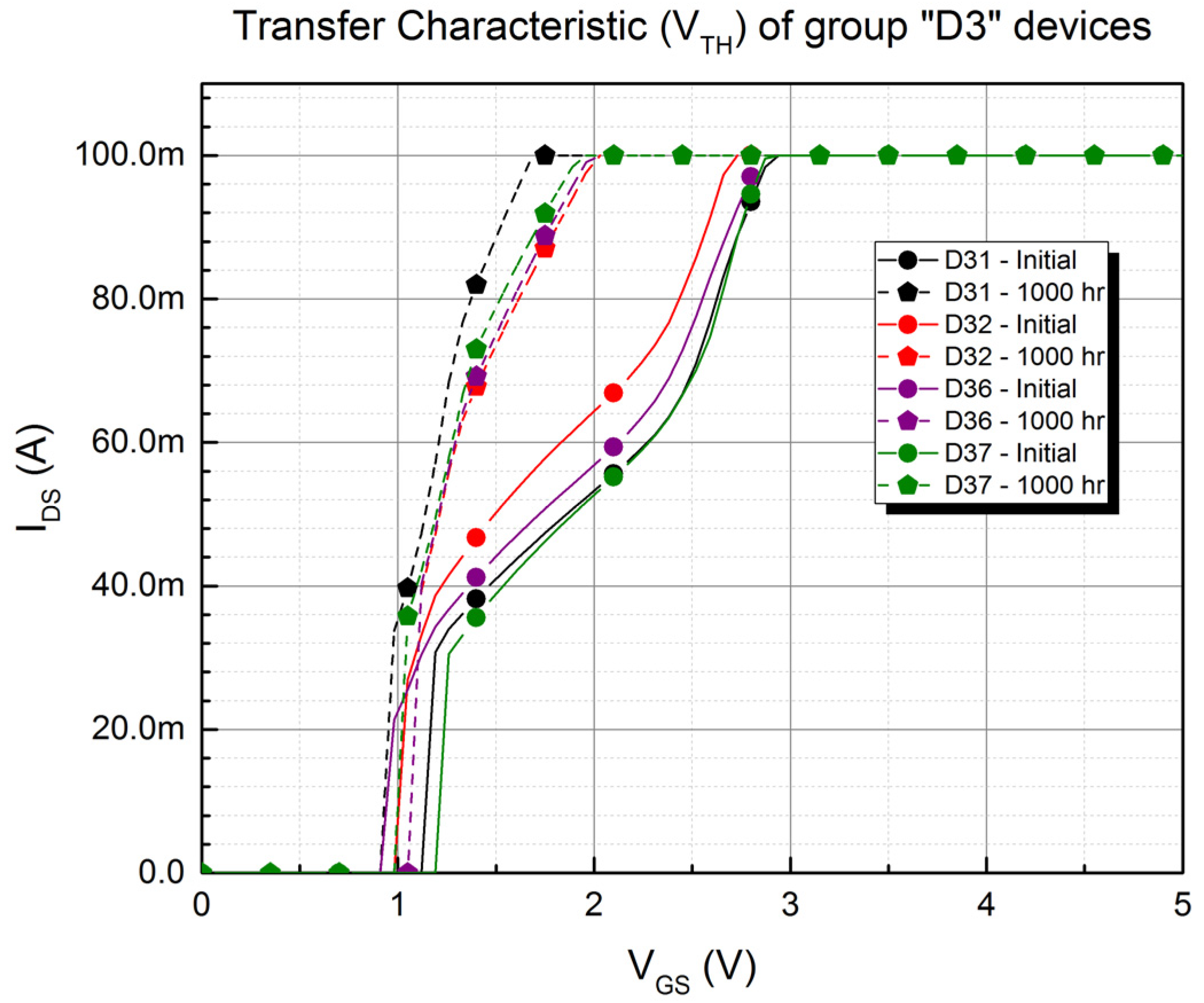
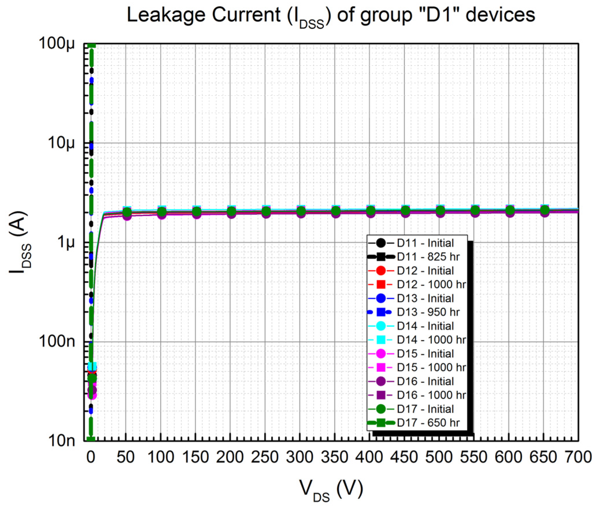
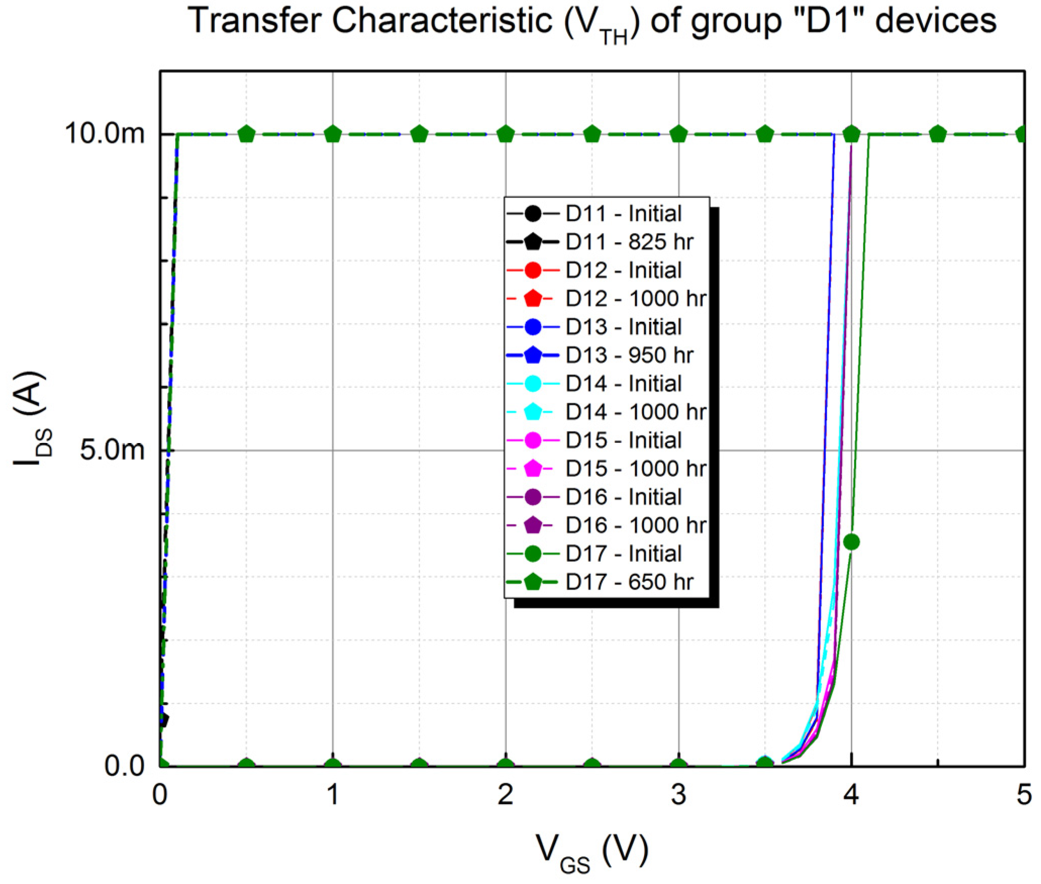
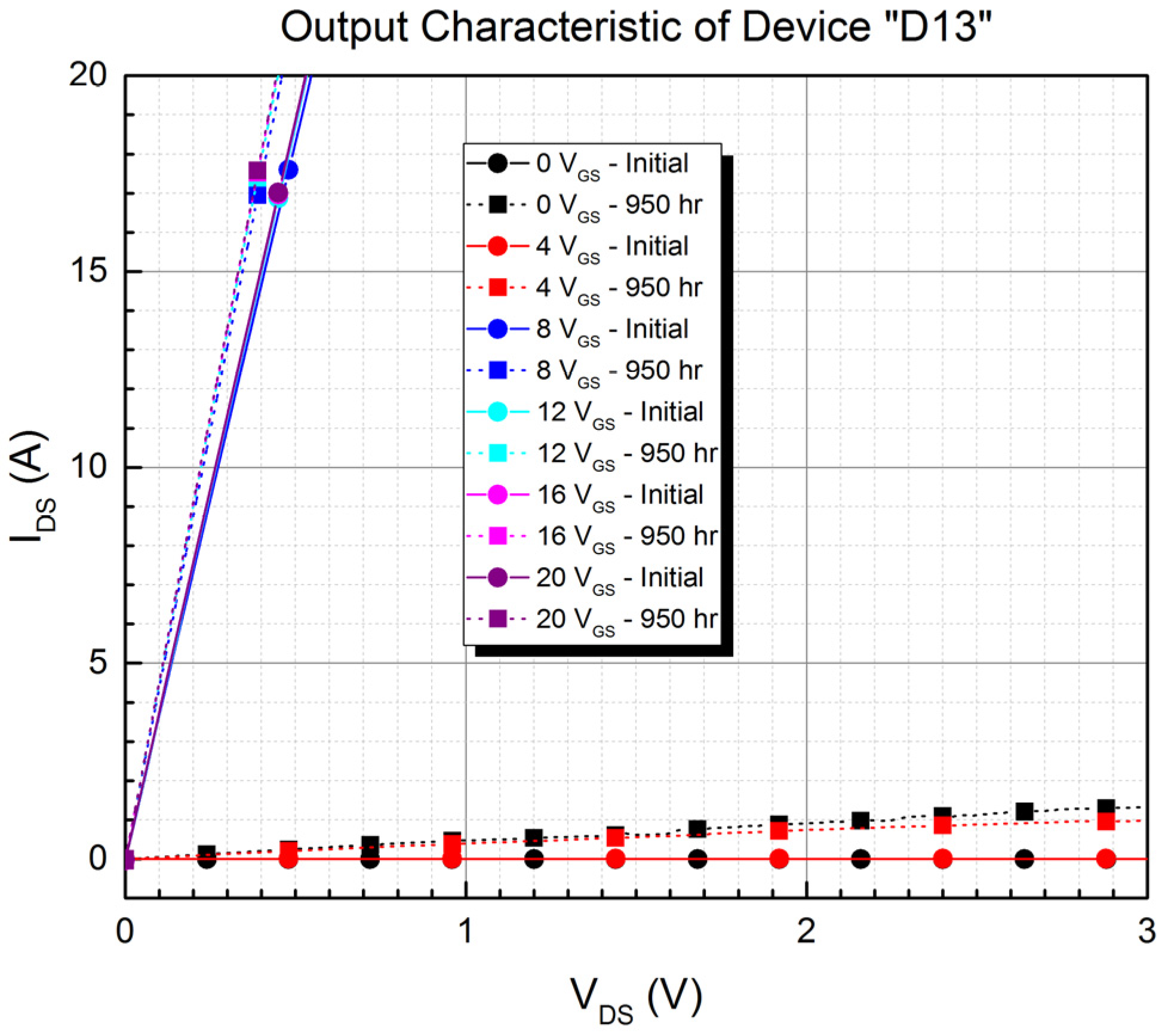
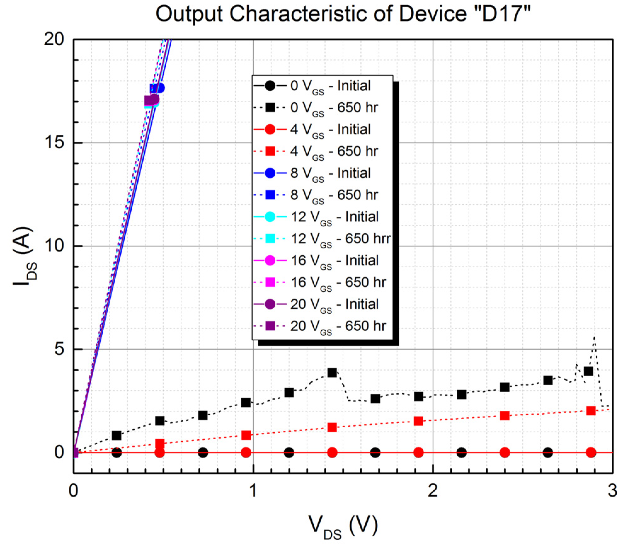
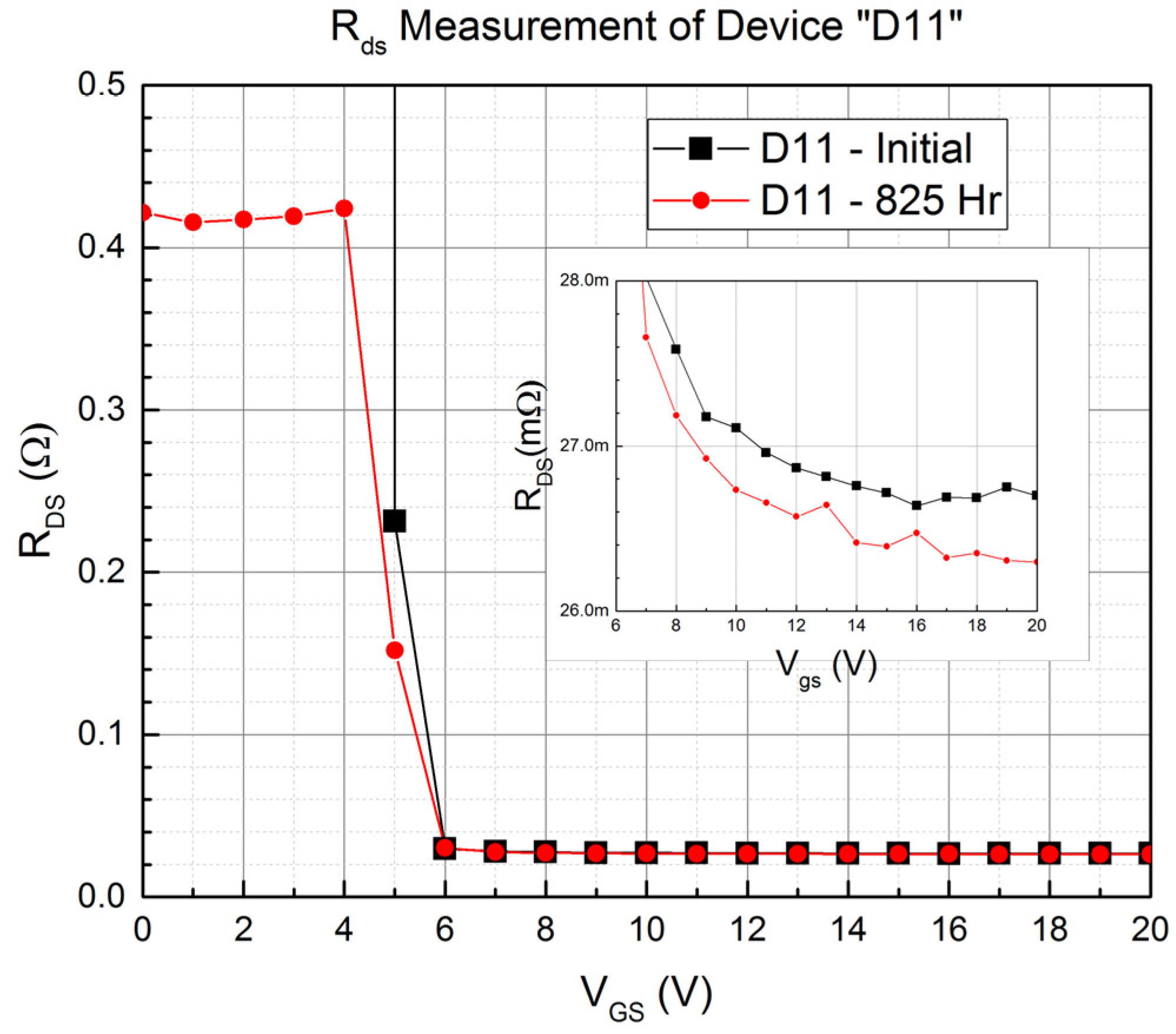
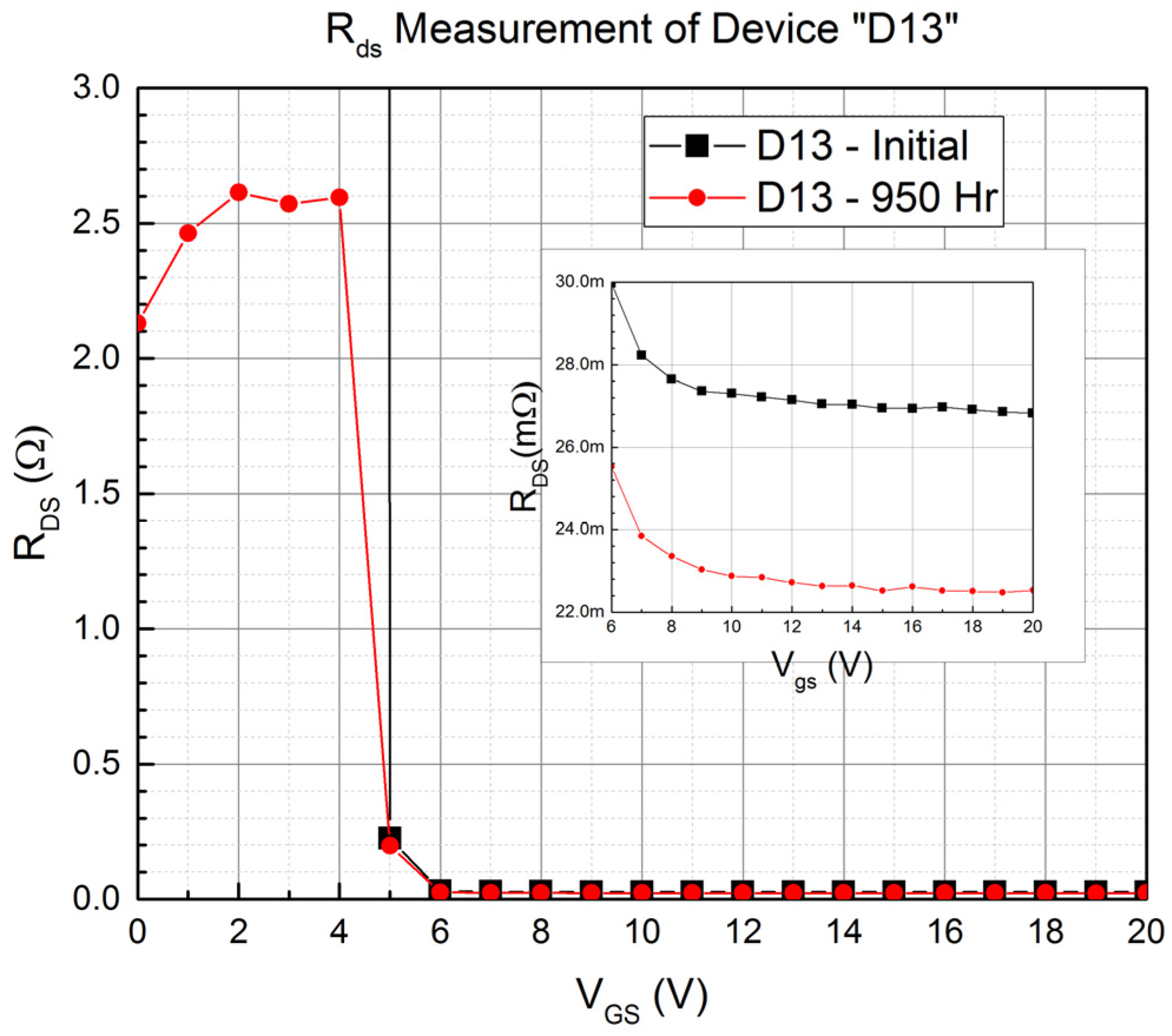
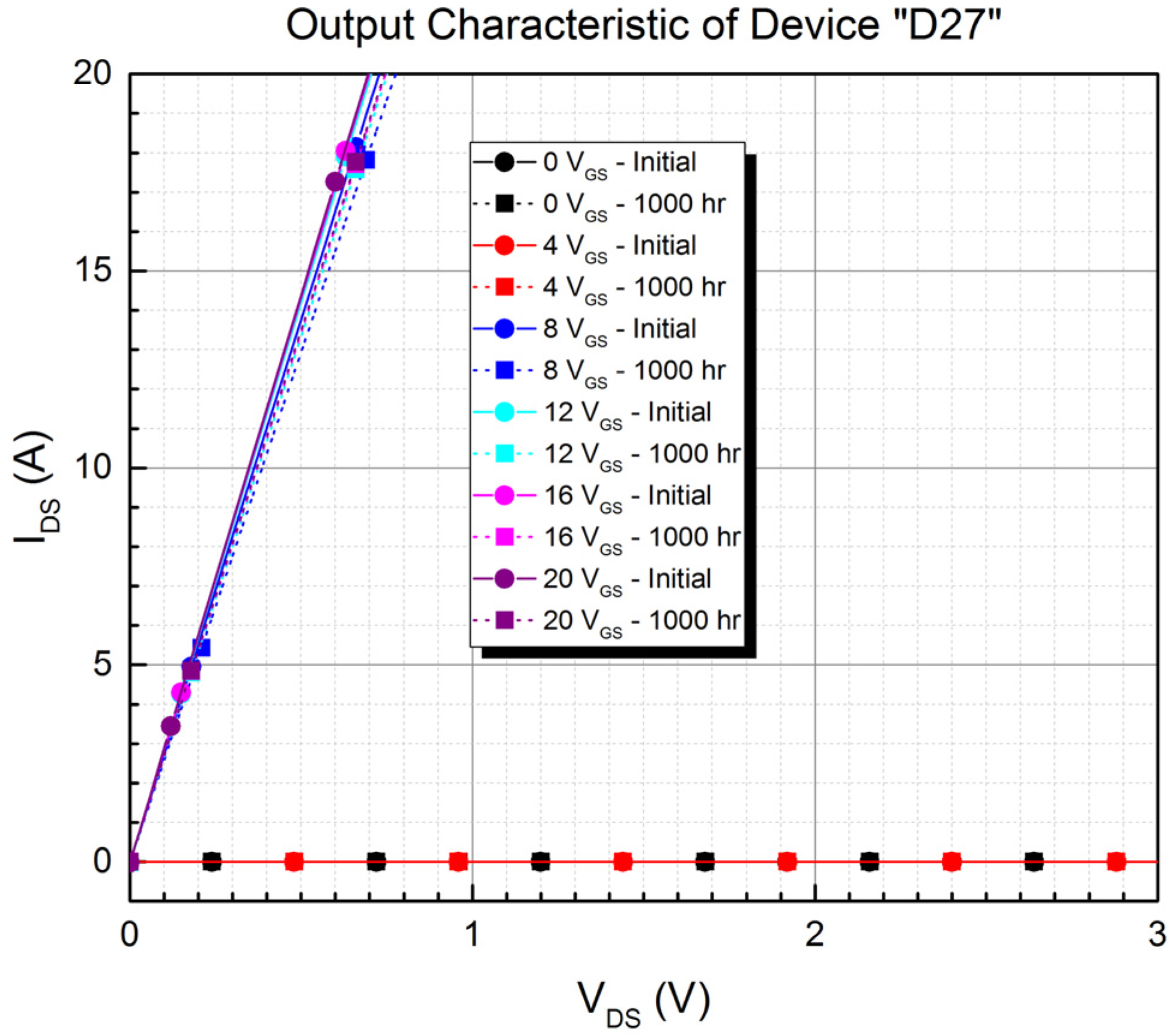
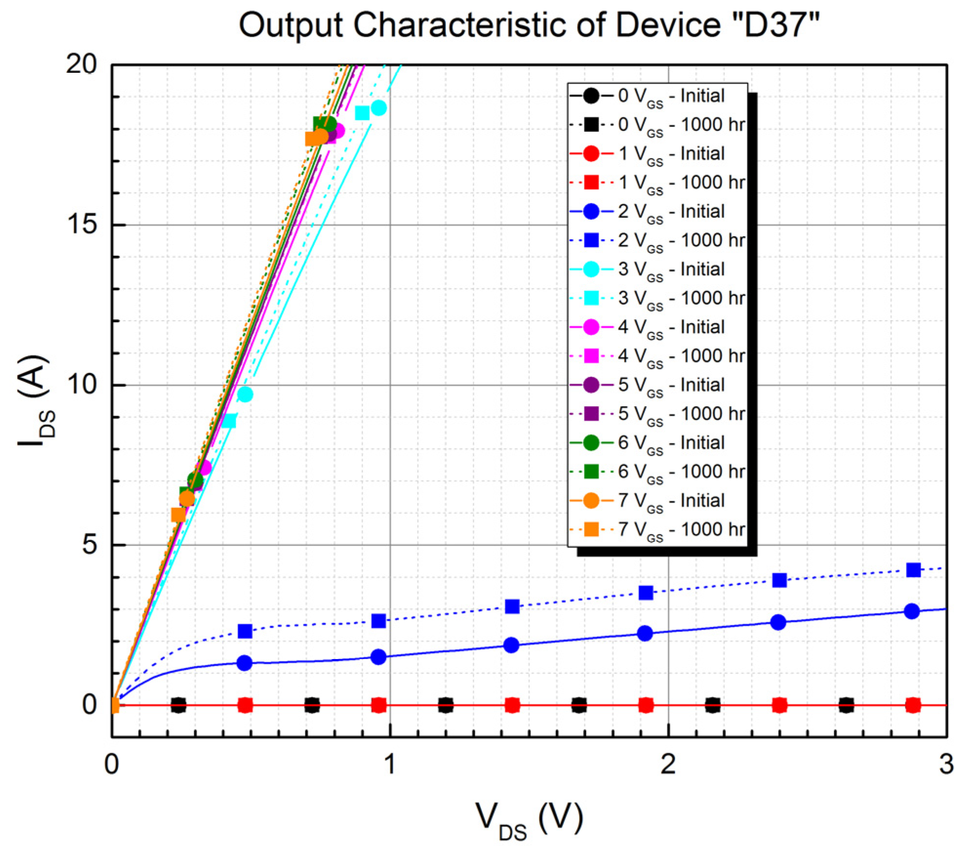
3. Results
4. Discussion
5. Conclusions
Author Contributions
Funding
Conflicts of Interest
References
- Lidow, A.; Strydom, J.; de Rooij, M.; Reusch, D. GaN Transistors For Efficient Power Conversion; John Wiley and Sons: West Sussex, UK, 2015. [Google Scholar]
- Guacci, M.; Anderson, J.A.; Pally, K.L.; Bortis, D.; Kolar, J.W.; Kasper, M.J.; Deboy, G. Experimental Characterization of Silicon and Gallium Nitride 200 V Power Semiconductors for Modular/Multi-Level Converters Using Advanced Measurement Techniques. IEEE J. Emerg. Sel. Top. Power Electron. 2020, 8, 2238–2254. [Google Scholar] [CrossRef]
- Jafari, A.; Nikoo, M.S.; Perera, N.; Yildirim, H.K.; Karakaya, F.; Soleimanzadeh, R.; Matioli, E. Comparison of Wide-Band-Gap Technologies for Soft-Switching Losses at High Frequencies. IEEE Trans. Power Electron. 2020, 35, 12595–12600. [Google Scholar] [CrossRef]
- Pushpakaran, B.N.; Subburaj, A.S.; Bayne, S.B. Commercial GaN-Based Power Electronic Systems: A Review. J. Electron. Mater. 2020, 49, 6247–6262. [Google Scholar] [CrossRef]
- Yang, W.; Yuan, J.-S.; Krishnan, B.; Shea, P. Characterization of Deep and Shallow Traps in GaN HEMT Using Multi-Frequency C-V Measurement and Pulse-Mode Voltage Stress. IEEE Trans. Device Mater. Reliab. 2019, 19, 350–357. [Google Scholar] [CrossRef]
- Hu, M.; Liu, G.; Du, E.; Mu, F. Thermal effect on dynamic Ron degradation of p-GaN AlGaN/GaN HEMTs on SiC substrates. IEICE Electron. Express 2020, 17, 20200255. [Google Scholar] [CrossRef]
- Ray, W.B.; Schrock, J.A.; Bilbao, A.V.; Kelley, M.; Lacouture, S.; Hirsch, E.; Bayne, S.B. Analysis of GaN power MOSFET exporsure to pulsed overcurrents. In Proceedings of the IEEE Pulsed Power Conference (PPC), Austin, TX, USA, 31 May–4 June 2015; pp. 1–5. [Google Scholar] [CrossRef]
- Li, H.; Li, X.; Wang, X.; Wang, J.; Alsmadi, Y.; Liu, L.; Bala, S. E-mode GaN HEMT short circuit robustness and degradation. In Proceedings of the IEEE Energy Conversion Congress and Exposition (ECCE), Cincinnati, OH, USA, 1–5 October 2017; pp. 1995–2002. [Google Scholar] [CrossRef]
- Song, Q.; Zhang, R.; Kozak, J.P.; Liu, J.; Li, Q.; Zhang, Y. Failure Mechanisms of Cascode GaN HEMTs Under Overvoltage and Surge Energy Events. In Proceedings of the IEEE International Reliability Physics Symposium (IRPS), Monterey, CA, USA, 21–25 March 2021; pp. 1–7. [Google Scholar] [CrossRef]
- Song, S.; Munk-Nielsen, S.; Uhrenfeldt, C. How Can a Cutting-Edge Gallium Nitride High-Electron-Mobility Transistor Encounter Catastrophic Failure within the Acceptable Temperature Range? IEEE Trans. Power Electron. 2020, 35, 6711–6718. [Google Scholar] [CrossRef]
- Cimmino, D.; Ferrero, S. High-Voltage Temperature Humidity Bias Test (HV-THB): Overview of Current Test Methodologies and Reliability Performances. Electronics 2020, 9, 1884. [Google Scholar] [CrossRef]
- Wang, N.; Cotton, I.; Evans, K. Impact of Thermal Cycling in Humid Environments on Power Electronic Modules. IEEE Trans. Compon. Packag. Manuf. Technol. 2012, 2, 1085–1091. [Google Scholar] [CrossRef]
- Qiu, L.; Guzonas, D.A.; Qian, J. Corrosion of silicon nitride in high temperature alkaline solutions. J. Nucl. Mater. 2016, 476, 293–301. [Google Scholar] [CrossRef]
- Deng, H.; Meng, J.; Wang, D.-B.; Zhang, W. Breakdown Voltage Impact on Lifetime of 1200V IGBT modules under H3TRB-HVDC Testing. In Proceedings of the IEEE 26th International Symposium on Physical and Failure Analysis of Integrated Circuits (IPFA), Hangzhou, China, 2–5 July 2019; pp. 1–4. [Google Scholar] [CrossRef]
- Hoffmann, F.; Kaminski, N.; Schmitt, S. Investigation on the Impact of Environmental Stress on the Thermo- Mechanical Reliability of IGBTs by Means of Consecutive H3TRB and PCT Testing. In Proceedings of the 2021 33rd International Symposium on Power Semiconductor Devices and ICs (ISPSD), Nagoya, Japan, 30 May–3 June 2021; pp. 371–374. [Google Scholar] [CrossRef]
- Zorn, C.; Kaminski, N. Temperature–humidity–bias testing on insulated-gate bipolar transistor modules—Failure modes and acceleration due to high voltage. IET Power Electron. 2015, 8, 2329–2335. [Google Scholar] [CrossRef]
- Dusmez, S.; Ali, S.H.; Heydarzadeh, M.; Kamath, A.S.; Duran, H.; Akin, B. Aging Precursor Identification and Lifetime Estimation for Thermally Aged Discrete Package Silicon Power Switches. IEEE Trans. Ind. Appl. 2017, 53, 251–260. [Google Scholar] [CrossRef]
- Brunko, A.; Gloth, M.; Kaminski, N. Humidity Capability of Enhancement Mode GaN High Electron Mobility Transistors. In Proceedings of the IEEE 8th Workshop on Wide Bandgap Power Devices and Applications (WiPDA), Redondo Beach, CA, USA, 7–11 November 2021; pp. 242–245. [Google Scholar] [CrossRef]
- Meneghini, M.; Hilt, O.; Wuerfl, J.; Meneghesso, G. Technology and Reliability of Normally-Off GaN HEMTs with p-Type Gate. Energies 2017, 10, 153. [Google Scholar] [CrossRef] [Green Version]
- Transphorm. TP65H035WS Datasheet. Available online: https://www.transphormusa.com/en/document/datasheet-tp65h035ws-650v-gan-fet/ (accessed on 22 April 2022).
- Nexpedia. GAN063-650WSA Datasheet. Available online: https://assets.nexperia.com/documents/data-sheet/GAN063-650WSA.pdf (accessed on 22 April 2022).
- GaN Systems. GS-065-030-2-L Datasheet. Available online: https://gansystems.com/wp-content/uploads/2021/08/GS-065-030-2-L-DS-Rev-210630.pdf (accessed on 22 April 2022).
- Transphorm. GaN for Automotive Applications. Available online: https://www.transphormusa.com/ja/document/autoreliabilityfaq-transphorm/ (accessed on 22 April 2022).
- Barr, R. Qualification Report TPH65H035WS. Available online: https://www.transphormusa.com/en/document/qualification-report-tp65h035ws/ (accessed on 22 April 2022).
- Ohring, M.; Kasprzak, L. Reliability and Failure of Electronic Materials and Devices Second Edition; Elsevier: Amsterdam, The Netherlands, 2014. [Google Scholar]
- Sigel, A.; Sigel, H.; Sigel, R.K.O. The Alkali Metal Ions: Their Role for Life; Springer: Berlin, Germany, 2016. [Google Scholar]
- Matsushima, H.; Yamada, R.; Shima, A. Two Mechanisms of Charge Accumulation in Edge Termination of 4H-SiC Diodes Caused by High-Temperature Bias Stress and High-Temperature and High-Humidity Bias Stress. IEEE Trans. Electron Devices 2018, 65, 3318–3325. [Google Scholar] [CrossRef]
- Natarajan, R.R.; Parthasarathy, E.; Murugapandiyan, P. Influence of High-k Passivation Layer on Gate Field Plate AlGaN/GaN/AlGaN Double Heterojunction HEMT. Silicon 2022, 14, 1–9. [Google Scholar] [CrossRef]
- Nezar, A.; Salama, C.A.T. Breakdown voltage in LDMOS transistors using internal field rings. IEEE Trans. Electron Devices 1991, 38, 1676–1680. [Google Scholar] [CrossRef]
- Efthymiou, L.; Murukesan, K.; Longobardi, G.; Udrea, F.; Shibib, A.; Terrill, K. Understanding the Threshold Voltage Instability During OFF-State Stress in p-GaN HEMTs. IEEE Electron Device Lett. 2019, 40, 1253–1256. [Google Scholar] [CrossRef]
- Tallarico, A.N.; Stoffels, S.; Posthuma, N.; Decoutere, S.; Sangiorgi, E.; Fiegna, C. Threshold Voltage Instability in GaN HEMTs with p-Type Gate: Mg Doping Compensation. IEEE Electron Device Lett. 2019, 40, 518–521. [Google Scholar] [CrossRef]
- Guo, H.; Gong, H.; Shao, P.; Yu, X.; Wang, J.; Wang, R.; Zheng, Y. Over 1200 V Normally-OFF p-NiO Gated AlGaN/GaN HEMTs on Si with a Small Threshold Voltage Shift. IEEE Electron Device Lett. 2022, 43, 268–271. [Google Scholar] [CrossRef]
- Habersat, D.B.; Lelis, A.J.; Green, R. Towards a Robust Approach to Threshold Voltage Characterization and High Temperature Gate Bias Qualification. In Proceedings of the IEEE International Reliability Physics Symposium (IRPS), Dallas, TX, USA, 28 April–30 May 2020; pp. 1–4. [Google Scholar] [CrossRef]
- Meneghini, M.; Rossetto, I.; Bisi, D.; Ruzzarin, M.; Van Hove, M.; Stoffels, S.; Zanoni, E. Negative Bias-Induced Threshold Voltage Instability in GaN-on-Si Power HEMTs. IEEE Electron Device Lett. 2016, 37, 474–477. [Google Scholar] [CrossRef]


| Device Parameter | Group “D1” | Group “D2” | Group “D3” | Unit |
|---|---|---|---|---|
| Part # | TP65H035WS | GAN063-650WSA | GS-065-030-2-L | |
| Blocking Voltage | 650 | 650 | 650 | V |
| Forward Current | 46.5 | 34.5 | 30 | A |
| On-state Resistance | 35 | 50 | 50 | mΩ |
| Threshold Voltage | 4 | 3.9 | 1.7 | V |
| Forward Current @ Vth | 1 | 1 | 10 | mA |
| Device Group | Failure Present | Affected Devices | Issue |
|---|---|---|---|
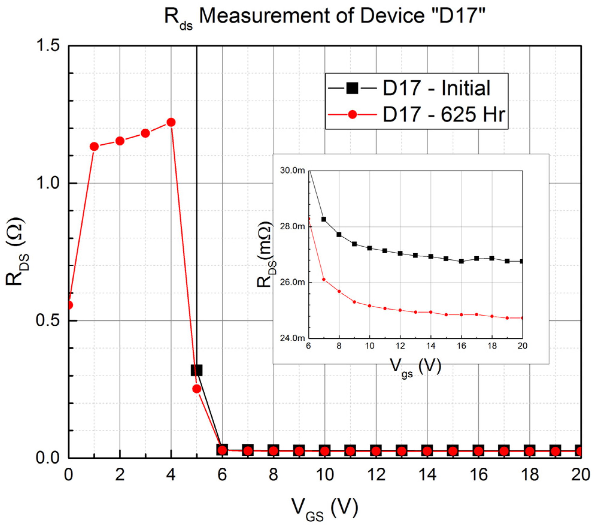
| D1 | Yes | D11, D13, D17 | Opened fuse |
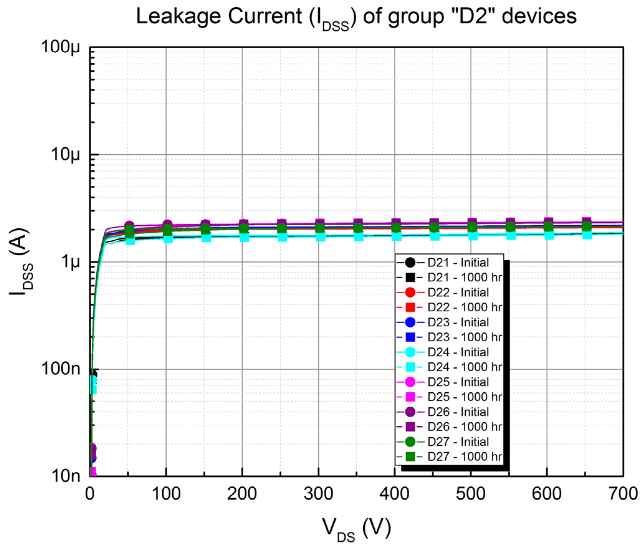
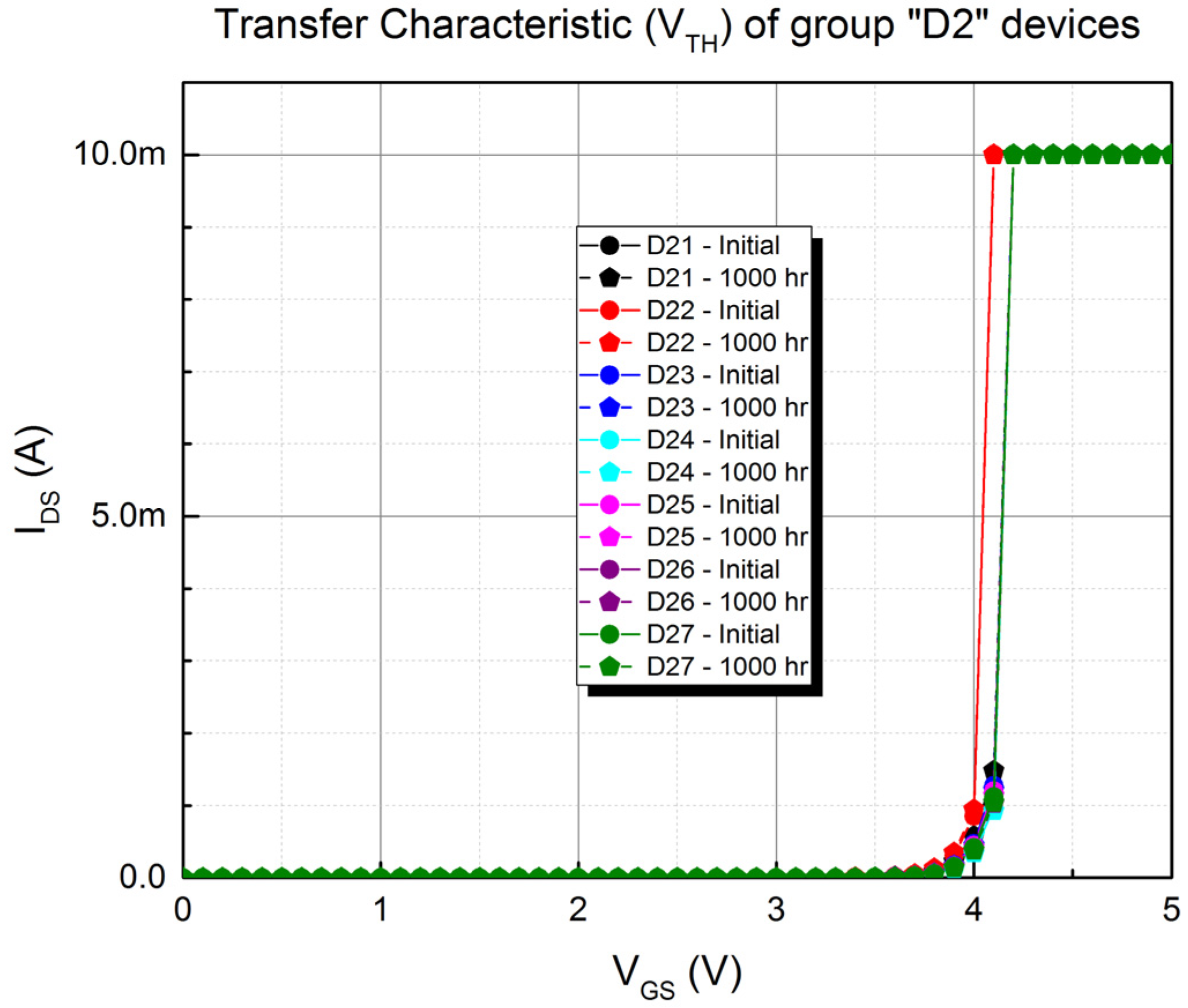
| D2 | No | None | None |
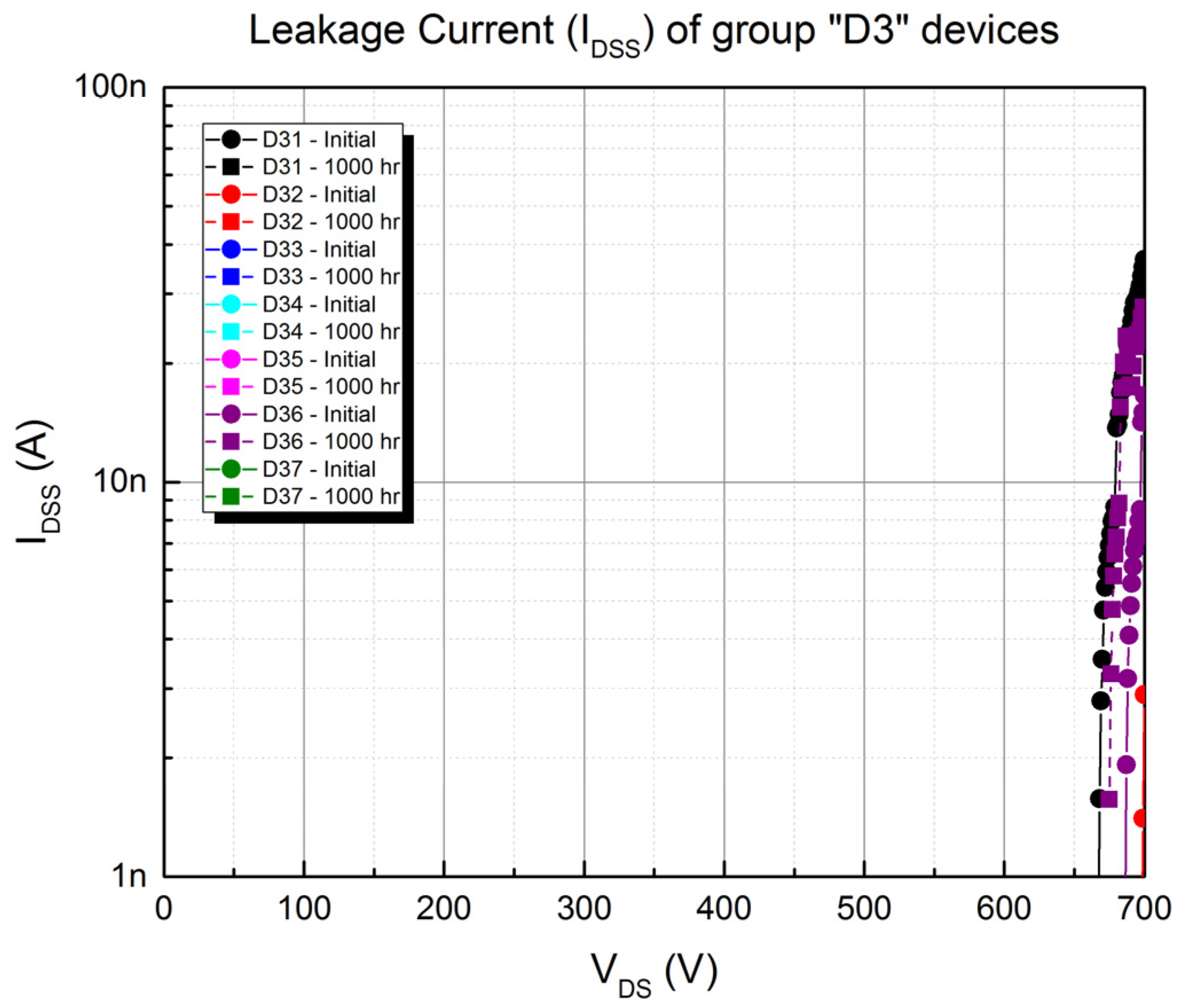
| D3 | No | None | None |
Publisher’s Note: MDPI stays neutral with regard to jurisdictional claims in published maps and institutional affiliations. |
© 2022 by the authors. Licensee MDPI, Basel, Switzerland. This article is an open access article distributed under the terms and conditions of the Creative Commons Attribution (CC BY) license (https://creativecommons.org/licenses/by/4.0/).
Share and Cite
Rodriguez, J.A.; Tsoi, T.; Graves, D.; Bayne, S.B. Evaluation of GaN HEMTs in H3TRB Reliability Testing. Electronics 2022, 11, 1532. https://doi.org/10.3390/electronics11101532
Rodriguez JA, Tsoi T, Graves D, Bayne SB. Evaluation of GaN HEMTs in H3TRB Reliability Testing. Electronics. 2022; 11(10):1532. https://doi.org/10.3390/electronics11101532
Chicago/Turabian StyleRodriguez, Jose A., Tsz Tsoi, David Graves, and Stephen B. Bayne. 2022. "Evaluation of GaN HEMTs in H3TRB Reliability Testing" Electronics 11, no. 10: 1532. https://doi.org/10.3390/electronics11101532
APA StyleRodriguez, J. A., Tsoi, T., Graves, D., & Bayne, S. B. (2022). Evaluation of GaN HEMTs in H3TRB Reliability Testing. Electronics, 11(10), 1532. https://doi.org/10.3390/electronics11101532