1. Introduction
ZYNQ-SoC is a hybrid architecture integrating embedded multi-processor cores (known as a programmable system) with the FPGA fabric (known as programmable logic). It combines the software flexibility of ARM processors with the parallel processing capability of reconfigurable hardware. Real-time low latency applications can be offloaded to the programmable logic. Unlike previous FPGAs with hard processors (for example, Virtex-Pro housing a PowerPC with FPGA fabric), the processing system (PS) in Zynq-SOC is fully capable and able to boot independently of the FPGA. Therefore, the programmable logic (PL) section is considered to be the auxiliary resource that can extend the processing capabilities when needed by designers. The PL portion of the ZynQ SoC can be partially and dynamically reconfigured during run-time under the control of the PS. This enables the ZynQ SoC to be deployed in self-healing and self re-configurable systems [
1].
For run-time reconfiguration in real-time systems, the generation of partial bitstreams and their size and delivery speed to the configuration memory are the factors to be considered. The compilation time for FPGAs is very slow due to the monolithic mapping process. For example, the Rosetta benchmark mapped onto Xilinx XCZU9EG FPGA takes 42 min [
2]. The reconfiguration time for recent FPGA families has been steadily increasing (i.e., in orders of several milliseconds [
3]) due to the increased density of the configuration memory (20 MB for Virtex-7) and unimproved throughput of the configuration interfaces [
4]. Compression techniques—for example, Huffman coding [
5] and difference vector (DV) [
6]—can be used to reduce the size of the bitstream. For incremental changes to the configuration memory—for example, changing the content of a single look-up table (LUT) or a Flip-Flop (FF)—direct bitstream manipulation can be used [
7]. There are important application domains in which high-speed fine-grain incremental configuration memory changes are vital, for example, fault injection in user and configuration memories [
4,
8]. fault injection requires huge amounts of time due to the extremely large input and fault space to explore. Vendor support for such application domains is limited, both in terms of the level of granularity of the reconfiguration they provide or their throughput.
For Zynq SOC, Xilinx provides software Application Programming Interfaces (APIs) for both the processor configuration access port (PCAP) and the internal configuration access port (ICAP) to access the configuration memory that imply flexibility but are unable to reach the maximum reconfiguration throughput. Compared to the theoretical bandwidth of 400 MB/s which is achievable with a 100 MHz clock and data width of 32 bits, PCAP reaches a throughput of 145 MB/s while Xilinx ICAP IP gives 19 MB/s. The PCAP can only be used with the PS, and its sole purpose is delivery from the PS to the PL of partial bit-streams stored in DRAM. The PCAP does not provide a software API for frame-level fine-grain reconfiguration [
9]. Custom ICAP controllers have been shown to achieve a throughput that is quite close to the theoretical limit; i.e., 380+ MB/s in some cases [
10,
11,
12,
13,
14,
15,
16,
17,
18,
19]. However, except for the author in [
16], no researchers support the fine-grain reconfiguration of primitive FPGA elements; e.g., LUTs. Even the author in [
16] does not support FF reconfiguration during run-time due to the challenges involved in avoiding unwanted state corruption [
4].
In this work, we propose a novel hardware-implemented reconfiguration controller featuring efficient control mechanisms that allow the run-time reconfiguration of LUTs and FFs. The main contributions of the proposed controller are its ability to support fine-grained LUT and FF reconfiguration at high speed with moderate resource usage. In particular, handling FF reconfiguration in run-time is not straightforward as it requires the safe assertion of the Global Set/Reset (GSR) line with side effects that can render logic in the static region corrupt if care is not taken. This is achieved with the usage of the reset after reconfiguration (RAR) feature offered in seven-series FPGAs. In our approach, first, a RAR bit-stream is downloaded upon system boot, which is accomplished through the PCAP. Therefore, our overall approach uses both the PCAP and the ICAP. However, the PCAP is used only once at the system boot. The proposed VR-ZyCAP controller provides the capability of on-the-fly LUT modification and the run-time reconfiguration of FFs in hardware. The proposed methodology is based on a ZynQ SoC architecture as it provides a single-chip processor–FPGA integrated solution, which is most suitable for applications such as fault injection. However, it can be adapted very easily to other Xilinx FPGA architectures. Our experimental results demonstrate that we can reconfigure LUTs and FFs at very high speeds compared to existing vendor-based software APIs [
4] or other state-of-the-art works. The same ideas can potentially be used for other vendors’ devices such as Intel’s Cyclone V SoC FPGAs. However, this is not considered in this paper and is left for future work.
The rest of the paper is structured as follows.
Section 2 discusses the motivation for fine-grained reconfiguration, describing several use cases in which it is needed.
Section 3 explains the architecture and configuration memory layout of Xilinx FPGAs.
Section 4 covers the literature review and provides an overview of the different reconfiguration controllers that have been developed over time.
Section 5 presents the proposed methodology.
Section 6 covers the experimental results and provides detailed comparisons with existing works.
Section 7 concludes the paper while also presenting some ideas for future work.
2. Motivation
Fine-grained reconfiguration has several applications in different domains. For example, it can be used in cryptography applications, where it can help in the design of countermeasure strategies [
16]. Another application domain is dynamic circuit specialization (DCS), where it can be used for updating adaptive filters in run-time; for example, as outlined in [
12]. In general, it is applicable to systems with user parameters that can change during run-time; however, the rate of change of these parameters should be orders of magnitude slower than the system operating frequency, meaning that these parameters should change less frequently. In such cases, fine-grained reconfiguration is useful as it avoids the lengthy partial bitstream generation of vendor design flow. To illustrate the potential use of fine-grained reconfiguration, this section briefly discusses three practical applications that benefit from the fine-grained reconfiguration of LUTs and FFs in more detail. These applications assume a system in which a processor and a programmable logic are present, as is the case with our proposed VR-ZyCAP controller.
2.1. FPGA-Based Ternary Content Addressable Memories
With the rise of programmable dataplanes in software-defined networking (SDN), FPGA-based ternary content addressable memories (TCAMs) have received a great deal of interest. As there is no built-in macro for its implementation in modern SRAM-based FPGA, TCAM has to be emulated using on-chip logic and memory resources. PR-TCAM [
20] represents one interesting approach, implementing a TCAM using logic LUTs in contrast to the memory LUTs used traditionally. The logic LUTs are combinational in nature and can only be updated using reconfiguration during run-time. VR-ZyCAP is an ideal platform to achieve such fine-grained LUT-level reconfiguration for PR-TCAM. The PS algorithm is responsible for identifying which LUTs need to be modified with new configurations (i.e., rules). This is controlled by the user. Once the physical location of a LUT and updated rule values are passed to VR-ZyCAP, it reconfigures the corresponding LUT in run-time. The newly updated rules can be easily verified by passing a key value from the PS to PL and checking the received match signal. This fine-grained partial reconfiguration would speed up TCAM rule modifications compared to existing approaches, making the PR-TCAM rule update speed competitive. It is worth noting that, without fine-grained reconfiguration, the modification of PR-TCAM rules is not practical as the vendor partial reconfiguration flow for generating a partial bitstream for smallest Pblock (i.e., 2 CLB columns in seven-series FPGAs) is more than three minutes, while for our approach, the read–modify–write cycle on the embedded platform requires a time consumption on the order of a few milliseconds at worst. In order to update a rule in PR-TCAM, multiple LUTs across different CLB columns may be involved, which would require a huge amount of compilation and partial bitstream generation time in addition to the memory required for storage on the embedded platform. Therefore, it is not feasible to implement PR-TCAM with the vendor partial reconfiguration flow.
VR-ZyCAP can be also used with G-AETCAM [
21], which stores its rules in the FPGA FFs. In fact, G-AETCAM [
21] needs logic to modify FFs, which can be removed if the FFs are updated through the FPGA configuration layer through VR-ZyCAP. This would make G-AETCAM [
21] more efficient in terms of resource usage and can accelerate the FF content modification in real-time, with very high speed compared to existing FF reconfiguration approaches.
2.2. Design of Fault Tolerant FPGA-Based CNNs
Convolutional neural networks (CNNs) are widely used, for example, in computer vision, speech recognition and natural language processing (NLP). When the application domain is a safety-critical system—for example, in automotive, avionics or space industries—reliability becomes an important requirement [
22,
23]. Reliability evaluation and fault-tolerant design for FPGA-based CNNs have recently received a great deal of interest from researchers [
24,
25,
26]. The proposed VR-ZyCAP can enable soft error injection in user memories as well as configuration memory [
26]. The information of FFs to be modified is passed from the PS to the PL through the logic allocation (LL) file. In order to flip the value of an FF, it first needs to be captured. The clock is stopped in the device-under-test (DUT) region. The current value of the FF is captured in the configuration memory. Then, the FF corresponding configuration memory is bit-flipped. Next, the DUT region is unmasked and the static region is masked to avoid unintentional state changes in other FFs before the configuration memory is written. VR-ZyCAP is ideal for this application, and its DPR FF flow considers all the requirements of FF modification in run-time. The fault injection speed is a critical factor as CNNs are large and thus the number of faults to test is also very large. VR-ZyCAP will help in speeding up CNN testing.
As FPGAs are also increasingly used in safety-critical applications and the testing and qualification of such systems become more stringent, evaluating the impact of errors on FFs will be necessary. For example, for electronic automotive systems, the ISO-26262 standard already defines functional safety requirements that need to be met and mandates the testing of the effect of errors on the components.
2.3. Side Channel Attacks Protection
Side channel attacks (SCA) are one of the latest threats to computer systems in which an attacker tries to break a cryptographic implementation by launching attacks based on system properties such as its power consumption, heat signature, timing information, etc. [
27]. The attacker does not target the weaknesses of the cryptographic algorithm but rather the weaknesses that may have been introduced by the programmer of the system due to a lack of knowledge or poor coding practices. Securing modern SRAM-based FPGA implementation against such attacks is an active research area. One possible counter-measure against such attacks can be realized using fine-grained dynamic partial reconfiguration (DPR) such as the one provided by the proposed VR-ZyCAP.
Consider the example of the integrity calculation cryptographic hashing algorithm, the Secure Hashing Algorithm (SHA), which is considered to be the de-facto hashing standard. In each variant of SHA (1, 2 and 3) the algorithm is initialized with some round constants that thwart an attack based on data symmetry. If a system contains an implementation of the SHA algorithm with some fundamental vulnerability that may have been introduced as a result of poor user implementation, then it can help an attacker to launch a series of attacks on the SHA algorithm.
Now, consider a system that contains “N” different implementations, instead of one implementation of the SHA algorithm, that is available on the PS side that and can be loaded on-demand to the PL via VR-ZyCAP. All of these implementations have the common property that initial round constants values are stored in FFs on the PL side, which can be accessed from the PS side and can be updated dynamically. In order to mask the result of hash computation against SCA, a user can switch the SHA implementation seamlessly by selecting one of many SHA implementations available at the disposal of PS, form a run-time partial bit-stream and deliver it using the proposed VR-ZyCAP, dynamically switching from one implementation to another, thus causing a great deal of confusion for an attacker that aims to determine the power traces of a system. Before replacing SHA algorithm-1 with SHA algorithm-2, intermediate calculation results of SHA algorithm-1 have to be captured using DPR, and once SHA algorithm-2 is successfully loaded using DPR, the initial round constants of SHA algorithm-2 have to be replaced with the intermediate calculation results of SHA algorithm-1. Thus, no intermediate results are lost while achieving protection against SCA using DPR. To make this possible, fine-grained reconfiguration of FFs is needed. Finally, the selection of the next SHA implementation out of “N” implementations may be done using a true random number generating system to avoid bias.
The proposed method not only provides better protection against SCA but also eliminates the need for lengthy off-chip bit-stream creation using IDEs such as Xilinx ISE or Vivado which take at least a couple of minutes [
9]. Those large times would make the described protection impractical, as time is often of great importance in extensive computation algorithms, including but not limited to hashing, encryption, asymmetric key-pair generation and key-exchange, etc. VR-ZyCAP would make protection using several implementations of the algorithm during run-time feasible.
3. FPGA Structure and Reconfiguration of LUTs and FFs
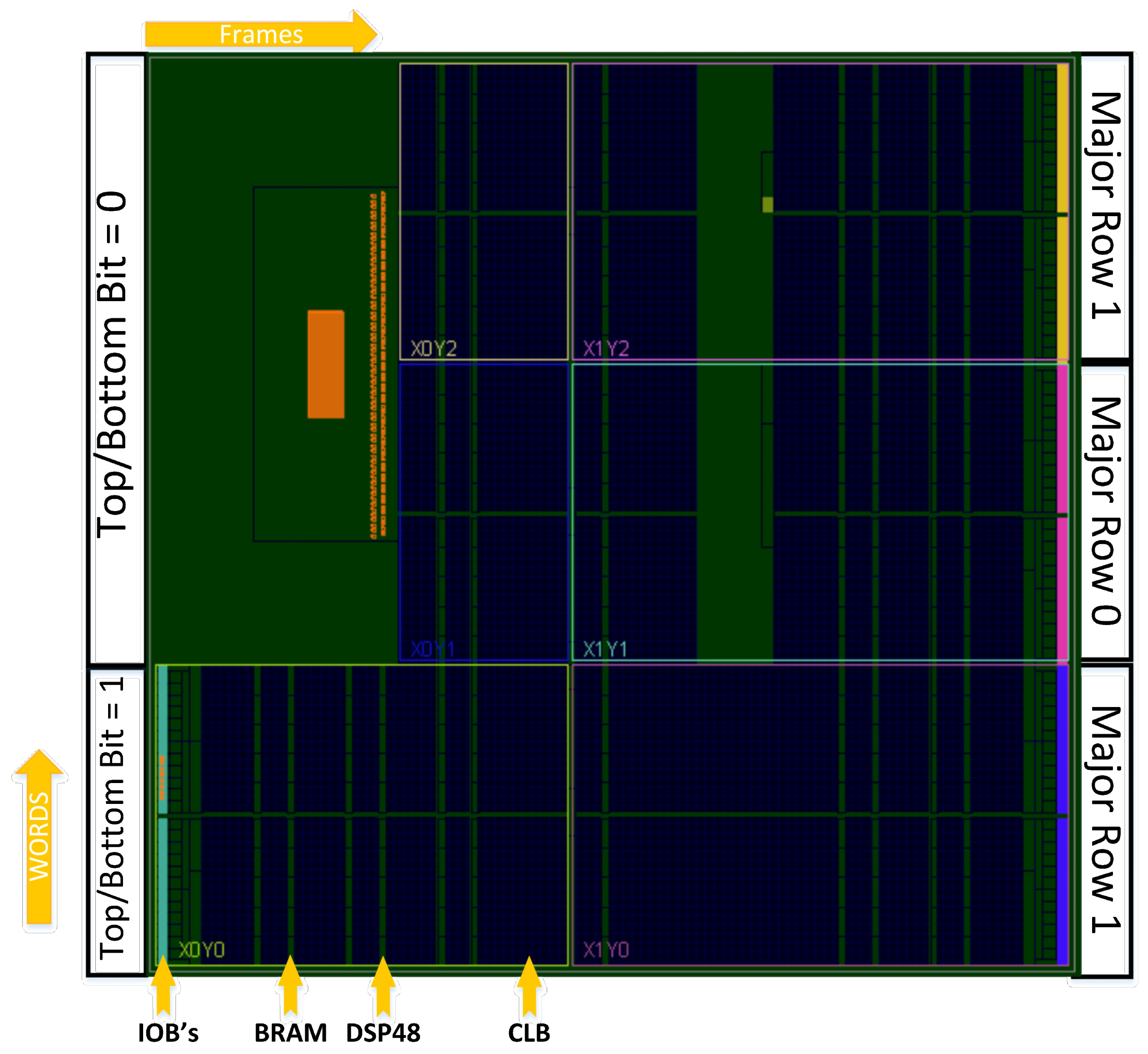
This section discusses the architecture of the ZynQ SoC; however, it should be noted that the proposed controller is applicable also to seven-series FPGA devices and their configuration memory in general as ZynQ SoCs are a combination of ARM Cortex-A9 cores in the PS with Artix-7 FPGA in the PL, as shown in
Figure 1. The FPGA architecture consists of columns of different resources, such as input output blocks (IOBs), configurable logic blocks (CLBs), digital signal processors (DSPs), block RAMs (BRAMs) and clock management tiles (CMTs), etc. The FPGA device is divided horizontally into two halves; i.e., the top half and the bottom half, represented by TOP/BOTTOM bit = 0 and TOP/BOTTOM bit = 1, respectively.
In each half, there can be several horizontal clock (HCLK) rows depending upon the family and part. For example, in ZynQ SoC(ZC07020) with an integrated Artix-7 FPGA, three HCLK rows (also called major rows) are present in the PL section, as shown in
Figure 1. The HCLK/major rows start in the middle of the device with an ID of zero, and IDs are incremented along the top half and also along the bottom half. The height of an HCLK row is equal to the CLB column (i.e., 50 CLB), and the width is the same as the device width. An HCLK is further divided into two halves by the regional clock resources: 25 CLBs above the clock routing and 25 CLBs below. An HCLK row contains different numbers of CLBs, BRAM, DSP and I/Os depending on the width of a device. There are 400 LUTs per CLB column, where each CLB column is 50 CLB high, resulting in eight LUTs per CLB. As each CLB has two slices—even and odd—there are four LUTs per slice.
LUTs in the seven-series architecture are used to implement six-input arbitrary Boolean functions that require a 64-bit initialization value. Each six-input LUT can also be used as a dual five-input LUT with shared inputs. From a reconfiguration perspective, the 64 bit configuration for a six-input LUT is divided into two 32-bit groups, with one for each five-input LUT. One must know the location of the logic resource in the configuration memory space in order to dynamically reconfigure a system at run-time. There are two types of locations associated with a LUT; i.e., its location in the XY coordinate system and its location in the configuration memory represented by a 32-bit frame address register (FAR). The LUT location can be specified in a constraint file in UCF or XDC format as the XY coordinates of the target slice, which can then be mapped to the configuration memory at the corresponding frame address; i.e., the FAR. The format of the LUT location is defined as a pair of (X,Y) and BEL, where X determines the row, Y determines the column of a slice and BEL defines the LUT position within that slice; i.e., LUTA, LUTB, LUTC or LUTD.
Figure 2 illustrates the configuration memory layout of a CLB column which represents both our elements of interest—i.e., LUTs and FFs—in the configuration space. This CLB column has 36 minor frames (or just frames) where a frame is the smallest unit of configuration memory that can be addressed. Each frame has 101 words, where each word is 32 bits. Thus, each frame contains 3232 (101 × 32) bits which are stored in SRAM cells. In order to understand the relationship between the mapping of logic resources in a CLB column and its configuration memory, consider the ODD slice in
Figure 2. It can be seen that the configuration words start at the bottom with “word0” and move up to “word100” at the top of the CLB column in the configuration space. As annotated in this figure, one can see the Y coordinate of the slice in which our LUTs are mapped. Note that for “Y0” at the bottom, two words are required to configure its LUTA, LUTB, LUTC and LUTD across frames 26, 27, 28 and 29. It can be seen that “word0” contains 16 bits of LUTA and 16 bits of LUTB. Similarly, “word1” contains configuration data for 16 bits of LUTC and 16 bits of LUTD. Therefore, if we consider a single LUT (i.e. LUTA, LUTB, LUTC, LUTD), its 64 bits span over four frames. The same pattern is used for even slices, but the minor frames are different; i.e., 32, 33, 34 and 35. Therefore, 100 words are required for the configuration of 50 CLBs. One word in the middle of the frame—i.e., word 51—is for clock information and the error correction code [
28]. Thus, the 400 LUTs in a CLB column are configured by 100 words spanning four frames in the pattern shown in
Figure 2. With minor differences across the Xilinx FPGA families, the frame layout largely remains the same; for example, the layout presented here is the same as that of Virtex-5 except for the number of CLBs in a column or the corresponding words. The major column determination for the XY LUT location is further discussed in the proposed methodology section.
Figure 2 shows that frame 31 contains data for the FFs of the CLB. There are different frames for even and odd slices. These frames contain the instantaneous data for FFs as well as their configuration settings. However, an exact decoding and mapping between FFs in the logic space and configuration space is not difficult, as the logic allocation (LL) file generated by Xilinx design tools gives the locations of all the FFs in the configuration address space. The initialization of a FF to a known state is interesting to look into from a FPGA architecture perspective. This is achieved by setting the initial values of FFs in HDL, which are mapped and stored in the bit-stream and downloaded to the FPGA upon first configuration.
Figure 3 shows the logic that is used for this purpose. It can be seen that each slice FF is shadowed by another extra FF (it can be a transistor-level optimized memory element other than a FF). The shadow FF receives the initialization contents from the bit-stream during the download process. After this, a global set/reset (GSR) command sequence initializes all the FFs in the FPGA from these shadow FFs. If the user wants to know the instantaneous value stored in a FF, which represents the current state of the system mapped onto the FPGA, the user can trigger a global capture (GCAP) signal which will save the state of all the FFs in the shadow memory. This state can then be retrieved through configuration memory, read back and changed to the desired value [
4]. However, to reliably reconfigure FFs, before triggering the GCAP, the clock to the FFs should be stopped. The FPGA architecture is designed such that all the memory elements are connected to the same GSR and GCAP. This has the implication that if a system is divided into static and dynamic regions, the triggering of GSR and GCAP should not affect the static region. This problem is handled with the reset after reconfiguration (RAR) partial bitstream in [
4], which masks the GSR and GCAP signals in the static design while unmasking them in the dynamic/reconfigurable region. It should be kept in mind that the global signals are asynchronous signals and may cause timing violation when triggered in run-time. Therefore, care must be taken to allow transitions on these signals to settle by allowing adequate time.
4. Related Work
This section discusses several existing reconfiguration controllers and analyzes and compares their performance in terms of their reconfiguration time, resource usage and throughput. Hardware resource utilization and reconfiguration time are often considered to be the two main performance metrics of a reconfiguration controller. A trade-off between these two is required to get an optimized solution.
Vendor-provided reconfiguration controllers are mostly dependent on a processor. Software APIs are used to access the configuration memory, such as OPB HwICAP [
19], XPS HwICAP [
29] and AXI HwICAP [
30]. The speed of these reconfiguration controllers is limited by the interconnecting bus interface with which the ICAP is connected. OPB HwICAP offers a low communication bandwidth between the processor and the ICAP, which is around 4 MB/s; that is, 100 times slower than the theoretical bandwidth of the ICAP (400 MB/s) [
19]. Similarly, XPS HwICAP provides 10 MB/s data throughput and only supports Microblaze and Power PC processors in Virtex 4, Virtex 5, Virtex6 and Spartan 6 [
29]. AXI HwICAP is used in seven-series architectures and above that support resource and long frame reading. Functionality to read/write CLBs, LUTs and FFs is also supported using software APIs. Due to the complex architecture and low processor communication bandwidth, this type of ICAP controller has a low bandwidth of approximately 19 MB/s [
30]. The architecture of XPS HwICAP and AXI HwICAP is similar, resulting in the same resource utilization, with the only difference being the reconfiguration throughput and bus latency.
Another type of reconfiguration controller is based on the ZynQ device. Besides the internal configuration access port (ICAP), ZynQ devices are also equipped with a novel configuration interface that supports dynamic partial reconfiguration (DPR), called PCAP. The main advantage that PCAP provides is the transfer of partial bit-streams through the DMA engine from external memory such as an SD-card or DRAM to read/write configuration FIFOs over the AXI-PCAP bridge [
9]. PCAP can operate at a maximum clock frequency of 100 MHz with a 32-bit data width, thus having a maximum physical bandwidth of 400 MB/s [
31]. However, the maximum bandwidth of PCAP is limited to 145 MB/s [
32] due to the limitations of the PS AXI–bus interface. In [
10], the authors proposed the idea of connecting the AXI HwICAP to the hard DMA controller to transfer partial bit-streams from external memory, which can significantly improve data throughput from 19 MB/s to 67 MB/s. The ZyCAP controller introduced in [
10] also achieves an increased reconfiguration throughput of up to 382 MB/s by the addition of the AXI-4 interface which is connected to high-performance (HP) ports to transfer partial bit-stream data through a soft DMA controller. Finally, the MiCAP and MiCAP-Pro are also Zynq-based reconfiguration controllers presented in [
11] in which an efficient state machine is utilized to deal with the slow reconfiguration speed mentioned in AXI HwICAP. MiCAP-Pro is the advanced version of the basic MiCAP in which the reconfiguration throughput is increased up to 272 MB/s by the addition of a DMA engine and an HP port. Another partial reconfiguration controller (PRC) mentioned in [
13] has microblaze processor-based architecture instead of ZynQ. At one time, two words of bitstream can be sent due to the 64-bit data width of the bus, which makes it very fast. Furthermore, separate FIFOs for read and write frames are utilized with a minimum depth of 16 64-bit words, which also helps in reducing the resource area. However, it does not have read-back capability and resource-level reconfiguration. A tiny ICAP controller is presented in [
15] which utilizes Picoblaze to read and write frame data into dual port memory. The size of memory is kept at one frame and the reading and writing of frames is performed using C functions in Picoblaze; thus, resource utilization is significantly reduced. The purpose of this controller is to check the status of the configuration registers; thus, it has read-back capability.
Some Reconfiguration controllers are designed completely in hardware and are independent of the processor; for example, DyRACT [
14] and RT-ICAP [
17]. DyRACT [
14] uses the PCIe interface in conjunction with the ICAP to transfer partial bit-streams of larger sizes, thus giving a high communication bandwidth that results in a high data throughput of up to 364 MB/s and an improved reconfiguration time. In the RT-ICAP controller [
17], the reconfiguration time is reduced by using scratch pad memory (SPM), but the limitation is the size of the SPM. If the partial bit-stream fits into the SPM, then maximum reconfiguration throughput can be achieved. Bitstream compression techniques are also used to reduce the configuration data size so that a reconfiguration throughput of up to 382.2 MB/s is achieved.
All the reconfiguration controllers discussed above achieve high reconfiguration throughput at the cost of increased hardware usage. Some efforts have also been devoted to increasing reconfiguration throughput by increasing the ICAP clock up to 500 MHz above the recommended clock frequency. The maximum reconfiguration throughput achieved is up to 2200 MB/s at 500 MHz clock frequency [
33].
Most of the reconfiguration controllers discussed in this section aim to deliver partial bit-streams in less time, but only a few reconfiguration controllers exist which have read-back capability. This small group includes the AC_ICAP controller introduced in [
16], which not only sends the partial bit-stream with high reconfiguration throughput but also provides the additional functionality of the run-time reconfiguration of the LUTs. This reconfiguration controller is completely implemented in hardware, so additional hardware resources are utilized compared to the reference design, but the reconfiguration speed is 380 times faster [
29]. However, even AC_ICAP [
16] does not support FF reconfiguration during run-time. Our proposed reconfiguration controller VR-ZyCAP supports both LUT and FF reconfiguration with very high speed, as presented in the next section.
5. Proposed VR-ZyCAP Controller
The proposed VR-ZyCAP is based on the ZynQ SoC and is able to reconfigure LUTs and FFs during run-time at a fine-grained level. It differs from most of the existing reconfiguration controllers as they are designed for coarse-grained module-level reconfiguration. It accelerates the process of LUT and FF reconfiguration while keeping the static logic intact. The acceleration is achieved by entirely handling the LUT and FF reconfiguration in hardware while the static logic is being masked. This masking is achieved by generating a partial bitstream with particular settings, which is first downloaded into the FPGA with the processor configuration access port (PCAP), and then continuing the LUT and FF reconfiguration during run-time with the ICAP configuration ports. This usage of the PCAP enables the design of a controller that loads a partial bitstream from external memory to be avoided, which in our case is required only once. Partial bitstreams for the configuration of LUTs and FFs are not pre-generated but instead are created during the read–modify–write (RMW) cycle of the ICAP at run-time by the proposed VR-ZyCAP. This avoids the lengthy compilation of FPGA design tools.
The rest of this section covers the computer-assisted design (CAD) flow and PS-PL mapping of the VR-ZyCAP (the source code of the controller is open source and is available at
https://github.com/bushra-sultana/VR-ZyCAP, accessed on 10 September 2020) onto the ZynQ SoC as shown in
Figure 4. The main components of the platform are the CAD flow, the PS algorithm and the PL logic of VR-ZyCAP (which consists of different modules performing two main operations: DPR–LUT and DPR–FF). The main contribution of VR-ZyCAP is two-fold: the support of the dynamic partial reconfiguration of LUTs (DPR–LUT) and of the dynamic partial reconfiguration of FFs (DPR–FF). The latter is realized by a novel hybrid approach, combining the read-back, capture and masking capabilities of seven-series FPGAs. DPR–LUT and DPR–FF functionality is implemented in the ZynQ-PL section, which is realized using Verilog HDL, while the masking is achieved via the ZynQ PS realized using C language. Our proposed VR-ZyCAP uses the AXI interconnection to establish communication between ZynQ PL and PS. Run-time manageable parameters are provided to VR-ZyCAP using general purpose input/output pins (GPIOs).
Figure 4 shows the complete design architecture of VR-ZyCAP. From
Figure 4, it can be seen that our VR-ZyCAP reconfiguration controller and device under test (DUT) are implemented on the ZynQ-PL side, whereas the C code runs on the ZynQ PS. The following sub-sections discuss this in more detail.
5.1. CAD Flow
Tools such as those in [
34,
35,
36] offer advanced floor-planning and constraint generation during design flow and bitstream manipulation phases [
37]. However, our approach utilizes the standard Xilinx flow as we only need to mask the static region and unmask the reconfigurable region which is available in a reset after reconfiguration (RAR)-supported partial bitstream. Furthermore, we are interested in reconfiguring LUTs and FFs at the fine-grained level, while the above tools are appropriate for more complex partial reconfiguration of entire modules, and when considered to be used during run-time on an embedded platform such as ZynQ SoC, they may add overheads in terms of memory footprint and processing cycles, while utilizing them off-line is not suitable for the applications under consideration. In our controller, on the other hand, we map all DPR–LUT and DPR–FF functionalities in hardware on the FPGA fabric to make them extremely fast for applications that need fast fine-grained reconfiguration. Furthermore, tools such as that in [
37] offer DPR–LUT functionality, but there are no software APIs to handle DPR–FFs directly. Therefore, we have developed our own hardware–software solution to support these features; more details are presented in the following sub-sections.
5.1.1. Generating a RAR Bit-Stream
The reset after reconfiguration property initializes re-configurable regions to their starting known values while static routes can easily pass through the re-configurable region [
38]. This property can only be applied on Pblocks, so Pblock constraints must align to re-configurable frames and must also be aligned vertically to the clock region [
38]. We applied this property to DUT_Pblock; the area selected was between slices X0Y0 and X7Y49.
5.1.2. Generating Logic Allocation (LL) File
The logic allocation (LL) file helps to determine the physically mapped logic positions of FFs, BRAMs and I/Os within the FPGA. This file can be optionally generated by turning on the relevant flags in Vivado IDE during the bit-stream generation process. The LL file can be used to determine the frame address within the configuration memory and the bit position of an FF.
5.1.3. SD Card Content
We used an SD card due to its non-volatile nature to store the RAR partial bit-streams. SD card drivers are available within the Xilinx Software Development Kit (SDK). At system power-up, the DDR memory and the SD card are initialized. Following this, the partial bit-stream is read from the SD card and transferred to the DDR memory at our pre-specified address.
5.2. PS Algorithm for VR-ZyCAP
The PS algorithm is responsible for the operations at the startup of the ZynQ SoC as represented by Algorithm 1. It can be seen that the algorithm is responsible for the initialization of all the drivers of the system; i.e., the IPs in the PS and in the PL. It also loads the RAR partial bit-stream from the SD card to the FPGA fabric. This is very important for the dynamic reconfiguration of FFs and is necessary to avoid the corruption of static logic in the PL. RAR configuration is done to mask the static region and unmask the re-configurable region during the process of DPR. The resulting partial bit-stream for DUT is loaded to configuration memory using the RAR_reconfiguration() function. This function is developed in the Xilinx SDK for the ZynQ PS. This function uses software APIs to load partial bit-streams to configuration memory using the PCAP interface. First, it transfers the partial bit-stream from the SD card to the DDR memory, and from there it loads it into the PL through the PCAP. The device configuration (DCFG) interface is utilized to transfer bit-stream data onto the configuration memory using the PCAP. Bit-stream location and size are the two important parameters to send the appropriate configuration data to the PL. The PCAP utilizes software APIs (XDcfg_Transfer()) to load the partial bit-stream to the configuration memory. The system then switches from the PCAP to the ICAP as the configuration engine is shared by both interfaces. This switching will last for the rest of the operation of the system as VR-ZyCAP is used for dynamic reconfiguration of LUTs and FFs. The algorithm also controls the main FSM in the VR-ZyCAP by communicating important setup parameters through AXI-compatible interfaces. The user-defined
value is received through PS UART and controls the
,
,
,
and
functions. It should be noted that after
, the system should wait for any transients of the GSR line to settle down, otherwise this asynchronous line can cause a timing violation. Therefore, a delay is introduced to cope with these effects. Furthermore, the read/write frames are handled by an on-chip BRAM, and therefore the PS function does not show them. The PL logic is exposed to the PS algorithm as memory-mapped AXI-connected peripherals controlled through general purpose input–output (GPIO) IPs.
| Algorithm 1: PS algorithm |
| Input: OP_done |
| Output: Start, Rst, Op_Sel, Start_Addr, XYBEL, Num_frames, Bit-Location, |
| Mem_Addr |
| Next_Option = inbyte(); |
| Switch(Next_Option) |
| case(0): |
| Driver_Init(); |
| RAR_Configuration(); |
| Switch_from_PCAP_to_ICAP(); |
| case(1): |
| OP_Sel = inbyte(); |
| Start_Addr = inbyte(); |
| Num_frames = inbyte(); |
| Read_frame(OP_Sel, Start_Addr, Num_frames); |
| case(2): |
| OP_Sel = inbyte(); |
| Start_Addr = inbyte(); |
| Num_frames = inbyte(); |
| Write_frame(OP_Sel, Start_Addr, Num_frames); |
| case(3): |
| OP_Sel = inbyte(); |
| XYBEL = inbyte(); |
| INIT = inbyte(); |
| DPR_LUT(OP_Sel, XYBEL, INIT); |
| case(4): |
| OP_Sel = inbyte(); |
| Start_Addr = inbyte(); |
| Bit-Location = inbyte(); |
| DPR_FF(OP_Sel, Bit-Location, Strat_Addr); |
| wait_for_GSR(); |
| case(5): |
| OP_Sel = inbyte(); |
| Start_Addr = inbyte(); |
| Read_BRAM(OP_Sel, Mem_Addr); |
| endcase |
5.3. Datapath and FSM for VR-ZyCAP
The architecture of the PL of the VR-ZyCAP controller is modular, with different sub-modules along with logic components and device primitives in DPR_LUT and DPR_FF, as shown in
Figure 4. The sub-modules in the PL part of the VR-ZyCAP architecture are described below.
5.3.1. Read Frame
The read frame module requires two inputs to read any PL frame; and (number of frames). determines the frame address (FAR) from where data should be read. input increments automatically up to the specified input. may be greater than one but less than or equal to the total available memory space of the BRAM memory. To read multiple frames, the size of the BRAM memory must be considered. It should be noted that the number of frames must include a dummy frame (to be specified in the configuration register (FDRO)) before reading from configuration memory. Therefore, to read back the entire contents of a single LUT, the total number of frames must be specified as four data frames and one dummy frame. When performing a read operation on seven-series FPGA configuration memory, a dummy frame is always read first followed by the desired data frames.
When reading an FPGA frame data using the ICAP, a correct assertion of the chip enable (CE) and read/write (RDWR) signal is of paramount importance. The CE signal controls the read and write operation over the ICAP. The RDWR signal is asserted as low when a write to configuration commands is desired and asserted as high when performing configuration memory read-back is required, as shown in
Figure 5. When the ICAP is in an active state, RDWR signal logic state cannot be changed from read to write or vice versa. Only upon the correct assertion of CE and RDWR are configuration commands sent to the ICAP. These signals are also shown in
Figure 5, which summarizes the read and write commands.
We can see from
Figure 5 that read-back operation starts when dummy words followed by the SYNC word (0xAA559966) are sent over ICAP. Upon receiving the SYNC word, the ICAP output changes from 0xFFFFFF9B to 0xFFFFFFDB, which indicates that the ICAP is configured successfully. After this, the processing of subsequent data words begin from the FDRO register (Type-2 read). The ICAP session can be terminated through a de-SYNC command, after which no further data are accepted. If another frame read-back is desired, the read process will have to start again from the beginning. The configuration commands were adopted from seven-series configuration user guide [
39]. The process for reading the contents of FF differs slightly from the LUT reading. For a successful reading of an FF, the clock of the FF must be stopped prior to capturing (using the CAPTURE primitive) the instantaneous value of the FF, as shown in
Figure 3.
5.3.2. Write Frame
The write frame module has two inputs;
and
. The write frame FSM is a bit more complex than the read frame due to the inclusion of additional configuration commands, as shown in
Figure 5. These commands are needed when writing data to the configuration memory. The primary commands for the write frame are the same as in the read frame FSM, with the difference being that, after the initialization of the ICAP, the device ID code must be written in the IDCODE register. After that, the frame address is sent in the frame address register. The write configuration command (WCFG) directs the ICAP to write configuration data using the FDRI register. It must be noted here that, while writing configuration data, a dummy frame must be appended at the end to flush the configuration register, as opposed to the configuration memory read-back process. Once the configuration data have been sent, the CRC value of the frame is computed and written to the CRC register. The FPGA internal configuration memory controller then compares the received CRC values against the CRC value computed during bit-stream reception. If both values are not a perfect match, the configuration process aborts [
39].
The FPGA startup sequence begins after a successful CRC check which performs various tasks including releasing control of the FPGA done pin, activating the I/O and the assertion of the chip wide global write enable (GWE) signal to change the state of synchronous elements [
39]. Similar to the read frame, the write frame must also be terminated by a de-SYNC Command. During our testing, it was observed that upon the assertion of the De-SYNC command, the ICAP output changes from 0xFFFFFFDB to 0xFFFFFF9B and it takes six additional clock cycles to complete the process. The Vivado design suite allows the CRC check in the bit-stream generation setting to be bypassed to allow continuous operation; therefore, CRC checking was bypassed in our FSM for the sake of simplicity.
In VR-ZyCAP, this module is utilized in combination with the read frame to perform the DPR of LUTs and FFs. Using the read frame, data frames are read, modified as needed and stored in BRAM. After this, configuration data from BRAM are written to configuration memory using the write frame module. As the BRAM contains 32-bit wide data, it provides one complete data frame word at each rising edge of the clock, thus improving the reconfiguration throughput.
The write frame module is almost identical for the DPR of LUTs and FFs operation, with the only difference being that for the DPR of FFs, an additional signal of our FSM, named Write_done, is set to high, indicating successful completion of the write frame module. Upon assertion of Write_done, the GSR signal is asserted for one clock cycle to update the FF state.
5.3.3. Slice to Frame Address Translation
Xilinx FPGAs consist of hundreds of CLBs, organized in the form of slices. On the FPGA fabric, the slice location is defined by the XY coordinates, and the LUT location within a slice is addressed using the 32-bit XYBEL format. X corresponds to odd and even slices on an FPGA chip fabric, whereas Y corresponds to the word offset within a configuration frame. As mentioned previously in
Section 3, BEL location represents one of the four LUTs (A–D) within the slice which is targeted for reconfiguration, so BEL determines the bit offset within the frame words of a LUT. XYBEL is further translated into the frame address (FAR) location to access the configuration memory, as the FPGA fabric (configuration layer) only understands the FAR addressing scheme.
The frame address register (FAR) is a 32-bit wide register and has a specific format consisting of five fields [
39]. Starting from the most significant bit, these fields are six reserved bits, three bits for block type, one bit for top/bottom, five bits for HCLK or row address, 10 bits for major or column address and seven bits for minor or frame address.
XYBEL is converted by the slice2frameAddr module to the frame address. As shown in
Figure 1, the Zynq SoC architecture contains three major rows: one row is at the bottom half of the device and two rows are in the top half. There are 114 CLB major columns in the whole device, and each CLB contains two slices. In VR-ZyCAP, only CLBs are targeted for reconfiguration, so the block type is always 0 in our case. The top/bottom bit determines whether the logic resource is in the upper half or bottom half of the FPGA fabric. This is determined by the position of Y: if it is greater than the column height, the top is 0; otherwise, it is 1. The horizontal clock row (HCLK) in the frame address is the major row in the FPGA device, which is also determined by the position of Y. If Y is greater than one CLB column height (which is 50), the slice lies in the upper half (HCLK = 0,1); otherwise, the slice lies in the lower half (HCLK = 1). To find the major row in the upper half, we count how many times Y is greater than the column height. Similarly, the major column address is found by using the X position. There is one CLB column for two adjacent slices (X0Y0, X1Y0). Thus, for X = 0,1, the major column is 2, and for X = 2,3, the major is 3 and so on. For even slices, the minor frame ranges from 32–35, while for odd slices, it ranges from 26–29. The BEL value indicates the word offset with the frame. We used this module to determine the word position and bit offset of a frame, which helped us to target the exact bits during the DPR.
As an example, if XYBEL = 0x006400C9, which depicts slice X50Y50 and LUTB, X and Y are computed as 50 and BEL is 1. As Y is equal to Y-Half (50), this means that the slice is located in the upper half in major row 0, as shown in
Figure 1. Thus, top will be computed as 0. To find the HCLK, Y is compared to the CLB column height (50); as Y is equal to the CLB column height, the difference between Y and Y-Half (50) is 0, which results in a horizontal clock row count (Hrcnt) of 0, and as HCLK is equal to Hrcnt, HCLK is computed as 0. The major CLB column is determined by the position of X; i.e., for X = 50, the major CLB column is computed as 30. The minor frame is also computed using the X position; thus, for an even x, the minor frame changes within a range of 32–35.
5.3.4. INIT to Frame Word Conversion
Each seven-series LUT contains an initialization value that is modified to change the logic behavior of the fabric. Seven-series FPGAs have four six-input LUTs which require 2
6 = 64-bit initialization values. This initialization value is further divided into 16-bit frame words in the underlying four LUTs using each frame word (LUTA–LUTD).
Figure 6 shows how the INIT bits map to four 16-bit frame words. These four 16-bit frame words are replaced with new, user-defined values. Once the new words replace the old ones in the BRAM, they are written to the configuration memory through the write frame command. It should be noted here that only the command sequence must be sent in a bit-swapped manner, whereas data frames must not be bit-swapped.
5.3.5. Capture and Restore Mechanism
The reconfiguration of synchronous elements requires capture and restore mechanism, which helps to capture the FF output at a defined time and then restore it after modification. The capture primitive has two inputs: Clk and CAP. We count the cycle in which the FF output was required. When the defined time/cycle is reached, the CAP signal is asserted for the CAPTURE primitive to obtain the exact output bit. The CAP signal is controlled by the read frame FSM. A similar data restoration process is implemented using the GSR signal provided by the StartUp primitive. GSR assertion is performed after the completion of the write frame module.
5.3.6. Bit Translation
This module takes the bit location as an input from the logic allocation file (.ll ) and is required when performing the DPR of a FF. As seven-series FPGAs have 101 words in a frame, with each word being 32 bits wide, the bit location can range from 0 to 3231. This module converts the input parameter bit_location into a frame word and the initialization bit of the FF is identified within the frame word along with the bit position. Using the bit position information, we identify the bit to be flipped, modify the bit in the corresponding frame address and then write the updated bit-stream in BRAM. After this, the entire frame can be written to the FPGA configuration memory using the write frame FSM. As an example, if the bit location is 3160, the word position and bit position within the frame are calculated as (bit-location/32-1) and (bit-location%32-1), respectively. The word position is computed as 97th among 101 words, and the bit position is computed as the 23rd bit within the 97th word. Thus, the incoming ICAP output data are extracted at the specified word position and the bit is flipped according to the bit position computed above. The address to modify is also identified using word position.
5.3.7. BRAM and Words Modification in Frame
The size of the BRAM is an important aspect to consider when designing hardware-based reconfiguration modules. In seven-series FPGAs, the initialization value of a LUT (64-bit) is distributed among four frames (4 × 16-bits). Thus, the modification of four frames is required to completely reconfigure one LUT. Moreover, besides the data frame, a dummy frame must also be padded at the end of the data frames to flush the ICAP properly. Thus, a total of five frames of data (four data frames, one dummy) must be stored in BRAM in order to perform DPR–LUT. In seven-series FPGAs, there are 101 words (32-bit wide) in a frame; for each LUT, five frames are required, and so 505 ∗ 32 = 16 Kb of data storage is used. To this end, we use a dual port BRAM. Similarly, for the DPR of an FF, 202 words are required to be read from configuration memory. These frame words are also stored in the same BRAM used during DPR_LUT.
5.3.8. DPR_LUT Operation in VR-ZyCAP
VR-ZyCAP allows the DPR of LUT during run-time. The complete design flow for DPR-LUT is shown in
Figure 7. To target and reconfigure a specific LUT, the XYBEL location is required. The XYBEL location is then translated into the frame address (FAR) using the SLICE2FrameAddr module. The FAR and Num_frames (with a default value of four for LUT) are then relayed to the read frame module, which performs the read operation on FPGA configuration memory and stores the read data in BRAM as golden data. Parallel to this operation, the INIT2frameAddr module is also operated. The INIT2frameAddr module converts the 64-bit INIT value to four new 16 bit frame words. Once the golden data are acquired and stored in BRAM, we modify some of the frame words of the golden data stored in the BRAM and initiate the writing of the modified frame onto FPGA configuration memory using the write frame FSM.
5.3.9. On-the-Fly LUT Modification
The VR-ZyCAP architecture provides a novel technique for the DPR of LUTs, called “on-the-fly LUT modification” in this paper. Using this technique, we achieve a significant reduction in reconfiguration time in contrast to other proposed hardware-based reconfiguration controllers. In previous architectures such as [
16], when configuration data are read from configuration memory, read frames are first stored in dual-port BRAMs. In order to modify LUT logic, four frames are then read from BRAM, modified as needed and then written back to BRAM. This process is then followed by writing the updated BRAM data to the configuration memory using the write frame sequence. The proposed VR-ZyCAP architecture is designed such that the four frame words (golden words) are captured on-the-fly from the ICAP’s output before being written into BRAM (saving four clock cycles). After the desired modification of the golden words, these frame words are written to the BRAM and then sent to configuration memory using the write frame FSM. To do this, the address of the word to modify must be known, which determines the addresses of the golden words within the frames. This parameter is computed by the word offset parameter, which originates from the SLICE2FrameAddr module. As a result of our on-the-fly modification technique, four clock cycles are saved, which results in a significant reduction of reconfiguration time. This reduction in reconfiguration time is measured to be around 40 ns for each LUT DPR.
5.3.10. DPR–FF Operation in VR-ZyCAP
The DPR of FFs is slightly different from that of the LUTs due to their synchronous nature. Memory elements are grouped into clock regions in order to avoid state corruption in synchronous elements, as mentioned previously in
Section 2. In the work presented in [
4], the authors state that each clock region must be controlled using tri-state buffers to enable or disable the global signals (GCAP and GSR). To perform read–modify–write (RMW) operation on FFs, we need to load partial bit-streams with RAR capability. The RAR property was discussed in detail above. The RAR property defines the control bits in the configuration frames for clock and reset circuitry, which helps in the masking of the static region while the re-configurable region remains unmasked as shown in
Figure 4. As we used the ZynQ SoC, we had the flexibility of using the PCAP for the loading of the partial bit-streams using the PS section.
The complete design flow for the run-time reconfiguration of FF is shown in
Figure 8. The separation of the design in the PS and the PL is also shown. First, RAR_configuration is done by loading a partial bit-stream stored in the SD card onto the fabric; then, the other steps are done on the PL side. In the PL, prior to performing the DPR operation, the clock of the re-configurable region is stopped to capture the instantaneous value of the FF. For this purpose, clock-controlled global buffers are utilized. These buffers are controlled by the read frame FSM. To capture the state of the FF, the CAPTURE primitive is used, which is also controlled by the read frame FSM. Once the state of the FF is copied onto the shadow register shown in
Figure 3, it can then be read from the configuration memory using our designed read frame FSM.
To perform the DPR of a FF, the input parameter Bit_location is required, which we determined using the logic allocation file (.ll) generated by the Vivado Design Suite. The Bit_location parameter ranges from 0 to 3231 in a seven-series FPGA and is input to the bit-translation module using the parameter transfer function from the PS-side. The bit-translation module is used to identify the bit position. Once the position is identified, the corresponding bit in a frame word is flipped and the modified data word is written into the BRAM. The modified frame is then sent for writing to the configuration memory using the write frame FSM. The state of the FF cannot be changed unless the GSR signal is asserted. For that purpose, we use the STARTUP primitive to control the GSR signal. In the last step, the clock is enabled, which allows us to see modified data after reconfiguration.
In both the DPR_LUT and DPR_FF operations, the read frame and write frame modules are utilized repetitively, whereas, the bit-translation module and the RAR_configuration are only required in DPR_FF operation.
6. Results and Analysis
This section describes the evaluation results obtained when testing the proposed VR-ZyCAP controller. The results contain relevant information regarding the speed of the reconfiguration controller versus resource utilization in comparison to several reference designs. The primary reference design is the vendor-provided reconfiguration controller AXI HwICAP [
30], which performs reconfiguration tasks for seven-series FPGA devices using software APIs and supports fine-grained DPR. The second reference design is the hardware implemented reconfiguration controller AC_ICAP [
16], which not only helps in reducing the reconfiguration time by loading partial bit-streams through BRAM but also supports the fine-grained DPR of LUTs in FPGA. The proposed VR-ZyCAP with an improved architecture, implemented on the ZynQ-SoC, not only supports the fine-grained DPR implementation of LUTs with a reduced reconfiguration time but also supports the run-time reconfiguration of FFs. Timing results are analyzed and collected using the integrated logic analyzer (ILA). Timing performance is measured by recording the number of clock cycles. Resource utilization data are collected using the Vivado-integrated design suite.
6.1. Resource Utilization and Reconfiguration Throughput
Table 1 presents the resource utilization for each module of the proposed VR-ZyCAP controller. It can be seen that most of the resources are consumed by the main FSM as primitive FPGA blocks such as the ICAP, capture, startup and associated glue logic are instantiated inside this module. Comparing these individual modules to the AC ICAP controller, one can see that it takes a comparable number of resources. It should be noted that some modules such as the flash controller and the partial bitstream load from AC ICAP are not used in our design as we have implemented it based on a ZynQ SoC. The comparison with different reconfiguration controllers in terms of resource utilization and reconfiguration throughput is presented in
Table 2. It can be seen that, compared to VR-ZyCAP, fewer resources are utilized by the XPS_HwICAP [
29] and AXI_HwICAP [
19] which perform most of the reconfiguration tasks in the processor and thus require fewer hardware resources. This, however, results in reduced reconfiguration throughput due to complex architecture and bus latency. Compared to VR-ZyCAP, the amount of resources utilized by the MiCAP-Pro [
11] controller are large and are also implemented on the ZynQ SoC, which can perform reconfiguration tasks using an efficient state machine in the PL section with partial bit-stream loading capability and high reconfiguration throughput using a hard DMA controller. The reconfiguration throughput of MiCAP-Pro is up to 272 MB/s as the partial bit-stream is loaded from DRAM. However, the D2PR controller has a smaller number of resources and a high reconfiguration throughput of up to 395.5 MB/s. The limitation of the D2PR controller is that it does not provide a read-back capability and resource-level reconfiguration. Similarly, ZyCAP [
10], DyRACT [
14], custom PRC, kirchhoff2019real and RT-ICAP [
17] provide a reconfiguration throughput of more than 380 MB/s but are only capable of loading partial bit-streams and have no bitstream read-back capabilities. RT-ICAP [
17] requires the smallest number of resources. It uses scratch pad memory, which provides a high reconfiguration throughput but limits the size of the partial bit-stream. In the AC_ICAP [
16] controller, the run-time reconfiguration of LUTs is supported in hardware, which requires some additional resources. Partial bit-stream loading is also performed using the flash memory controller. The reconfiguration throughput for the AC_ICAP is up to 380.43 MB/s by utilizing a dual-port BRAM.
The proposed VR-ZyCAP controller implemented using the ZynQ SoC is designed to load partial bit-streams using the ARM processor while the reconfiguration operations (DPR_LUT & DPR_FF) are performed in the PL section. DPR_LUT and DPR_FF operations mostly use the same modules and thus can perform two operations within the same resource space. The current design provides the best solution to perform the run-time reconfiguration of LUTs and FFs with moderate resource utilization and reconfiguration throughput.
From the above discussion, it can be seen that the resource overhead increases when we want to speed up reconfiguration operations. The latest FPGA devices have become more area-dense because of the rich heterogeneous resource architecture compared to legacy FPGAs. The availability of various resources such as DSPs, BRAMs, PLLs, etc, on a single chip die has caused the configuration data size to grow. Due to this, the requirement to configure more hardware logic in less time has risen. Therefore, the reconfiguration time and throughput are becoming increasingly important, as discussed below.
6.2. Reconfiguration Time
VR-ZyCAP provides optimization in terms of reduced reconfiguration time and enhanced reconfiguration throughput. Time is measured using the integrated logic analyzer (ILA), where the number of clock cycles is recorded and converted to time units using the following formula: time (μs) = number of clock cycles/sampling frequency.
As the recommended operating frequency for ICAP is 100 MHz, we designed VR-ZyCAP to operate at 100 MHz as well.
Table 3 shows the number of clock cycles utilized for each module along with the number of clock cycles required to read/write a single frame (data and dummy) into configuration memory. The overall reconfiguration time for DPR_LUT operation is measured to be 1087 clock cycles with four data frames to read and write and utilizing the on-the-fly LUT modification technique. To the best of our knowledge, this is the best reconfiguration speed reported to date for the DPR of LUTs. In DPR_FF, only single-frame reconfiguration is required, so the reconfiguration time for the read–modify–write operation for FF is measured to be 4.87 μs.
Table 2 provides the timing comparison for different reconfiguration controllers. The vendor-provided controller AXI_HwICAP [
19] is implemented on the Zynq-SoC. It is evident from
Table 2 that the primary reference design AXI_HwICAP [
19] takes a huge amount of time to read and write the frames, at around 65 μs and 72 μs, respectively. The function of LUT reconfiguration for AXI_HwICAP does not exist, so the reconfiguration time for DPR_LUT and DPR_FF is computed using xHwICAP_readframe and xHwICAP_writeframe software APIs. VR-ZyCAP is found to be 27 times and 30 times faster than the AXI_HwICAP in reading and writing the frame, respectively. Similarly, DPR_LUT operation is also improved by a factor of 388 times by VR-ZyCAP with respect to AXI_ICAP. The DPR_FF in AXI_HwICAP [
19] takes 145.23 μs for a complete read–modify–write operation, which is improved in VR-ZyCAP by up to 30 times. The other ZynQ-based reconfiguration controllers—i.e., MiCAP-Pro [
11] and ZyCAP [
10]—do not provide the resource-level reconfiguration. They are designed to load the partial bit-stream with a high reconfiguration throughput. In Virtex-7 devices, two controllers are designed: one is DyRACT and the other is CoRQ. CoRQ is specifically designed for run-time reconfiguration by using the LEON3 CPU. It processes commands using FSM and load partial bitstreams for different reconfigurable regions at run-time. However, it utilizes software routines to load the partial bitstream through ICAP, so the reconfiguration time is in microseconds; additionally, it does not support the run-time reconfiguration of LUTs and FFs. In seven-series FPGA devices, a CAM controller is found to be more appropriate for the proposed design with respect to reading and writing frames using ICAP FSM and the ICAP interface. It provides a higher reconfiguration throughput at the cost of a high resource utilization with respect to AC_ICAP and VR-ZyCAP. However, it does not support the run-time reconfiguration of LUTs and FFs. The write frame reconfiguration time is kept to a minimum by avoiding some configuration commands which may lead to the reliability of the controller being compromised. In comparison with AC_ICAP [
16], the reconfiguration time for LUT in VR-ZyCAP is also improved by 40 ns (@100 MHz Clk) by utilizing the on-the-fly LUT modification technique. However, AC_ICAP [
16] lacks the capability of the run-time reconfiguration of FFs. The D2PR controller is implemented on the Virtex-6 FPGA, wherein the read and write operations are performed using FSMs to speed up reconfiguration tasks, but the architecture of the design only supports fast reconfiguration using a partial bit-stream. In Virtex-5, the reconfiguration time for different reconfiguration operations is computed using the FSL_AC_ICAP [
16] and the XPS_HwICAP [
29], both supporting resource-level reconfiguration. In comparison to seven-series architecture, the reconfiguration time for reading/writing frames is less because of the smaller configuration memory architecture. The length of a frame in Virtex-5 is 41 frame words, so less time is required to read and write configuration memory.
Table 2 discusses the combined analysis of different reconfiguration controllers in terms of the supported features, reconfiguration time and resources. From
Table 2, it can be observed that, in terms of supported features, the vendor-provided reconfiguration controller AXI-HwICAP [
19] supports the largest number of features but provides a slow reconfiguration speed. AC_ICAP [
16] also supports most features except for DPR_FF with a significant increase in reconfiguration speed and reconfiguration throughput. The drawback of AC_ICAP [
16], however, is that it utilizes more resources, especially BRAMs. Other reconfiguration controllers only support limited features, among which ZyCAP, DyRact and D2PR controllers only support the loading of partial bit-streams while MiCAP, MiCAP-Pro and FARM controllers also provide read-back capability. In summary, the proposed VR-ZyCAP is the most advantageous of all the aforementioned controllers in terms of supported features, reconfiguration speed and resource overhead and is especially useful when fine-grained reconfiguration is needed.


 ,
, 


