Modeling and Simulation-Based Layout Optimization for Tolerance to TID Effect on n-MOSFET
Abstract
1. Introduction
2. M&S Verification of Semiconductor Damage by Radiation
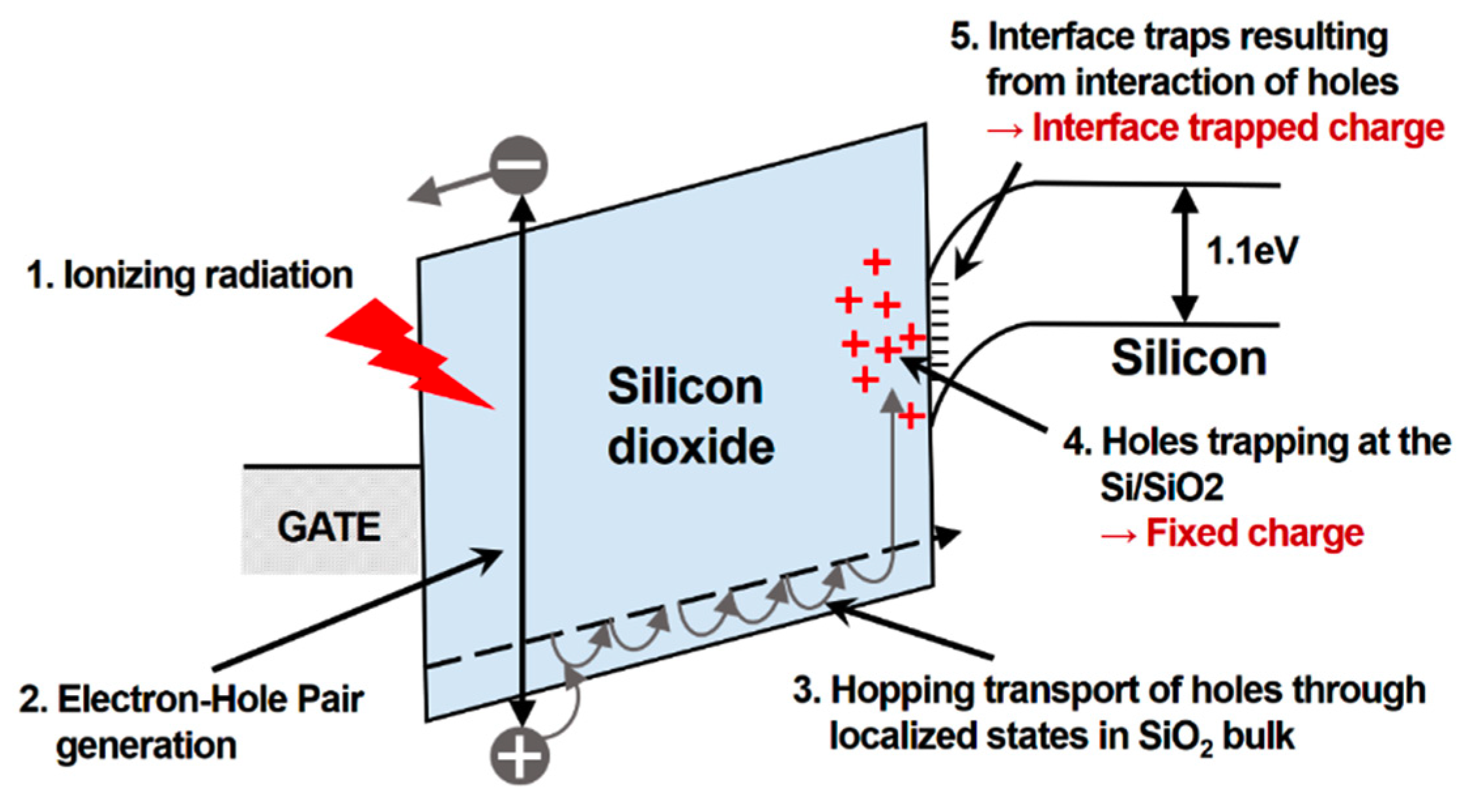
2.1. Cumulative Radiation-Induced Damage to MOSFETs
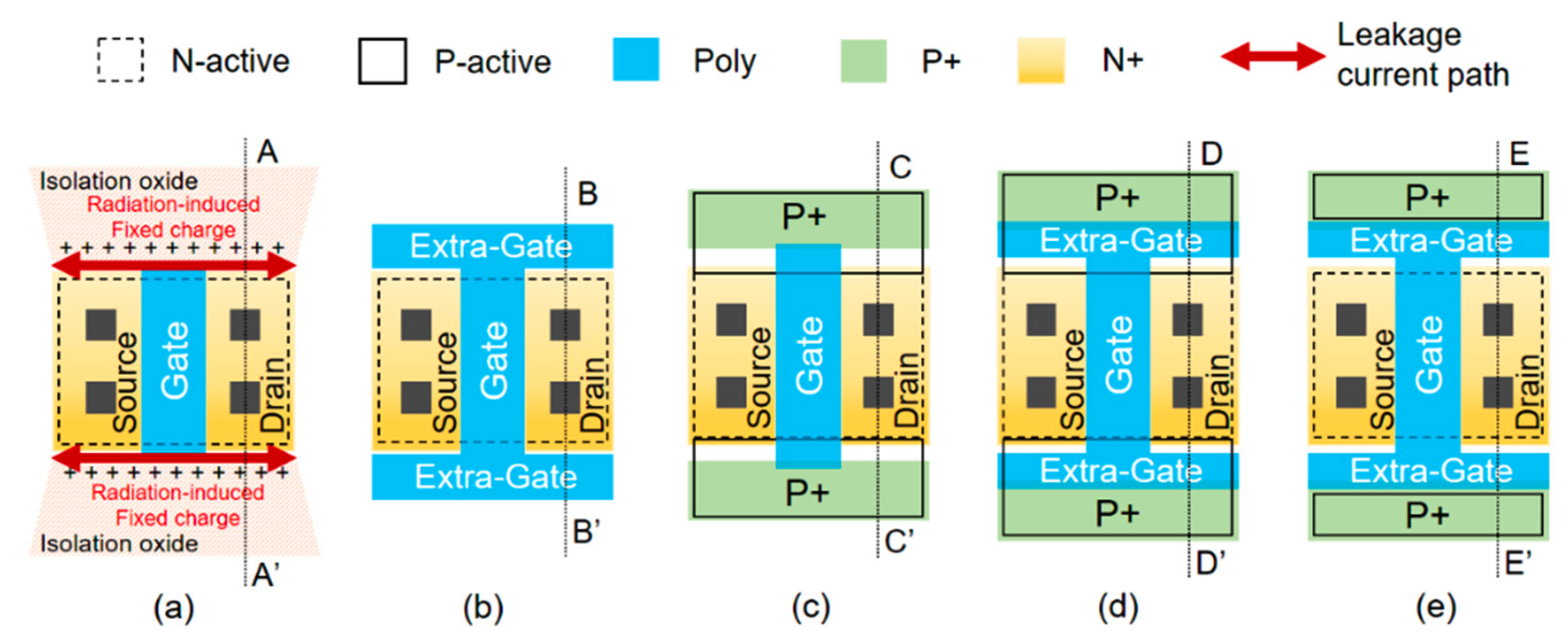
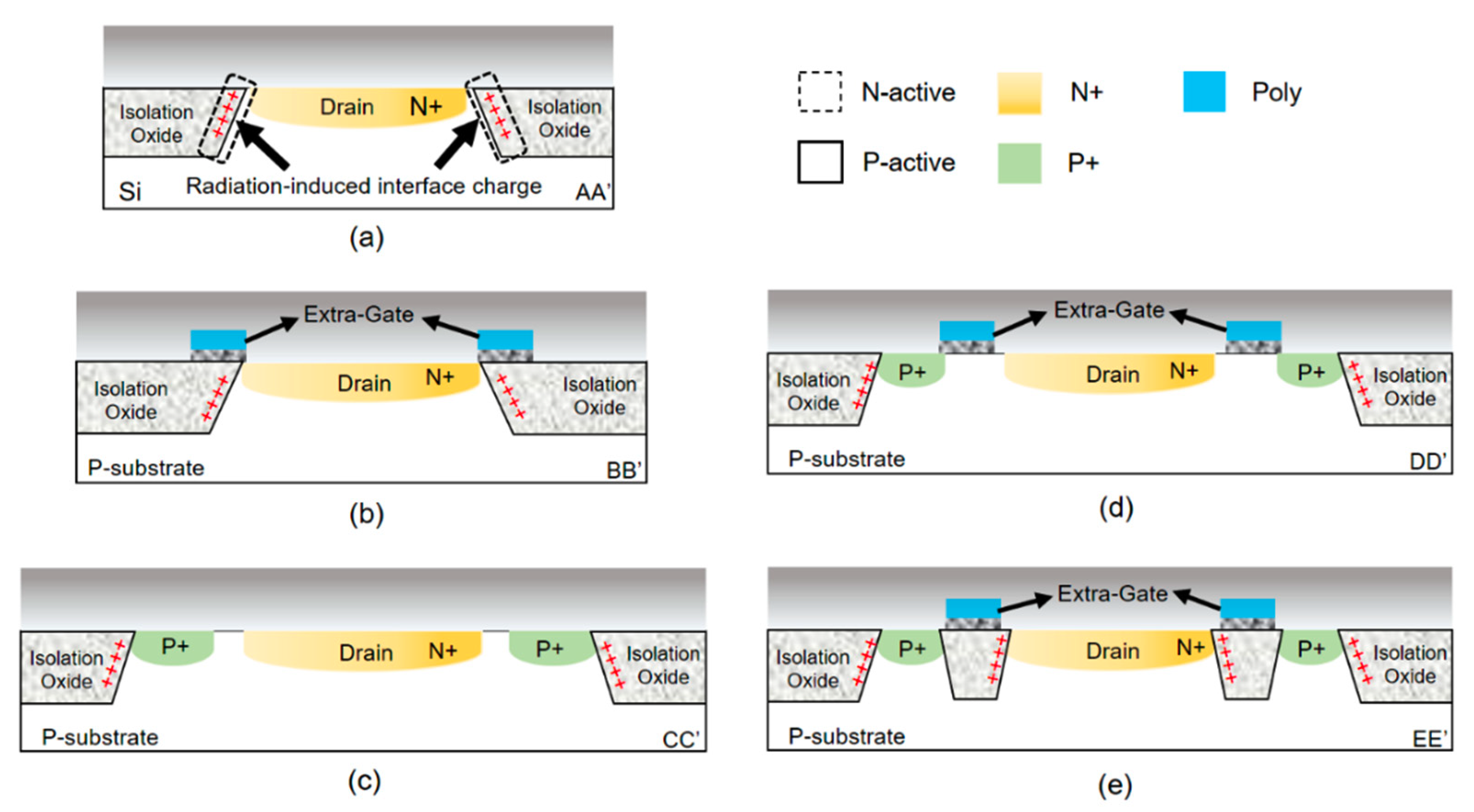
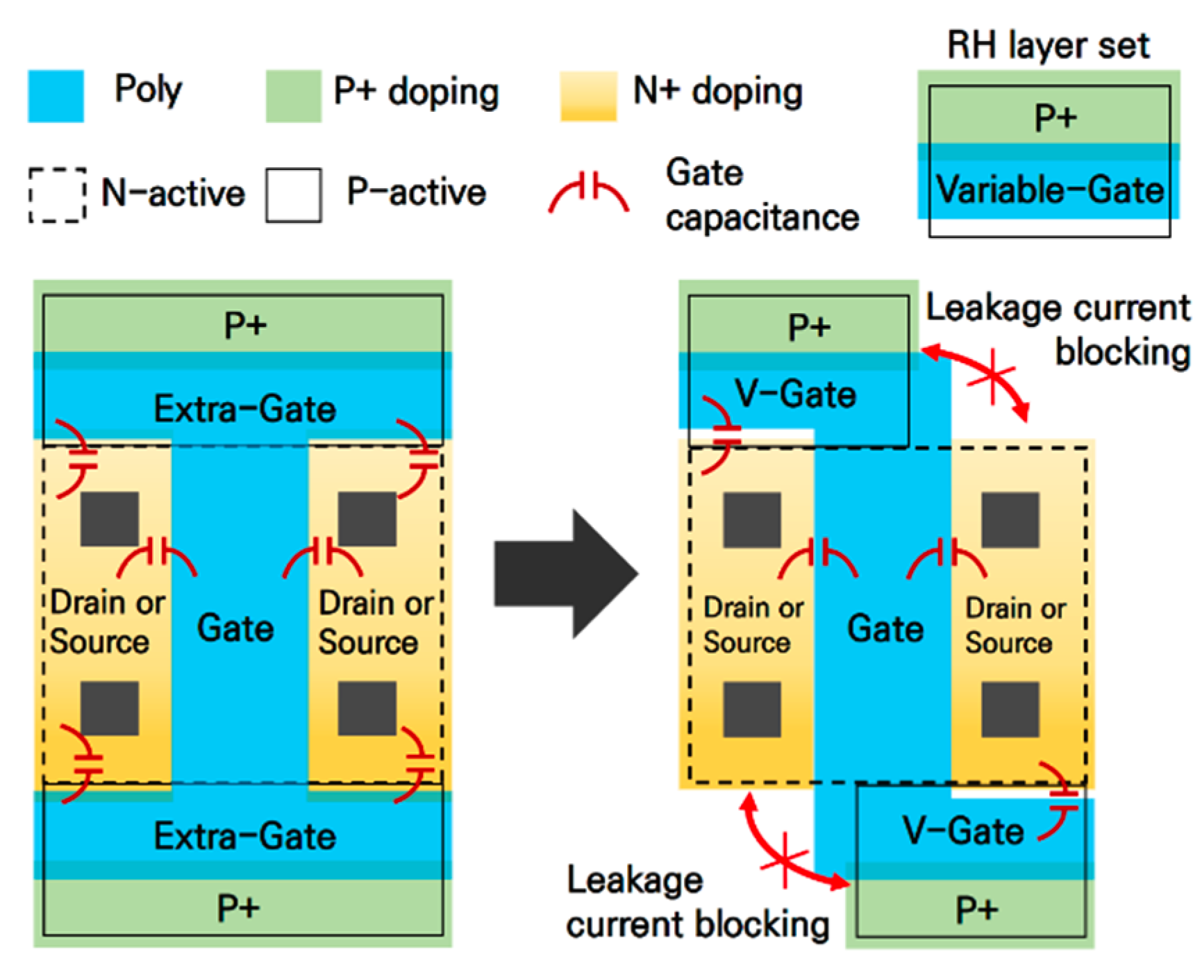
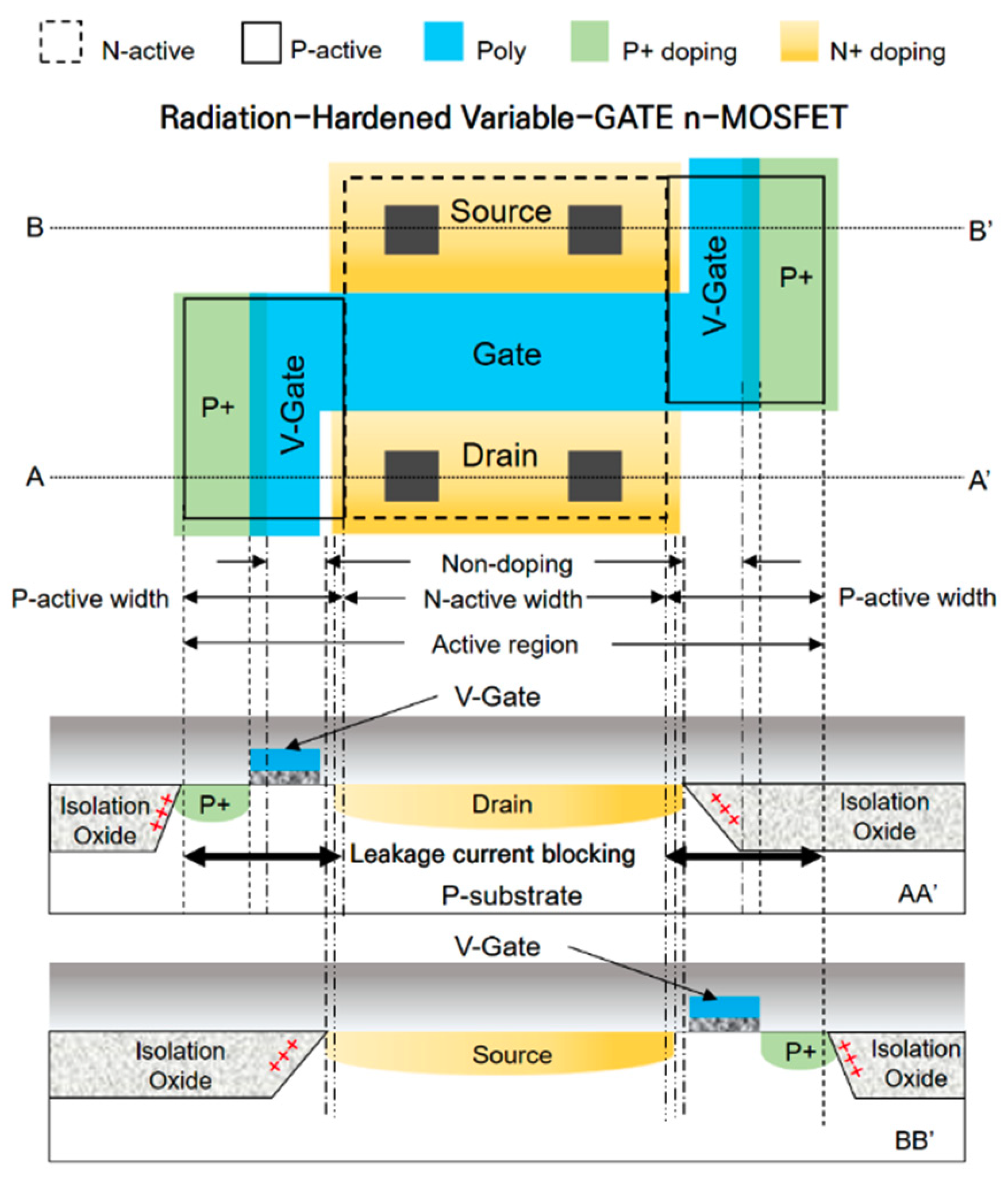
2.2. Structural Design of Radiation-Tolerant Layout
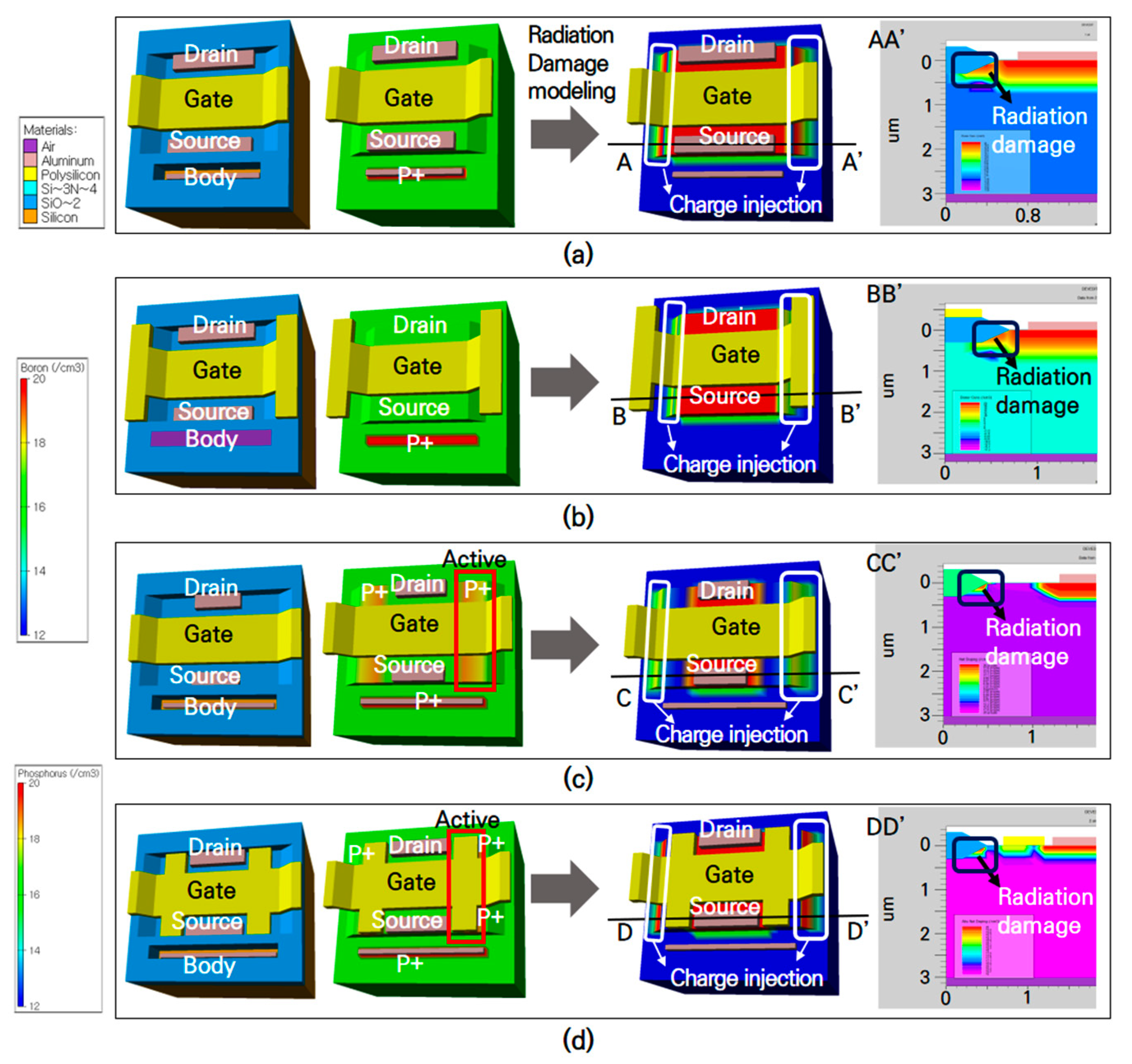
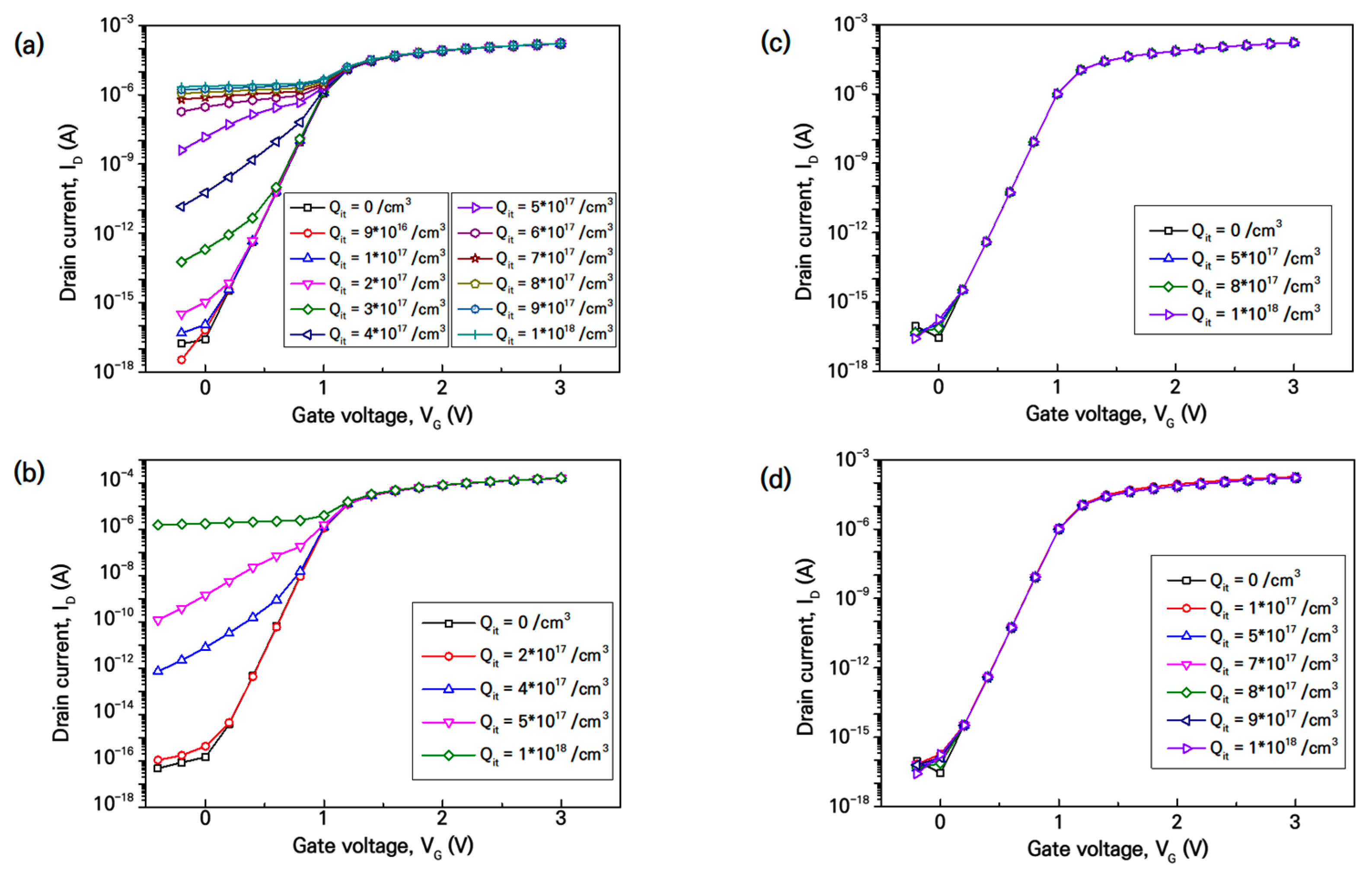
2.3. Using M&S to Assess Radiation Effect
2.4. Radiation Exposure Tests
3. Optimization of Radiation-Hardened n-MOSFET Design
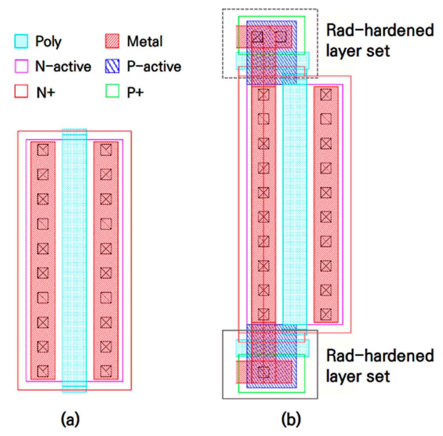
3.1. Design of Radiation-Hardened Variable-Gate n-MOSFET
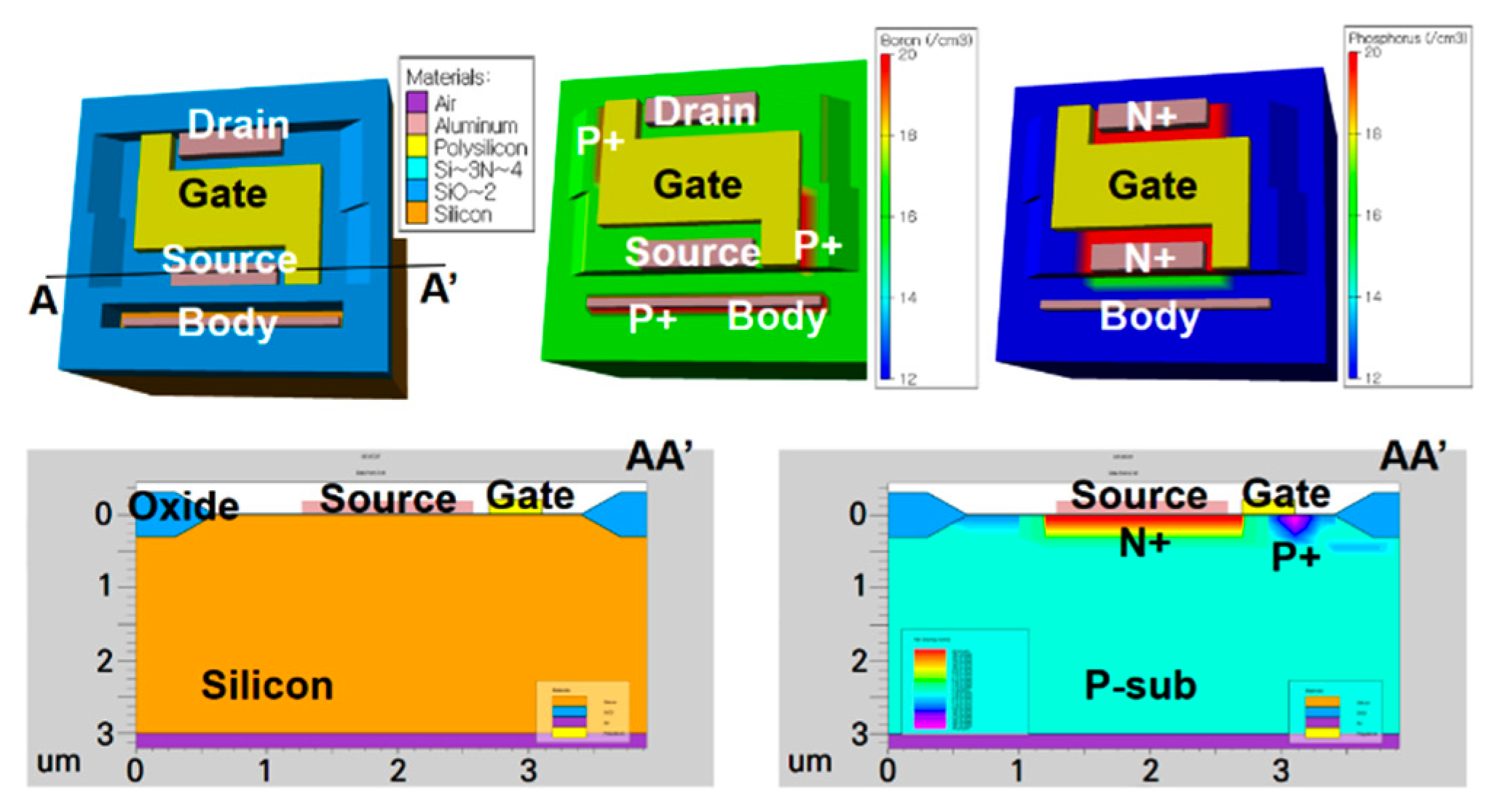
3.2. M&S of the Radiation Effect on RH Variable Gate n-MOSFET
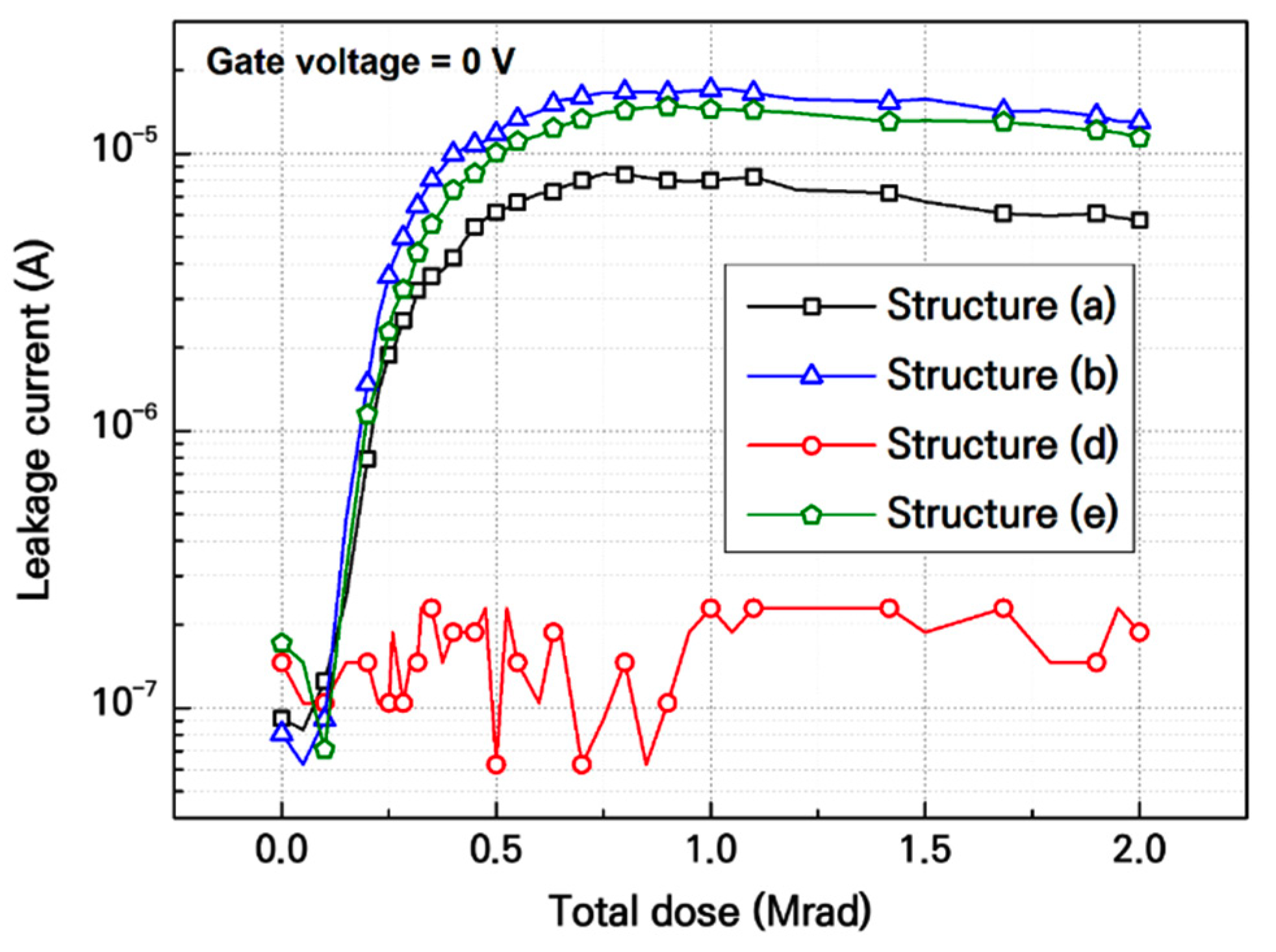
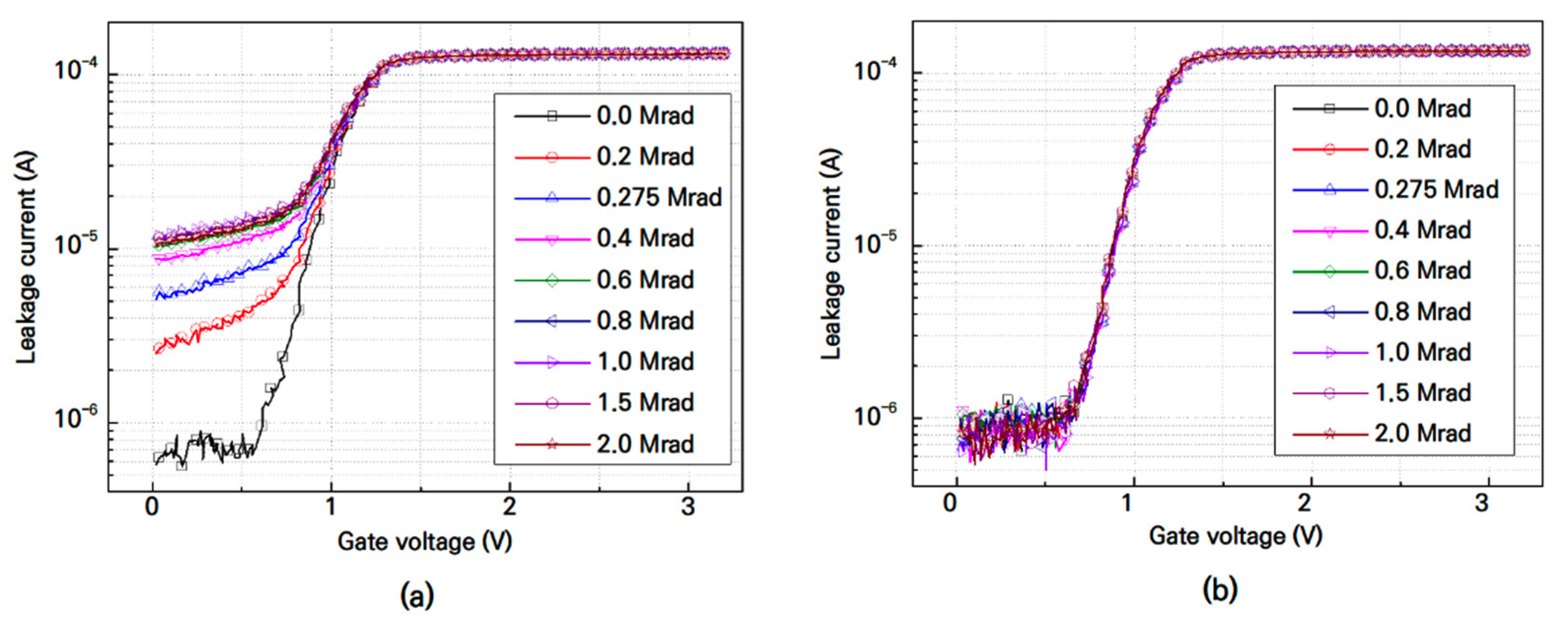
3.3. Radiation Exposure Tests and Results Analysis on RH Variable Gate n-MOSFET
4. Conclusions
Author Contributions
Funding
Conflicts of Interest
References
- Holmes-Siedle, A.; Adams, L. Handbook of Radiation Effects, 2nd ed.; Oxford Univ. Press: Oxford, UK, 2002. [Google Scholar]
- Oldham, T.R. Analysis of damage in MOS devices in several radiation environments. IEEE Trans. Nucl. Sci. 1984, 31, 1236–1241. [Google Scholar] [CrossRef]
- Edward, C.E. Radiation effects research in the 60’s. IEEE Trans. Nucl. Sci. 1994, 41, 2648–2659. [Google Scholar]
- Nidhin, T.S.; Bhattacharyya, A.; Behera, R.P.; Jayanthi, T.; Velusamy, K. Understanding radiation effects in SRAM-based field programmable gate arrays for implementing instrumentation and control systems of nuclear power plants. Nucl. Eng. Technol. 2017, 49, 1589–1599. [Google Scholar] [CrossRef]
- Srour, J.R.; McGarrity, J.M. Radiation Effects on Microelctronics in Space. Proc. IEEE 1988, 76, 1443–1469. [Google Scholar] [CrossRef]
- Sujatha, R.; Abdul, R.K.; Ravindra, M.; Damle, R. Study of effect fo gamma radiation on MOSFET for space applications. Indian J. Pure Appl. Phys. 2018, 56, 587–590. [Google Scholar]
- Messenger, G.C.; Ash, M.S. The Effects of Radiation on Electronic Systems; Springer Press: Van Nostrand Reinhold, NY, USA, 1992. [Google Scholar]
- Stephen, G.; van Nicolaas, V.; Steven, V.; Wesley, M. Integrated Circuit Design for Radiation Environments, 1st ed.; Wiley/John Wiley & Sons: Hoboken, NJ, USA, 2019. [Google Scholar]
- Lacoe, R.C.; Osborn, J.V.; Mayer, D.C.; Brown, S.; Koga, R. Application of hardness-by-design methodology to radiation-tolerant ASIC technologies. IEEE Trans. Nucl. Sci. 2000, 47, 2334–2341. [Google Scholar] [CrossRef]
- Deval, Y.; Lapuyade, H.; Rivet, F. Design of CMOS integrated circuits for radiation hardening and its application to space electronics. In Proceedings of the 2019 IEEE 13th International Conference on ASIC (ASICON), Chongqing, China, 29 October–1 November 2019. [Google Scholar]
- Schwank, J.R.; Shaneyfelt, M.R.; Draper, B.L.; Dodd, P.E. BUSFET-a radiation-hardened SOI transistor. IEEE Trans. Nucl. Sci. 1999, 46, 1809–1816. [Google Scholar] [CrossRef]
- Chen, L.; Gingrich, D.M. Study of N- Channel MOSFETs with an Enclosed-Gate Layout in a 0.18 um CMOS technology. IEEE Trans. Nucl. Sci. 2005, 52, 861–867. [Google Scholar] [CrossRef]
- Lee, M.S.; Lee, H.C. Dummy Gate- Assisted n-MOSFET Layout for a Radiation-Tolerant Integrated Circuit. IEEE Trans. Nucl. Sci. 2013, 60, 3084–3091. [Google Scholar] [CrossRef]
- Bezhenova, V.; Michalowska-Forsyth, A. Aspect ratio of radiation-hardened MOS transistors. Elektrotechnik Inf. 2018, 135, 61–68. [Google Scholar] [CrossRef]
- Luís Eduardo, S., Jr.; Odair Lellis, G.; Rafael, G.V.; da Antonio Carlos, C.T.; Saulo, F.; Salvador Pinillos, G. Minimizing the TID effects due to gamma rays by using diamond layout for MOSFETs. J. Mater. Sci. Mater. Electron. 2019, 30, 4339–4351. [Google Scholar]
- Chatzikyriakou, E.; Morgan, K.; Groot, C.H.K. Total ionizing dose hardened and mitigation strategies in deep submicrometer CMOS and beyond. IEEE Trans. Electron Devices 2018, 65, 808–819. [Google Scholar] [CrossRef]
- Louise, L.; Alexandre, Q.; Evelyne, D.; Fortunato, D. Effects of Ionizing Radiation in Semiconductor Device: Simulation with Geant4. Mardi Chercheurs. 2019. Available online: https://www.researchgate.net/publication/335882715_Effects_of_ionizing_radiation_in_semiconductor_devices_simulation_with_Geant4 (accessed on 21 February 2021).
- Giacomini, R.; Martino, J.A. Modeling Silicon on Insulator MOS Transistors with Nonrectangular-Gate Layouts. J. Electrochem. Soc. 2006, 153, G218–G222. [Google Scholar] [CrossRef]
- Barnaby, H.J. Total-Ionizing-Dose Effects in Modern CMOS Technologies. IEEE Trans. Nucl. Sci. 2006, 53, 3103–3120. [Google Scholar] [CrossRef]
- Fleetwood, D.M.; Winokur, P.S.; Reber, R.A.; Meisenheimer, T.L.; Schwank, J.R.; Shaneyfelt, M.R.; Riewe, L.C. Effects of oxide traps, interface traps, and ‘border traps’ on metal-oxide-semiconductor devices. J. Appl. Phys. 1993, 73, 5058–5074. [Google Scholar] [CrossRef]
- Oldham, T.R.; Mclean, F.B. Total Ionizing Dose Effects in MOS Oxides and Devices. IEEE Trans. Nucl. Sci. 2003, 50, 483–496. [Google Scholar] [CrossRef]
- Sang-hun, J.; Nam-ho, L.; Seong-ik, C. Analysis of Radiation Effects in CMOS 0.18um Process Unit Devices. Trans. Korean Inst. Electr. Eng. 2017, 66, 540–544. [Google Scholar]
- Benedetto, J.M.; Boesch, H.E., Jr.; McLean, F.B.; Mize, J.P. Hole removal in thin gate MOSFET’s by tunneling. IEEE Trans. Nucl. Sci. 1985, 32, 3916. [Google Scholar] [CrossRef]
- Saks, N.; Ancona, M.; Modolo, J. Generation of interface states by ionizing radiation in very thin MOS oxides. IEEE Trans. Nucl. Sci. 1986, 33, 1185–1190. [Google Scholar] [CrossRef]
- Lee, M.; Lee, N.; Kim, J.; Cho, S. New Radiation-Hardened Design of a CMOS Instrumentation Amplifier and its Tolerant Characteristic Analysis. Electronics 2020, 9, 388. [Google Scholar] [CrossRef]
- Esqueda, I.S.; Barnaby, H.J. Modeling the Non-Uniform Distribution of Radiation-Induced Interface Traps. IEEE Trans. Nucl. Sci. 2012, 59, 723–727. [Google Scholar] [CrossRef]
- Jacob Baker, R. CMOS: Circuit Design, Layout, and Simulation, 3rd ed.; John Wiley and Sons Ltd.: Hoboken, NJ, USA, 2010. [Google Scholar]
- Razavi, B. Design of Analog CMOS Integrated Circuits; FBW New Edition; McGraw-Hill: Boston, CA, USA, 2000. [Google Scholar]
- Ionizing Radiation (Total Dose) Test Procedure; MIL-STD-883H 1019.8; U.S. Department of Defense: Washington, DC, USA, 2010. Available online: http://everyspec.com/MIL-STD/MIL-STD-0800-0899/MIL-STD-883H_21092/ (accessed on 5 December 2020).
- Semenov, O.; Sarbishaei, H.; Axelrad, V.; Sachdev, M. The Impact of CMOS technology scaling on MOSFETs second breakdown: Evaluation of ESD robustness. Microelectron. Reliab. 2004, 44, 1817–1822. [Google Scholar]



| Category | Measurement Condition |
|---|---|
| Facility | Advanced Radiation Technology Institute |
| Radiation source | Cobalt-60 |
| Dose Rate | 0.5 Mrad/h(Si) |
| Total Dose | 2 Mrad(Si) |
| Test sample | pattern-specific n-MOSFETs (4-type) |
| Characteristic | Leakage current |
| Method | Real-time using 25 m cable |
| Input Bias | Supply voltage: 1.8 V, Gate voltage: 0 V–1.8 V |
| n-MOSFET Geometry | RH Variable Gate | |||
| Width/length (um/um) | Body thickness (um) | Gate oxide thickness (nm) | Isolation oxide thickness (um) | width/length (um/um) |
| 2/1 | 3 | 10 | 0.3 | 0.4/1.5 |
| n-MOSFET doping profile | ||||
| Region (type) | Doping density (/cm3) | Depth (nm) | Fuction | |
| Drain (n+) | 1*1020 | 80 | Gaussian, Error | |
| Source (n+) | 1*1020 | 80 | Gaussian, Error | |
| Body (p+) | 1*1016 | - | Constant | |
| Channel (n+) | 2*1017 | 35 | Gaussian, Step | |
| RH layer (p+) | 1*1019 | 80 | Gaussian, Error | |
Publisher’s Note: MDPI stays neutral with regard to jurisdictional claims in published maps and institutional affiliations. |
© 2021 by the authors. Licensee MDPI, Basel, Switzerland. This article is an open access article distributed under the terms and conditions of the Creative Commons Attribution (CC BY) license (https://creativecommons.org/licenses/by/4.0/).
Share and Cite
Lee, M.; Lee, N.; Kim, J.; Hwang, Y.; Cho, S. Modeling and Simulation-Based Layout Optimization for Tolerance to TID Effect on n-MOSFET. Electronics 2021, 10, 887. https://doi.org/10.3390/electronics10080887
Lee M, Lee N, Kim J, Hwang Y, Cho S. Modeling and Simulation-Based Layout Optimization for Tolerance to TID Effect on n-MOSFET. Electronics. 2021; 10(8):887. https://doi.org/10.3390/electronics10080887
Chicago/Turabian StyleLee, Minwoong, Namho Lee, Jongyeol Kim, Younggwan Hwang, and Seongik Cho. 2021. "Modeling and Simulation-Based Layout Optimization for Tolerance to TID Effect on n-MOSFET" Electronics 10, no. 8: 887. https://doi.org/10.3390/electronics10080887
APA StyleLee, M., Lee, N., Kim, J., Hwang, Y., & Cho, S. (2021). Modeling and Simulation-Based Layout Optimization for Tolerance to TID Effect on n-MOSFET. Electronics, 10(8), 887. https://doi.org/10.3390/electronics10080887


