Article

An FPGA-Based Four-Channel 128k-Point FFT Processor Suitable for Spaceborne SAR

Beijing Key Laboratory of Embedded Real-Time Information Processing Technology, Beijing Institute of Technology, Beijing 100081, China
*
Author to whom correspondence should be addressed.
Electronics 2021, 10(7), 816; https://doi.org/10.3390/electronics10070816
Submission received: 19 February 2021 / Revised: 25 March 2021 / Accepted: 27 March 2021 / Published: 30 March 2021
(This article belongs to the Section Circuit and Signal Processing)

Abstract

:
Spaceborne synthetic aperture radar (SAR) plays an important role in many fields of national defense and the national economy, and the Fast Fourier Transform (FFT) processor is an important part of the spaceborne real-time SAR imaging system. How to meet the increasing demand for ultra-large-scale data processing and to reduce the scale of the hardware platform while ensuring real-time processing is a major problem for real-time processing of on-orbit SAR. To solve this problem, in this study, we propose a 128k-point fixed-point FFT processor based on Field-Programmable Gate Array (FPGA) with a four-channel Single-path Delay Feedback (SDF) structure. First, we combine the radix-23 and mixed-radix algorithms to propose a four-channel processor structure, to achieve high efficiency hardware resources and high real-time performance. Secondly, we adopt the SDF structure combined with the radix-23 algorithm to achieve efficient use of storage resources. Third, we propose a word length adjustment strategy to ensure the accuracy of calculations. The experimental results show that the relative error between the processor and the MATLAB calculation result is maintained at about 10−4, which has good calculation accuracy.
Keywords:
spaceborne SAR; FFT; FPGA

1. Introduction

Spaceborne synthetic aperture radar is an important part of the field of space Earth observation. Because of its all-time and all-weather working capabilities, it has been widely used in many fields of national defense and the national economy, such as resource exploration and disaster monitoring [1,2,3,4,5].
Since the Seasat satellite of the National Aeronautics Administration (NASA) first demonstrated the ability of spaceborne synthetic aperture radar (SAR) to acquire high-resolution images of the world in 1978, many countries have begun to launch satellites carrying SAR payloads and to study spaceborne SAR imaging [6]. South Korea deployed its first SAR satellite KOMPSAT-5 in 2013, which has been used for all-weather and all-day observations of the Korean Peninsula [7]. Spain launched its first SAR satellite, PAZ, in 2018, mainly to meet the defense needs of the Spanish government [8]. The Canadian Missile Defense Agency developed a radar satellite constellation program [9] and launched three SAR satellites, including RCM 1, 2, and 3 in 2019, for detecting the Canadian mainland and the surrounding Arctic, Pacific, and Atlantic waters. China has developed a series of Yaogan SAR satellites, and recently launched Yaogan 33 in 2020, mainly for scientific experiments and disaster prevention and mitigation [10]. The United States proposed a Capella constellation plan consisting of 36 SAR satellites; Capella 1 was launched in 2018, and Capella 2, Capella 3 and Capella 4 will be launched in 2021 [11,12].
Most of the abovementioned tasks require real-time SAR data processing. The traditional processing method is to download the data from the satellite to the ground station for processing. However, under the observation modes of high resolution and large data granularity, the downloading time for the massive data diminishes the effects of improved ground processing capabilities. Obviously, real-time on-orbit processing to extract the information can effectively solve the above problems [13]. A high-performance on-board SAR real-time processing platform needs to be equipped with a processor that meets many constraints such as power consumption, performance, and capacity. At present, Central Processing Unit (CPU), Digital Signal Processing (DSP), Graphics Processing Unit (GPU), Application Specific Integrated Circuit (ASIC), and Field Programmable Gate Array (FPGA) processors have all demonstrated their superiority and shortcomings in real-time processing. The CPU processor undoubtedly has powerful processing capabilities and strong versatility, but its huge power consumption makes it unsuitable for the strong power constraints of on-orbit real-time processing [14]. DSPs have strong design flexibility and are easy to develop and maintain [15]; however, in the case of spaceborne SAR with massive data processing requirements, it is difficult for DSPs to provide a sufficient processing power/watt ratio (FLOPS/watt). The GPU processor has a high computing peak and high-speed memory interface, but once customized, the hardware resources cannot be changed. ASIC can provide sufficient processing capacity by virtue of its fully customized design, but a large-scale complex logic design requires more complete design verification and a longer development cycle. In recent years, FPGA has made significant progress in on-chip resource storage, computing resources, and software and hardware co-design. Therefore, FPGA can meet the needs of large throughput and strict real-time processing, and has the advantages of strong applicability, parallel computing, strong compatibility and flexible design. Due to these significant advantages, FPGA has gradually become the main technology used in real-time processing systems [16,17].
With the continuous improvement of SAR satellite observation capabilities and observation accuracy requirements of various countries, the observation angle of SAR satellites continues to increase, the observation range continues to expand, and the imaging resolution continues to improve [18,19]. These factors have led to increased granularity in data of SAR raw data and an increase in the data scale of a single SAR process. Therefore, the design for a SAR real-time processing system suitable for large-scale data is needed. Table 1 summarizes the models and resolutions of some SAR satellites. The Fast Fourier Transform (FFT) operation core is the most important operation module for SAR real-time processing, and its efficiency and scale greatly affect the processing speed and scale of the whole system [20]. Therefore, for data with high granularity, it is important to study the ultra-long point FFT processor that can adapt to the real-time processing requirements of on-orbit SAR.
In addition, the harsh space working environment places harsh requirements on the processing system in terms of volume, weight, and power consumption, and the choice of FFT processor data type has a significant impact on the scale of the hardware. Many researchers use single-precision floating-point numbers to design FFT processors. For example, Prasanna et al. [21] targeted the Virtex-5 FPGA device produced by Xilinx, and implemented a single-precision floating-point complex FFT processor in the form of fusion operations. This processor consumes less area and power consumption than a discrete implementation processor. Chen, J. et al. [22] proposed an FPGA-based configurable single-precision floating-point FFT processor, which reduced hardware costs by predicting the rotation direction and generated the rotation angle in real time to save memory resources. Prabhu, E. et al. [23] proposed an improved fusion single-precision floating-point product algorithm based on FPGA and an energy efficient butterfly unit model. The experimental results showed that the FFT processor using this model consumed less power than the previously proposed processor. Although these researchers proposed various ways to achieve savings in FPGA hardware resources and chip power consumption, they all use single-precision floating-point data types. Although floating-point FFT has the advantages of a simple design and convenient configuration, on the FPGA platform, floating-point numbers are much more complicated than fixed-point numbers in terms of representation methods and algorithms. Therefore, when the data bit width is the same or similar, floating-point numbers often occupy more hardware resources [22], and fixed-point numbers are more suitable for on-orbit processing systems with higher chip area constraints.
In order to further satisfy the constraints on processing area and power consumption of on-orbit processing, while taking into account the real-time performance of SAR data processing, the selection of the algorithm and structure used by the FFT processor is crucial. In terms of the FFT algorithm, Shaditalab, M. et al. [24] implemented a 512/1024 point parallel pipelined radix-2 FFT processor on FPGA, and Sun, Z. et al. [25] designed a 1024-point radix-4 FFT processor for SAR real-time processing on FPGA. The radix-2 and radix-4 algorithms have the advantages of simple unit and low computational complexity, and have better performance in applications where the number of FFT points is small; however, in real-time processing on-orbit scenarios that require extremely long FFT lengths, radix-2 and radix-4 algorithms require a high number of multiplier resources, and therefore have difficulty meeting the area constraints. In order to solve this problem, Chandu, Y. et al. [26] proposed a high-speed radix-8 FFT processor based on FPGA, which determined the occupation of FPGA logic resources by comparing radix-2, radix-4, and radix-8; they reported that the radix-8 algorithm had better area efficiency. Santhosh, L. et al. [27] implemented two FFT processors, radix-2 and radix-22 on FPGA, and proved that radix-2k series algorithms have a significantly higher utilization rate of logic resources than radix-k series algorithms. Tang, J. et al. [28] proposed an FFT processor based on a mixed-radix algorithm. The processor used the mixed-radix algorithm to achieve an eight-channel parallel structure, which greatly reduced the processing time. At the same time, the multi-channel parallel design was suitable for applications with large data throughput. In terms of processor structure, Yang, C. et al. [29] compared two typical pipelined FFT structures, Single-path Delay Commutator (SDC) and Single-path Delay Feedback (SDF), and verified that the SDF structure had more advantages in saving storage resources.
In this study, we propose an FPGA-based FFT processing design for an FFT processor that can support up to 128k point operations, which meets the needs of SAR imaging for ultra-long fixed FFT. We adopt a fixed-point number design scheme to reduce the overall FFT core’s requirements for chip memory and logic resources. In order to ensure the accuracy of fixed-point number operations, we adopt a word length adjustment strategy. In terms of algorithm and structure selection, we combine the radix-23 algorithm and the mixed-radix algorithm. The radix-23 algorithm of the SDF structure will significantly reduce the consumption of FFT check multiplier resources as compared with the radix-2 and radix-4 algorithms. The four-channel structure is implemented using a mixed-radix algorithm, which significantly reduces the FFT calculation time. Therefore, the FFT design scheme we propose reduces the scale of the hardware while ensuring the real-time performance of data processing. The main contributions of this study are summarized as follows:
  • A proposed FFT processor implemented on FPGA for on-orbit SAR processing is one that supports up to 128k fixed-point FFT operations, which further meets the needs of on-orbit SAR processing for ultra-long point FFT. The high-speed parallel 128k-point FFT processor is suitable for high-precision SAR real-time processing.
  • A radix-23 algorithm and a mixed-radix algorithm are combined with the advantages of low hardware resources and high real-time performance.
  • A word length adjustment strategy is proposed that can better ensure the accuracy of fixed-point calculations.
  • The designed processor is implemented on the Virtex-7 series FPGA device, and the calculation results are compared with the MATLAB double-precision floating point calculation results, showing that the relative error of the FPGA calculation results was maintained at about 10−4. We compared the designed processor with previous work, showing that the designed FFT processor requires fewer hardware resources.
The remainder of this paper is arranged as follows: in Section 2, we analyze the proportion of FFT in the chirp-scaling (CS) algorithm and introduce the principle and implementation details of the radix-23 and the mixed-radix algorithms; in Section 3, we introduce the hardware structure of the FFT processor, the radix-23 SDF pipelined structure, the fixed-point word length configuration scheme, and we propose a single-channel, four-channel FFT structure; the experiments and results are shown in Section 4; and finally, our conclusions are presented in Section 5.

2. Fast Fourier Transform (FFT) Operation Analysis and Principle Introduction

In a SAR imaging system, FFT processing undertakes most of the calculation work. Taking into consideration the desire to save hardware resources and reduce processing delay, the proposed FFT processor in this study, uses the radix-23 and mixed-radix algorithms.

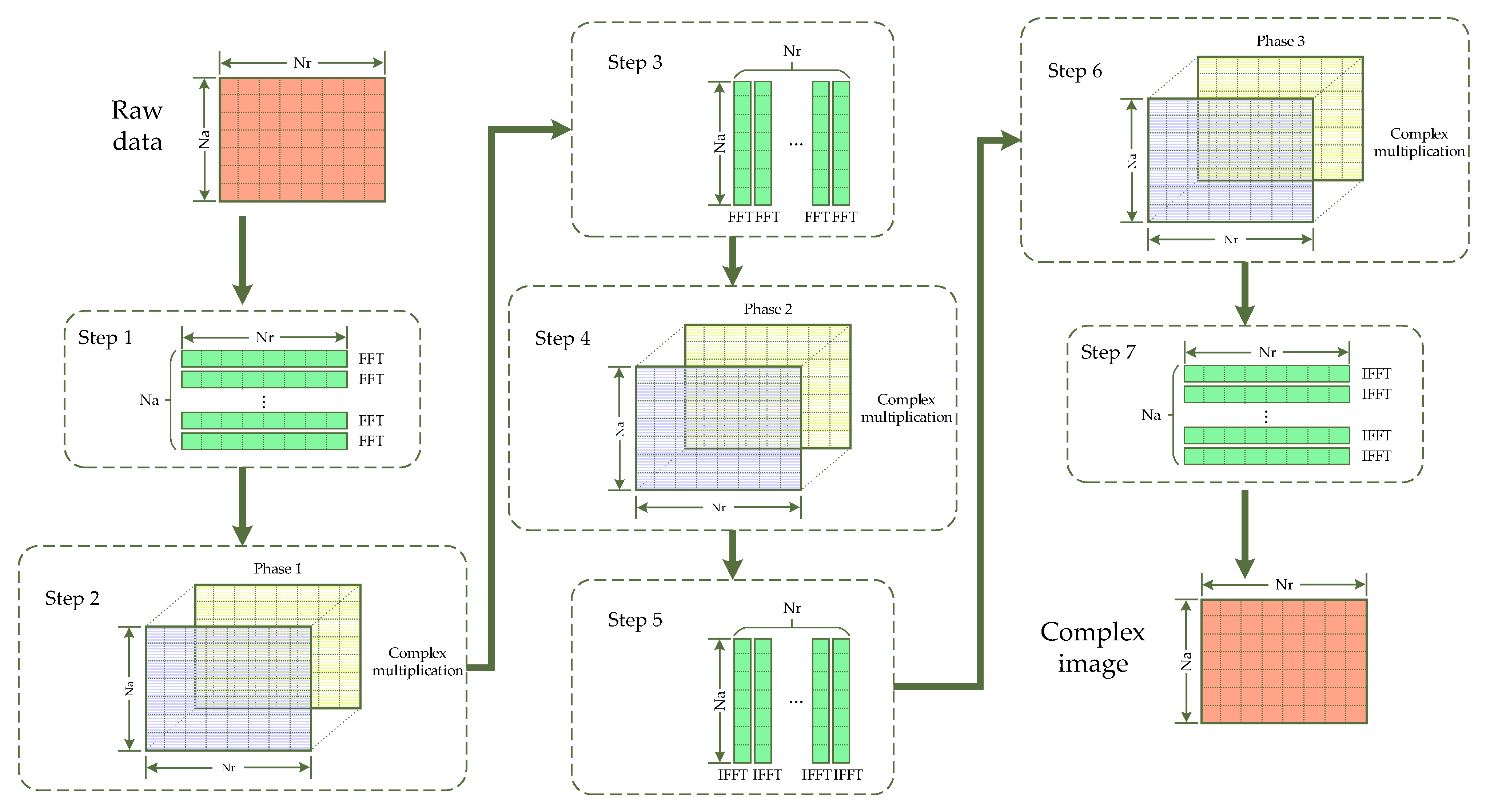
2.1. Operation Proportion Analysis of FFT in the Standard Chirp-Scaling (CS) Algorithm

In order to use synthetic aperture radar to accurately image targets, a variety of mature SAR imaging algorithms have been proposed. The chirp-scaling (CS) imaging algorithm proposed by Cumming et al. [30] in 1992, is often used as the core of an integrated algorithm, as well as the basis of other SAR imaging algorithms [20]. Therefore, it is important to study the proportion of the FFT operation in the standard CS imaging algorithm. The flowchart of the standard CS algorithm is shown in Figure 1.
In the algorithm flow, other operations, except FFT and inverse FFT (IFFT), are implemented by complex multiplication, so the number of real number additions and multiplications in the algorithm execution process can be used to measure the computational complexity of the entire algorithm and the complexity of hardware implementation. It is well known that data processed by a SAR system is a two-dimensional discrete signal. We assume that Na represents the number of sampling points of the original echo data in the azimuth direction, and Nr represents the number of sampling points of the echo data in the distance direction. Then, according to the processing flow of the CS algorithm, we can disassemble the CS algorithm into basic calculations, as shown in Figure 2.
Furthermore, we can calculate the real number of addition and multiplication computations required by FFT/IFFT and the whole algorithm. The comparison results of FFT/IFFT and phase factor complex multiplication operations are shown in Table 2 and Table 3. It should be noted that the basis of FFT/IFFT splitting here is the radix-2 algorithm.
The parameter η is used to represent the proportion of FFT/IFFT in the CS algorithm. It can be calculated using Equation (1).
η = [ 6 N r N a ( log 2 N r 1 ) + 6 N r N a ( log 2 N a 1 ) + 4 N r N a log 2 N r + 4 N r N a log 2 N a ] / [ 6 N r N a ( log 2 N r 1 ) + 6 N r N a ( log 2 N a 1 ) + 4 N r N a log 2 N r + 4 N r N a log 2 N a + 18 N r N a ] = 5 log 2 N r + 5 log 2 N a 6 5 log 2 N r + 5 log 2 N a + 3
We assume that the value of Na is also 128k and the value of Nr is 128k. According to Equation (1), η can be calculated to be approximately equal to 87%, which indicates that FFT is a key component of the SAR imaging system.

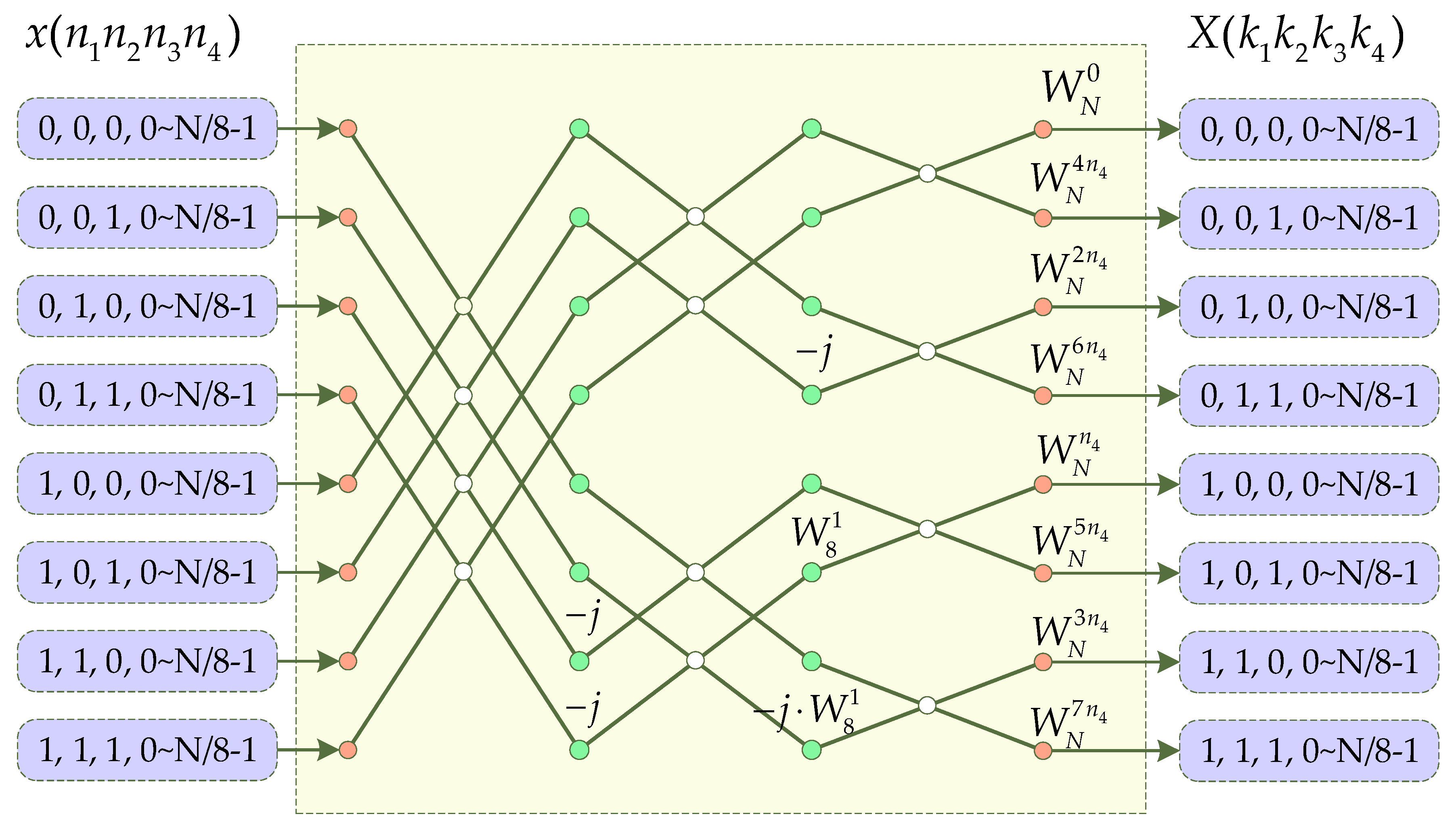
2.2. Introduction of the Radix-23 Algorithm

In this study, in order to avoid the problem that radix-2, radix-4, and other algorithms occupy too many logic resources in the scenario of ultra-long points, the radix-23 algorithm is adopted. The radix-23 algorithm can be derived from the N-point discrete Fourier transform (DFT) definition using Equation (2) as follows:
X ( k ) = n = 0 N 1 x ( n ) W N n k ,   0 k N
When N is an integral multiple of 8, n and k can be decomposed in the following ways in Equation (3). Since the processor proposed in this study is oriented to sequential data in the time domain, it uses the sampling method in the frequency domain. If the bit reverse data need to be processed in some scenes, the decomposition methods of n and k need to be exchanged using Equation (3) as follows:
{ n = N 2 n 1 + N 4 n 2 + N 8 n 3 + n 4 n 1 = 0 , 1   n 2 = 0 , 1   n 3 = 0 , 1   n 4 = 0 , 1 , , N 8 1 k = k 1 + 2 k 2 + 4 k 3 + 8 k 4 k 1 = 0 , 1   k 2 = 0 , 1   k 3 = 0 , 1   k 4 = 0 , 1 , , N 8 1
Substituting this decomposition method into the definition of Equation (2) results in the following:
X ( k ) =   n 1 = 0 1 n 2 = 0 1 n 3 = 0 1 n 4 = 0 N 8 1 x ( n ) W N ( k 1 + 2 k 2 + 4 k 3 + 8 k 4 ) · ( N 2 n 1 + N 4 n 2 + N 8 n 3 + n 4 ) =   n 1 = 0 1 n 2 = 0 1 n 3 = 0 1 n 4 = 0 N 8 1 x ( n ) W N N 2 k 1 n 1 + N 4 k 1 n 2 + N 8 k 1 n 3 + k 1 n 4 + N 2 k 2 n 2 + N 4 k 2 n 3 + 2 k 2 n 4 + N 2 k 3 n 3 + 4 k 3 n 4 + 8 k 4 n 4 =   n 1 = 0 1 n 2 = 0 1 n 3 = 0 1 n 4 = 0 N 8 1 x ( n ) · ( 1 ) k 1 n 1 · ( j ) k 1 n 2 · ( e j π 4 ) k 1 n 3 · ( 1 ) k 2 n 2 · ( j ) k 2 n 3 · ( 1 ) k 3 n 3 · W N n 4 ( k 1 + 2 k 2 + 4 k 3 ) · W N 8 k 4 n 4
In the end of Equation (4), the term, ( 1 ) n 1 k 1 , ( 1 ) n 2 k 2 , ( 1 ) n 3 k 3 , can be realized by a structure composed of basic butterfly elements. Take ( 1 ) n 1 k 1 as an example; we use “expression (1)” to represent the other parts of Equation (4) except ( 1 ) n 1 k 1 . After that, we expand the term ( 1 ) n 1 k 1 , and the result is shown in Equation (5). Obviously, this can be realized by a radix-2 butterfly element.
{ X ( k 1 = 0 ) = n 1 = 0 1 n 2 = 0 1 n 3 = 0 1 n 4 = 0 N 8 1 [ x ( n 1 = 0 ) + x ( n 1 = 1 ) ] · expression ( 1 ) X ( k 1 = 1 ) = n 1 = 0 1 n 2 = 0 1 n 3 = 0 1 n 4 = 0 N 8 1 [ x ( n 1 = 0 ) x ( n 1 = 1 ) ] · expression ( 1 )
In the same way, ( 1 ) n 2 k 2 and ( 1 ) n 3 k 3 can also be realized by this method. Finally, we can use the structure in Figure 3 to realize these three terms. In Figure 3, the input data x(n) is divided into eight groups according to the different values of n 1 , n 2 and n 3 , and the range of n 4 in each group is 0 N 8 1 , which is not shown in the figure. We can find that the index value of each column is gradually transformed from n to k, which is a process from the time domain to the frequency domain.
We further add terms ( j ) k 1 n 2 , ( j ) k 2 n 3 and ( e j π 4 ) k 1 n 3 to the structure in Figure 3. Take ( j ) k 1 n 2 as an example; we can find that data groups in the second column, seventh row and eighth row have k 1 = 1 and n 2 = 1 , so we need to multiply these two sets of data by “−j”. In the same way, at the end of this structure, term W N n 4 ( k 1 + 2 k 2 + 4 k 3 ) needs to be multiplied by the result of each group of data. In summary, Figure 4 shows the implementation structure diagram of the radix-23 algorithm.
There are different hardware implementation schemes for the multiplication of each weight and signal in the flowchart. The realization process of the “−j” term multiplication is divided into two parts, i.e., exchange the position of the real part and the imaginary part of the data in the memory, and use the adder to negate the imaginary part after the position exchange; the term W 8 1 is a constant factor, and the multiplication of the constant factor and the data can be realized by a set of specific shifters and adders; the other terms are non-constant factors, and the multiplication with the data must first generate the corresponding sine and cosine values through the CORDIC kernel, and then use the multiplier on the FPGA to complete the calculation. Among them, the realization scheme of the multiplication of “−j” and a constant factor is the reason why the radix-23 algorithm saves multiplier resources.
When designing processors of the same length under the same FFT structure, if different algorithms are used to implement them, the theoretical consumption values of hardware resources for each algorithm are different. Single-path delay feedback (SDF) circuit structure to implement a pipelined FFT structure has the advantages of less memory requirement and high data throughput. The SDF structure is introduced in detail in the following sections. Table 4 lists the occupancy of the multiplier, memory unit, and butterfly unit by applying common radix-2, radix-4, and radix-23 algorithms, mentioned in this paper, when using the SDF structure to implement N-point FFT. The statistics of the multiplier occupancy in Table 4 refers to the number of multipliers that, theoretically, are required in the realization of non-constant factor multiplication. The statistics of the memory unit occupancy refers to the data depth that the memory Block RAM (BRAM) needs to provide during the implementation process, so this value does not represent the data width. The occupation of the butterfly unit refers to the number of basic units that need to be placed in the processor. R2 represents the radix-2 butterfly unit, and R4 represents the radix-4 butterfly unit. Figure 5 shows the structure diagram of the radix-4 algorithm. It can be seen from Table 4 that the most significant feature of the radix-23 algorithm is to save the use of multiplier resources. The three algorithms occupy the same memory resources, which is the result of the use of the SDF structure. The radix-23 and radix-2 algorithms are consistent in the occupancy of the butterfly unit; due to the complex implementation structure of the radix-4 butterfly unit, even if the occupancy is half of the radix-2 unit, it still takes up the most hardware resources. Specifically, the implementation of a single radix-4 unit requires 24 adders, while the realization of a single radix-2 unit requires only four adders. We can see from Figure 5 that the radix-4 structure includes four 4-input 1-output complex adders, and each 4-input 1-output complex adder needs six adders to implement.
When we assume that N is 128k, the radix-23 algorithm can save 68.6% and 37.3% of the multiplier resources as compared with the radix-2 and radix-4 algorithms, respectively. When the number of FFT points is higher, the saving of the multiplier is more obvious, and the radix-23 algorithm inherits the simple butterfly unit in the radix-2 algorithm. In summary, the advantages of the radix-23 algorithm include lower algorithm structure complexity, easy implementation, saving of hardware resources, etc., as compared with the radix-2 and radix-4 algorithms, and it is more suitable for applications with ultra-long points.

2.3. Introduction of Mixed-Radix Algorithm

Considering the high real-time performance of the processor, we adopted a mixed-radix algorithm to achieve a four-channel FFT structure, which could theoretically shorten the processing time by about four times. The mixed-radix algorithm refers to the decomposition of DFT according to at least two decomposition methods, and the time domain index and frequency domain index in Equation (2) are decomposed as follows:
{ n = L · m + l m = 0 , 1 , , M 1 ; l = 0 , 1 , , L 1 k = i + M · j i = 0 , 1 , , M 1 ; j = 0 , 1 , , L 1 N = L · M M = 2 k
In Equation (6), L is regarded as the number of channels, and M is regarded as the number of FFT points calculated in a single channel. When k is an integral multiple of 3, the radix-23 algorithm can be used. Substituting Equation (6) into Equation (3) results in the following equation:
X ( i + M · j ) =   m = 0 M 1 l = 0 L 1 x ( L · m + l ) W N ( L · m + l ) · ( i + M · j ) =   m = 0 M 1 l = 0 L 1 x ( L · m + l ) W N i l · W M m i · W L l j =   l = 0 L 1 X l ( i ) W N i l · W L l j
In Equation (7), there are the following results:
X l ( i ) = m = 0 M 1 x ( L · m + l ) W M m i
From Equations (7) and (8), the mixed-radix algorithm can be summarized as the process of decomposing an N-point FFT into a L × M-point FFT. The number of FFT processor points, designed in this study, is 128k, and the decomposition method of 4 × 32k is adopted. Where M = 32k, which is realized by the five-stage radix-23 algorithm, L = 4, which can be implemented by the radix-4 butterfly unit. Substituting numbers into Equations (7) and (8), the following results can be obtained:
X ( i + 32 k · j ) = l = 0 3 [ X l ( i ) · W 128 k i l ] · W 4 l i
X l ( i ) = m = 0 32 k 1 x ( 4 · m + l ) W 32 k m i
In Equation (9), we can regard X l ( i ) · W 128 k i l as the input data of the radix-4 algorithm. Since there are four values for l, we first use the FFT processors with a length of 32k points to calculate X l ( i ) in Equation (9), and then multiply X l ( i ) by W 128 k i l . Finally, we use the radix-4 algorithm to process this result.
However, in order to simplify the design, in this study, we use the radix-22 algorithm to achieve the same function as the radix-4 algorithm, that is, the radix-22 algorithm and the radix-4 algorithm have exactly the same input and output values, and the principle of the radix-22 algorithm is similar to that of the radix-23 algorithm. The radix-22 algorithm structure diagram is shown in Figure 6. It is worth noting that, in order to emphasize the function of the four-channel and mixed-radix algorithm of the FFT processor designed in this article, the “radix-4 algorithm” instead of the “radix-22 algorithm” is used afterwards.
It can be clearly seen from Figure 7 that the four-channel FFT parallel structure can save three-quarters of the time as compared with the single-channel FFT algorithm. The radix-4 structure can be implemented through combinational logic circuits without introducing new processing delays. Therefore, the four-channel design can make full use of hardware resources, increase the number of FFT calculation points, and greatly reduce the FFT calculation time. However, an increase in the number of channels means that the processing bandwidth is doubled; therefore, the number of channels is limited by the processing bandwidth and data transmission bandwidth of the FPGA.

3. Hardware Implementation of the FFT Processor

On the basis of the algorithm proposed in Section 2, in this section, we propose the hardware implementation of the FFT processor, including implementation of the radix-23 algorithm under an SDF structure, a strategy of fixed-point FFT word length adjustment, single-channel FFT processor structure, and four-channel FFT processor structure. The implementation of the single-channel FFT processor only uses the radix-23 algorithm proposed in Section 2.2, and the implementation of the four-channel FFT processor refers to the structure of the single-channel FFT processor and uses the mixed-radix algorithm proposed in Section 2.3. The specific implementation schemes of each part are introduced in this section.

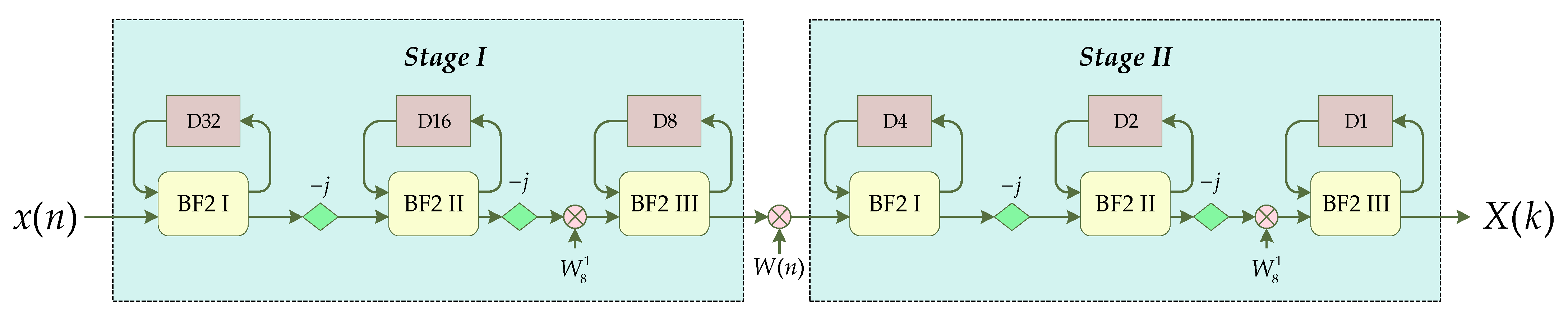
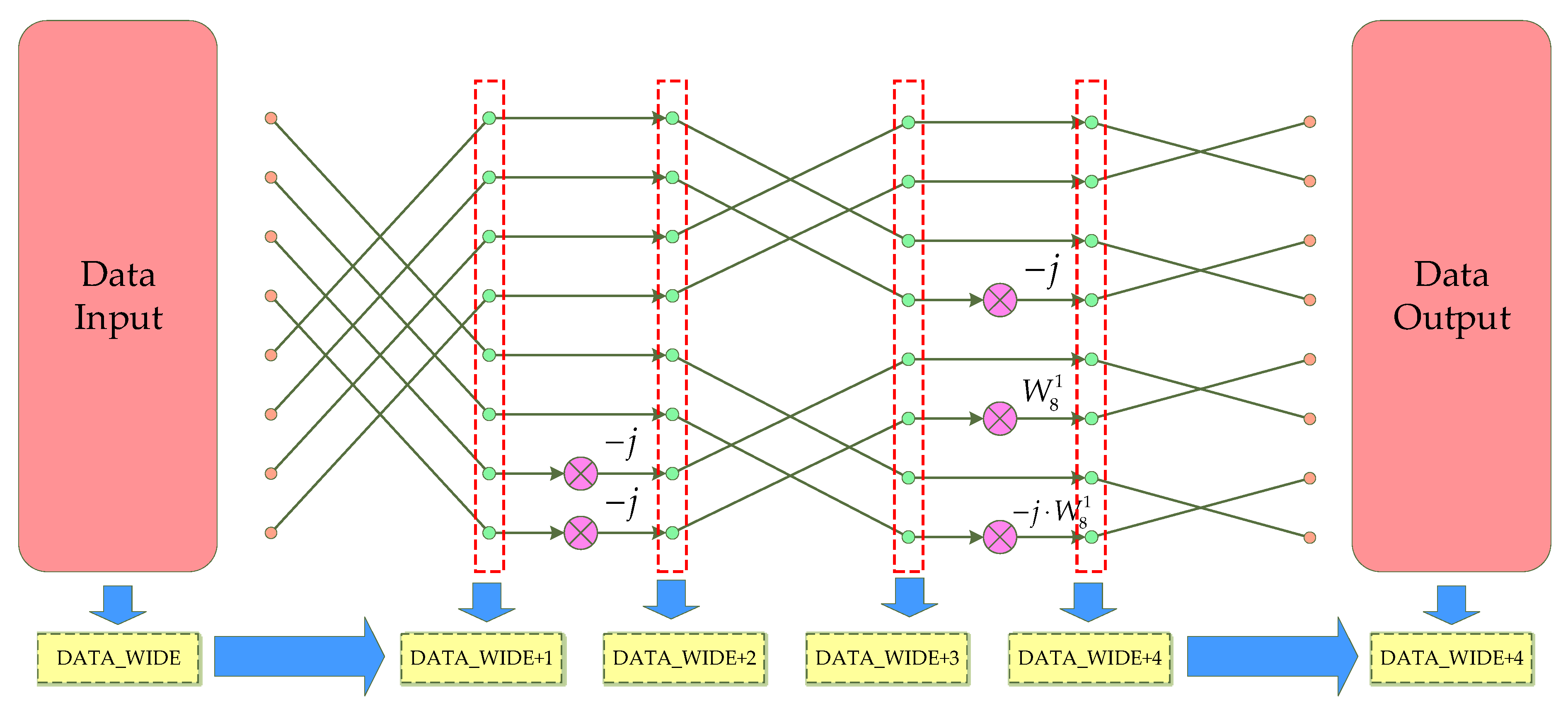
3.1. Implementation of the Radix-23 Algorithm under Single-Path Delay Feedback (SDF) Structure

Using a Single-path Delay Feedback (SDF) circuit structure to implement a pipelined FFT has the advantages of less memory requirement, fewer logic resources, and fast operation speed [5]. Combining the radix-23 algorithm with the SDF structure results in the radix-23 SDF structure diagram, as shown in Figure 8 (64-point FFT is taken as an example in Figure 8). In Figure 8, D represents the delay unit, which is used to buffer the data input first to wait for the data input later. This unit is implemented using (Block RAM) BRAM on the FPGA. Taking D32 as an example, it means that the delay unit set needs to buffer 32 points of data, that is, the data depth of the BRAM is 32. Because the data bit width will change during the calculation process, each D unit is set independently. BF in the figure represents the radix-2 butterfly operation unit, and BFI, BFII, and BFIII distinguish the different positions of the butterfly unit. The unit corresponds to the delay unit, one by one. It has dual inputs and dual outputs ports; a set of inputs and outputs cooperate with the delay unit to read and write to the buffer area. In addition, one input port is used to receive the data input by the serial pipeline, and an output port is used to output the data calculated by the butterfly unit and used as the input of the next butterfly unit. The stage in the figure represents a complete radix-23 algorithm structure (not including non-constant factor multiplication). A stage contains three D units, three BF units, two “−j” multipliers, and a W 8 1 constant factor multiplier. The 64-point FFT is divided into two operational stages in the radix-23 SDF structure. The output data of the first operator needs to be multiplied by non-constant factors as the input of the second operational stage.
The data processing involves the following. The first 32 points of the 64-point data flow into this structure, and the data are cached in D32 corresponding to radix-2 butterfly unit Stage 1 (BF2I). When the last 32 points of the data flow in each point are received, the butterfly operation is directly performed with the data of the corresponding address in D32. After the calculation is completed, the result of the addition operation in the butterfly unit is sent to the next stage, namely BF2II, and the result of the subtraction operation in the butterfly unit is fed back to the buffer area of this stage, namely D32, to cover the corresponding data. When the last 32 points of data are all received, the content saved in D32 is the result of the first-stage butterfly operation subtraction. At this time, the input 0 sequence is used to drive the first stage, and the data are sent to the next stage one by one. In the subsequent stages, the method of data flow is the same. The only difference is that the size of the memory unit at each stage is different, which corresponds to a gradual decrease in the data interval involved in the butterfly operation in the FFT algorithm. The operation of each BF2 in the pipelined processing process is shown in Figure 9. As shown in the figure, since the data that arrive first during a butterfly operation need to wait for the data that arrive later, there is an idle period in each stage of the BF2 when the processor starts working. However, when the processor continuously processes multiple sets of 64-point data, it will only be idle when the first set of data is processed, and it needs to be driven by a zero sequence after the last set of data is input.

3.2. Strategy of Fixed-Point FFT Word Length Adjustment

It is well known that the width of a single-precision floating-point number is 32 bits, including 1 sign bit, 8 exponent bits, and 23 decimal bits. The data type used in this study is a 32-bit fixed-point number, including 1 sign bit and 31 decimal bits. Comparing the two data types, it can be seen that the floating-point numbers can represent a wide range of data because of their exponent bits, but they are not as accurate as the 32-bit fixed-point number. For example, when representing a number near 0.5, the floating-point number can be accurate to approximately 10−7, while the 32-bit fixed-point number can be accurate to approximately 4 × 10⁻¹⁰. In fact, if the representation range of the data is known, we can specify the position of the decimal point in the fixed-point number and place the representation range of the fixed-point number near the data range, that is, artificially realize the exponent in the floating-point number. Combined with the analysis in Section 1, a 32-bit fixed-point number has the advantages of higher data accuracy, simpler implementation circuits, and shorter processing delays than a single-precision floating-point number. However, the representation range of a fixed-point number is limited, and overflow is prone to occur in the process of addition and multiplication. The word length must be adjusted after each operation to prevent overflow.
The bit width before the data flows into the operation stage is assumed to be DATA_WIDE, which indicates the bit width of the real and imaginary parts of the data. When the data pass through the radix-2 butterfly unit, they participate in addition and subtraction operations, and the data bit width is extended by one bit to ensure that the calculation result does not overflow. When data are multiplied with a constant factor and a non-constant factor, since the modulus of the factor is one, the change ratio of the real part and the imaginary part of the data is up to 2 times, so the data bit width only needs to be extended by 1 bit and it can ensure that the calculation does not overflow. A single-channel 32k-point FFT requires a total of five radix-23 units to be cascaded. Figure 10 shows the data word length adjustment strategy of a one-stage radix-23 butterfly unit.

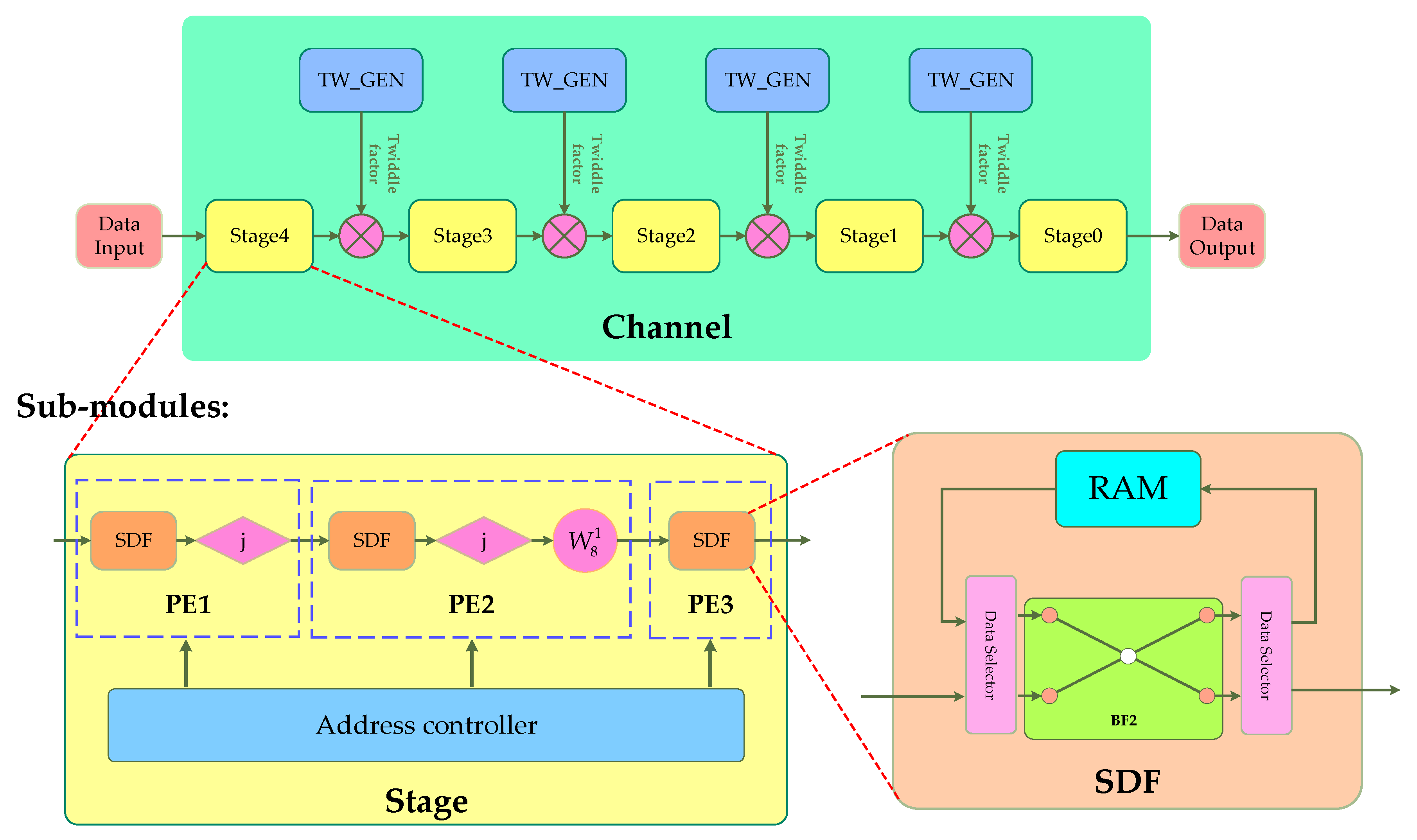
3.3. Single Channel FFT Processor Structure

According to the radix-23 algorithm scheme, a single-channel 32k-point FFT processor contains five radix-23 operation stages, that is, 32k = 85. The five operating stages are serially connected through four non-constant factor multipliers. The output data of the previous stage is used as the data input of the next stage through the non-constant factor multiplier, thus, forming a channel FFT structure, as shown in Figure 11. The stage unit in the figure is the same as the stage structure in Figure 8, but the size of the D unit is different; the TW_GEN unit generates the required twiddle factors in real time and provides them to the non-constant factor multiplier. It can be seen from the figure that each stage contains three processing units (PE1–PE3) and an address controller; each processing unit contains an SDF structure. In addition, PE1 contains a −j term multiplier, and PE2 contains −j and W 8 1 multiplier; each SDF structure contains a RAM unit (D unit in Figure 8), a radix-2 butterfly unit (BF2) and two data selectors.
The functions and implementation methods of each module are as follows:
The radix-2 butterfly unit (BF2) realizes a complex butterfly operation, which contains logic circuits for the addition and subtraction of complex numbers.
The data selector is used to determine the inflow and outflow direction of data, which contain address control logic to control RAM and work with the BF2.
The SDF module implements a pipeline to receive input data, and a pipeline to output the data after the radix-2 butterfly calculation. The SDF module contains a piece of RAM, which can be easily implemented by calling the IP core Block Memory Generator.
The processing unit modules (PE1, PE2, and PE3) are used to rotate the data in a specific direction after the SDF structure, that is, to multiply the factors −j and W 8 1 .
The address controller is used to provide the three SDF structures with the address values of the current read and write operations on the RAM in each clock cycle, and indicate the current operation of the SDF structure on the RAM (cache the newly input data or cache the BF2 settlement result). The logic of the address controller is completely based on the sequence value of the current incoming time domain data, and therefore it can also be considered a data flow controller.
The function of the operation–stage module (stage) is to complete the processing of data at an operation stage and output the results and their corresponding addresses in a pipeline.
The TW_GEN module is used to generate the twiddle multiplication factor required for each clock to be used as the input of the non-constant factor multiplier. In this module, the CORDIC IP core in the FPGA needs to be called. The IP core is used to generate the sin(x) value and the cos(x) value when the input is x; the value of x can be summarized as Equation (11) using Equation (4) and Figure 4. We name the TW_GEN connected after Stage 4 as TW_GEN4, and so on. For Equation (11), the numerical change rule of each parameter in each TW_GEN module is shown in Table 5. Except for N, which is a fixed value, other values change in each clock cycle with the value in Table 5 using Equation (11) as follows:
x = 2 π N · n 4 · ( k 1 + 2 k 2 + k 3 )

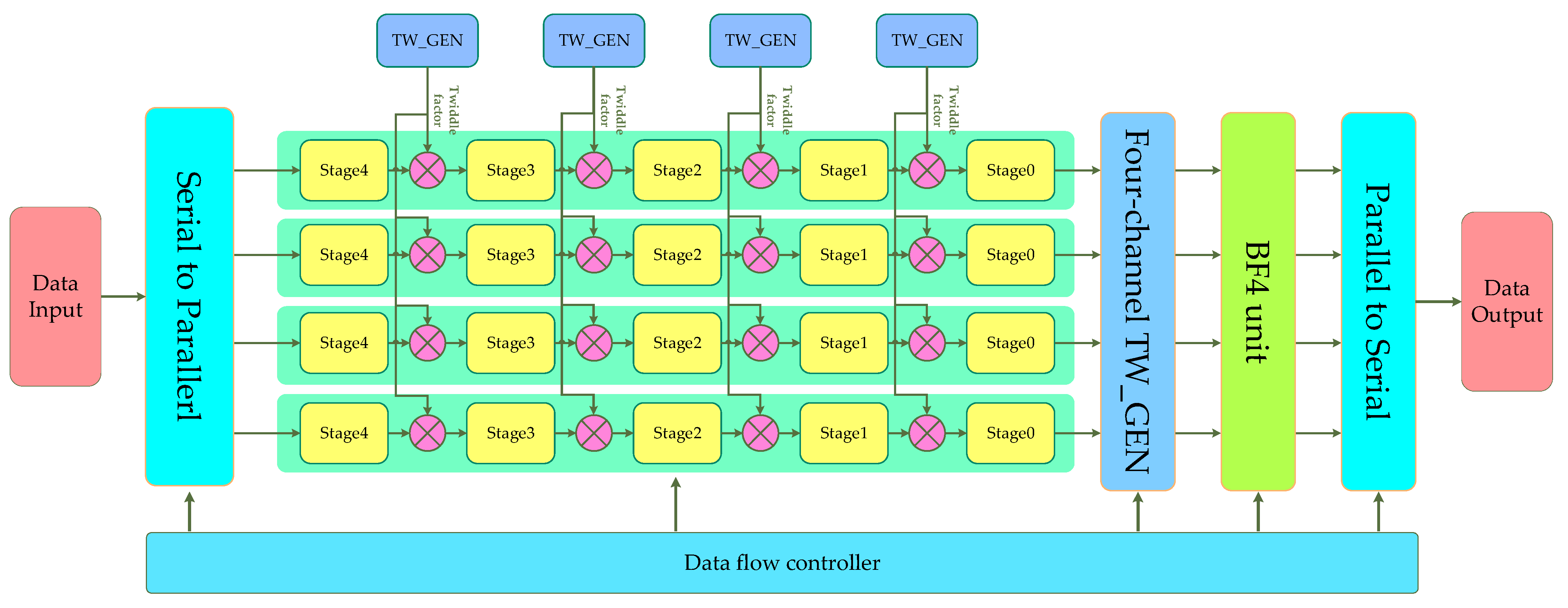
3.4. Four-Channel FFT Processor Structure

Figure 12 shows the design of the four-channel overall scheme using the mixed-radix algorithm. The core of the four-channel processor structure is four single channels. A serial-to-parallel module is set at the front end of the four channels, and a four-channel TW_GEN, BF4 unit and parallel-to-serial module are set at the back of the four channels. A data flow controller is set up to control the addressing and flow control of the entire processor.
The functions and implementation methods of each module in Figure 12 are as follows:
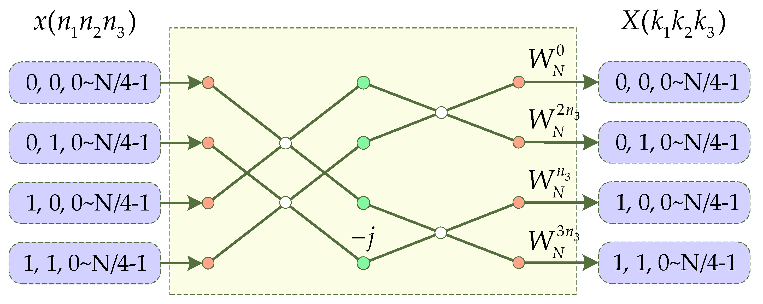
The serial to parallel module is used to decompose the serial data from a single channel into four channels, which can be realized by a multiplexer. In order to ensure the synchronization of the four channels, a buffer unit needs to be set up so that the data of the four channels are sent at the same time. The decomposition rules are shown in Figure 13.
The stage module and TW_GEN are identical to those in the single-channel structure. Since the structure of the four channels is identical, the required twiddle factor after the operation level at the same position is the same, so the four channels can share one TW_GEN after the same operation stage.
The four-channel TW_GEN module is used to generate the twiddle factor in Figure 7, and three CORDIC IP cores need to be called for implementation. Four multipliers are provided in the four-channel TW_GEN module, which is different from the TW_GEN module.
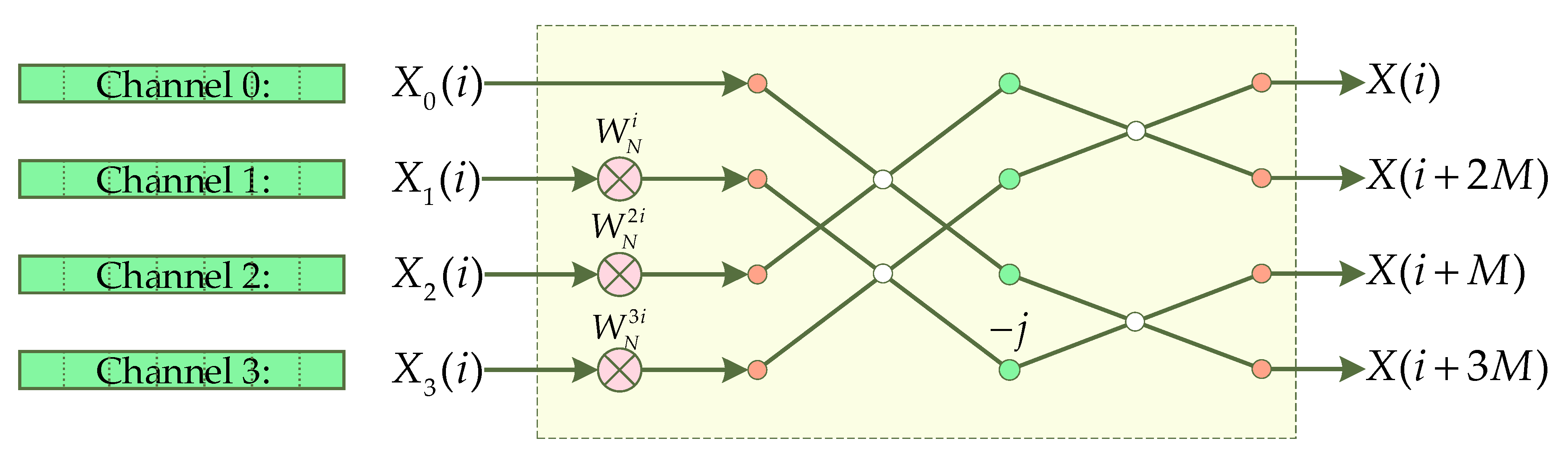
The R4 unit is used to implement the radix-4 algorithm, which integrates the data of the four channels and is implemented by logic circuits.
The parallel-to-serial module is used to combine four channels of data into one channel, and its operation rules are opposite to those of the serial-to-parallel module and can be realized by register groups.
The data flow controller is used to control the data flow in the processor. Its functions include the following: continue to input zero after the end of the data to drive the processor; provide operation addresses for the register groups in the serial-to-parallel module and parallel-to-serial module; provide the x value for the CORDIC core in all TW_GEN modules (including four-channel TW_GEN module), that is, there is no need to set the address controller in each TW_GEN module; and provide the operating address and instructions for the RAM provided in the SDF, and there is also no need to set the address controller separately in the SDF.
The processing flow of the data in the four-channel FFT is as follows. First, the serial time data enter the serial-to-parallel module and are cached, as shown in Figure 13. After a group of caches, the data are synchronously transferred to Stage 4 of the four channels; after the data enter the stage module, they pass through three SDF structures according to the data flow method introduced in Section 2.1, and finally flow out of the stage module. Except for the last stage, the data flowing out of a stage are multiplied with the rotation factor generated by TW_GEN, and then flow into the next stage. After the four data from Stage 0 flow into the four-channel TW in parallel, they are independently multiplied with the twiddle factor, and then flow into the R4 unit in parallel. The data flowing into the R4 unit are processed in parallel according to the structure in Figure 7, and the calculation results flow into the parallel-to-serial module in parallel. Finally, the data are merged into a serial data output by the parallel-to-serial module.

4. Experimental Evaluation and Results

In this section, we evaluated the performance of the proposed design through several experiments. First, we implemented the proposed processor on FPGA. Four sets of experimental data were used to verify the function of the FFT processor, with the accuracy of the calculation results and the real-time performance of the calculation evaluated. Then, the occupation of hardware resources was also evaluated which was compared with other FFT processors. The experimental settings and detailed experimental results are shown below.

4.1. Experimental Settings

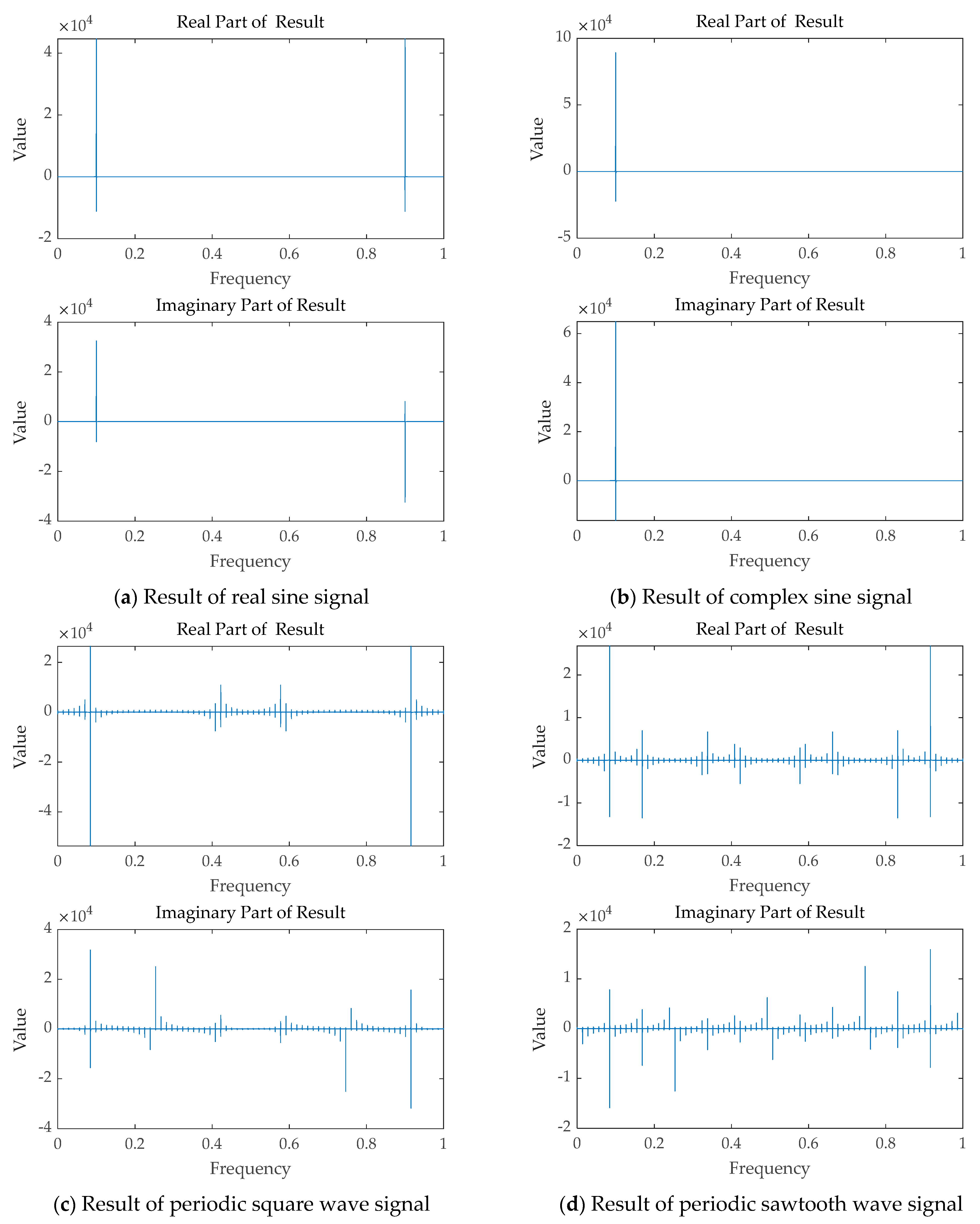
4.1.1. Experimental Data Settings

The proposed processor was used to process 32-bit signed fixed-point numbers without setting integer bits, that is, the range of input data was −1 to 0.9999999995, with the data width of 64bit, since the input data were complex numbers, including real and imaginary parts. The data length was 128 × 1024 points. Therefore, the overall size of the input data was 64 × 124 × 1024 bit = 8 Mbit. Four sets of test signals were selected in the experiment as experimental data, including real sine signal, complex sine signal, periodic square wave signal and periodic sawtooth signal. The function expressions of the four test signals are shown in Table 6; the range of variable t is from 0 to 128 × 1024 − 1. The square function generates a square wave with period 2π for the elements of the time array t. The default amplitude is 1, and the duty cycle is 50%. The sawtooth function generates a sawtooth wave with period 2π for the elements of the time array t. The default amplitude is 1, which linearly changes from −1 to 1 in one cycle.

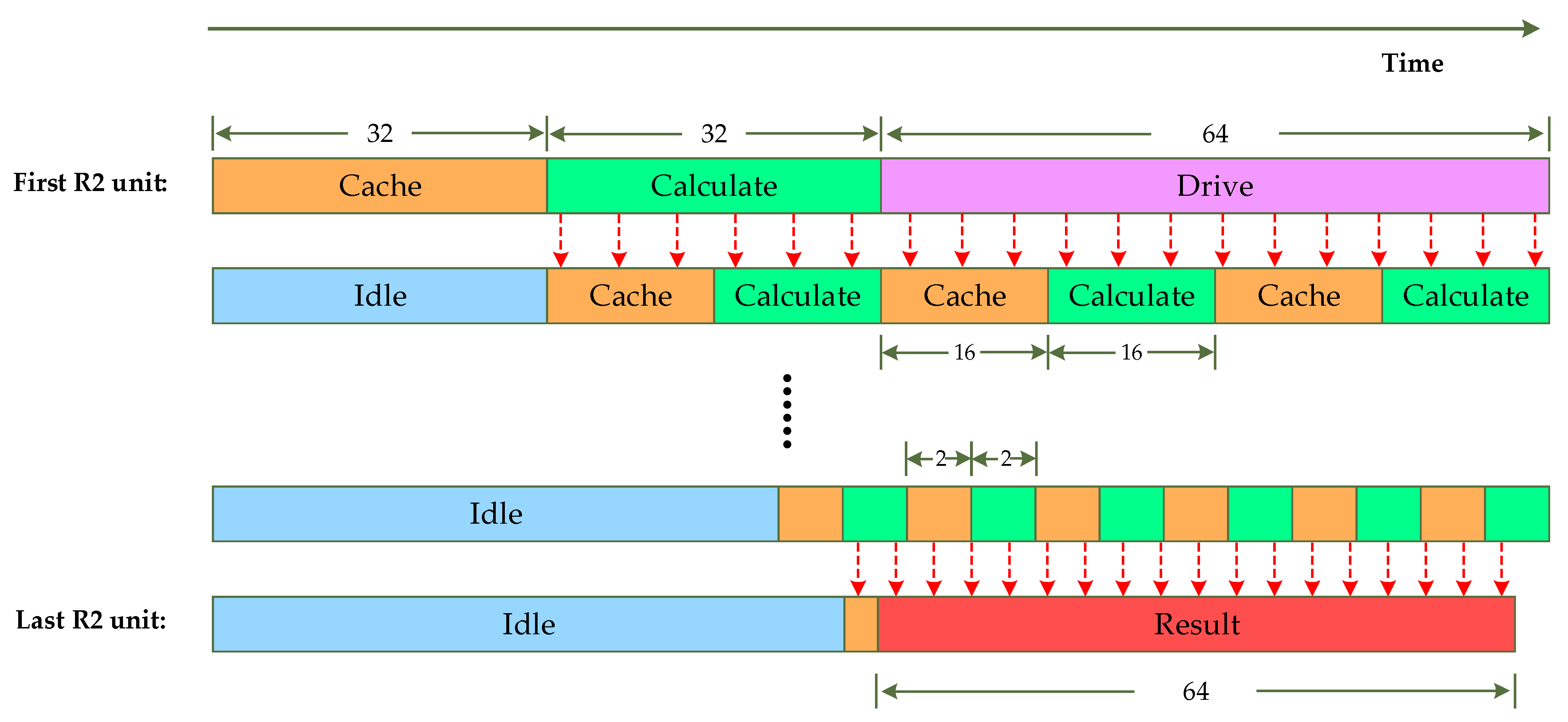
4.1.2. Experimental Procedure

In order to verify the feasibility of the four-channel FFT processor proposed in Section 3, we described the structure of the four-channel FFT processor with Verilog HDL, and synthesized and implemented it on Xilinx Vivado 2018.3. In Vivado 2018.3, we chose the xc7vx690tffg1761-2 board under the Virtex7 series as the hardware platform. First, the test data was generated by Matlab R2019b, and saved in a txt file. Then, Test Bench in Vivado read the data in the txt file and inputted it into the FFT processor. After that, Testbench received the processed results and saved the results to another txt file. Finally, Matlab read the txt file for the saved result, and adjusted the frequency domain order from bit reversed order to natural order.

4.2. Performance Evaluation

In order to evaluate the processing accuracy of the proposed FFT processor, we used the calculation result of the double-precision floating-point number FFT in Matlab as the accurate value for comparison. The width of a double-precision floating-point number was 64-bit, including 52 decimal bits, so its accuracy was considered to be much higher than a 32-bit fixed-point number. Meanwhile, we used the calculation result of single-precision floating-point number FFT in Matlab as a comparison group, which has been widely used in practice. We selected the largest relative error in the calculation result as the standard for evaluating calculation accuracy, because in actual scenes, we often care about the largest value of the data in a frequency domain, which is the main frequency component. If the maximum relative error is small, the result can be guaranteed to have high accuracy near the main frequency component.
Figure 14 shows the frequency domain waveform diagram of the FFT calculation result in FPGA. Each calculation result has been divided into a real part and an imaginary part. Table 7 lists the maximum relative error values of four sets of signals in the 32-bit fixed-point number result implemented by FPGA and single-precision floating-point number result implemented by Matlab. The accuracy of the 32-bit fixed-point number in FPGA was about 10 times higher than the single-precision floating-point number in Matlab, indicating that the proposed FFT processor has better calculation accuracy because the accuracy of the 32-bit fixed-point number was originally higher than the single-precision floating-point numbers. Moreover, according to the fixed-point adjustment proposed in Section 2.2, the width of the fixed-point numbers was constantly expanding, so our data scale was actually larger than the floating-point number, which can be considered as the exchange of hardware resources for improvement of accuracy.
In order to evaluate the real-time performance of the proposed processor, we chose Xilinx LogiCORE IP Fast Fourier Transform v9.1 (xfft 9.1) as a comparison, which was limited by the lack of literature focusing on implementing large point FFT processors on an FPGA device. The maximum transform length supported in xfft 7.1 IP was 65,536; we used the single-channel FFT structure in Section 2.3 as the experimental group. The Xilinx IP can be set to four architectures, including Pipelined: Streaming I/O, Radix-4: Burst I/O, Radix-2: Burst I/O and Radix-2 Lite: Burst I/O. Table 8 lists the transform cycles of the proposed processor and four architectures in Xilinx IP. Compared with the four architectures, the cycles of the proposed FFT processor are slightly smaller than the Pipelined architecture, and far less than the other three architectures, which is acceptable. Obviously, the Pipelined structure has the fastest real-time performance. As for the reason why the cycles of the processor proposed was smaller than the Pipelined structure, we considered that in order to realize the AXI4 interface in Xilinx IP, some handshake signals were added, which also required additional cycles. When the proposed processor works in a four-channel mode, it will achieve 128k-point FFT calculation with almost the same cycles in Table 8 at the cost of nearly four times the hardware resources. In practical applications, we need to make a trade-off between real-time performance and hardware resource consumption.

4.3. Hardware Performance Comparison

In order to evaluate the hardware performance of the proposed processor, we also compared it with some previous work and Xilinx IP. The performance comparison is shown in Table 9, where it is indicated in the relevant references. In the table, BRAM is used for storage, which is often proportional to the size of the data (width × length), and DSP is a multiplier. The real-time performance of Xilinx IP is very close to our design. If we use Xilinx IP to implement 128k point FFT, we need to use at least four identical IPs, that is, the processor will occupy four times the hardware resources as in the table. Therefore, using Xilinx IP to achieve the same function of the processor will require at least 408 DSP and 590 BRAM, which is far larger than our design. In Reference [29], the author proposed an efficient FFT processor which used a method of pre-saving all twiddle factors. Therefore, this FFT processor did not need to generate factors in real time, which saved the use of Slice LUTs resources with a good real-time performance. However, the pre-stored selection factors took up a lot of BRAM resources. When a large-point FFT processor was implemented on FPGA, BRAM resources were the most limited, so this strategy is not suitable. In Reference [31], the author proposed a configurable FFT processor with a 16-bit fixed-point number, so the processor occupied a few BRAM and Slice LUTs. Although the transform length in Reference [31] was longer than that in Reference [29], the FFT processor in Reference [31] still occupied less BRAM. However, a too-small width also brought the problem of insufficient calculation accuracy. In addition, because the Reference [31] adopted the radix-22 algorithm, it obviously took up more DSP per unit transform length, compared with our design. In Reference [32], the author proposed a floating-point FFT processor. Due to the use of floating-point number, the FFT processor can process a wider range of data. However, the use of floating-point numbers may cause the processor to take up more hardware resources than our design, especially in Slice LUTs.

5. Conclusions

In this paper, we proposed a high-speed four-channel 128k-point FFT processor suitable for FPGA implementation. The radix-23 algorithm was used to save multiplier resources, as well as the mixed-radix algorithm to achieve a four-channel parallel processing structure. Then, we adopted a SDF structure to realize pipeline processing. Thus, a fixed-point word length adjustment strategy was proposed to ensure the accuracy of data processing. The proposed FFT processor was implemented on the xc7vx690tffg1761-2 board. Experimental results showed that the proposed processor has high calculation accuracy compared with a single-precision floating-point number, with acceptable real-time performance. Finally, it has high efficiency in the occupation of hardware resources, compared with Xilinx IP and some previous work.

Author Contributions

Conceptualization, Y.L. and H.C.; methodology, Y.L. and Y.X.; software, Y.L., H.C., and Y.X.; validation, Y.L.; formal analysis, Y.L.; investigation, Y.L. and Y.X.; resources, H.C. and Y.X.; writing—original draft preparation, Y.L.; writing—review and editing, Y.L., H.C., and Y.X.; supervision, Y.X.; project administration, H.C.; funding acquisition, H.C. and Y.X. All authors have read and agreed to the published version of the manuscript.

Funding

This research was funded by the National Natural Science Foundation of China under grant no. 91738302.

Acknowledgments

This work was supported by the Chang Jiang Scholars Program under grant T2012122 and the Hundred Leading Talent Project of Beijing Science and Technology under grant Z141101001514005.

Conflicts of Interest

The authors declare no conflict of interest.

References

  1. Wu, C.; Liu, K.Y.; Jin, M. Modeling and a Correlation Algorithm for Spaceborne SAR Signals. IEEE Trans. Aerosp. Electron. Syst. 1982, AES-18, 563–575. [Google Scholar] [CrossRef]
  2. Raney, R.K.; Runge, H.; Bamler, R.; Cumming, I.G.; Wong, F.H. Precision SAR processing using chirp scaling. IEEE Trans. Geosci. Remote Sens. 1994, 32, 786–799. [Google Scholar] [CrossRef]
  3. Meng, J. Research on Vibration and Lever-Arm Effect Influence to Onboard SAR Centre Motion Parameters. In Proceedings of the 2011 Second International Conference on Digital Manufacturing & Automation, Zhangjiajie, China, 5–7 August 2011; pp. 1050–1054. [Google Scholar]
  4. Lou, Y.; Clark, D.; Marks, P.; Muellerschoen, R.J.; Wang, C.C. Onboard Radar Processor Development for Rapid Response to Natural Hazards. IEEE J. Sel. Top. Appl. Earth Obs. Remote Sens. 2016, 9, 2770–2776. [Google Scholar] [CrossRef]
  5. Yan, X.; Chen, J.; Nies, H.; Yang, W.; Loffeld, O. Doppler Parameter Estimation Model Using Onboard Orbit Determination and Inter-satellite Distance Measurement for Spaceborne Bistatic SAR Real-time Imaging. In Proceedings of the 2019 6th Asia-Pacific Conference on Synthetic Aperture Radar (APSAR), Xiamen, China, 26–29 November 2019; pp. 1–4. [Google Scholar]
  6. Seasat. Available online: https://en.wikipedia.org/wiki/Seasat (accessed on 11 February 2021).
  7. KOMPSAT 5 (Arirang 5). Available online: https://space.skyrocket.de/doc_sdat/kompsat-5.htm (accessed on 7 July 2020).
  8. PAZ SAR Satellite Mission of Spain. Available online: https://directory.eoportal.org/web/eoportal/satellite-missions/p/paz (accessed on 1 January 2021).
  9. RCM (RADARSAT Constellation Mission). Available online: https://directory.eoportal.org/web/eoportal/satellite-missions/r/rcm (accessed on 1 January 2021).
  10. China Launches Remote Sensing Satellite Yaogan-33. Available online: https://www.businesstoday.in/current/world/china-launches-remote-sensing-satellite-yaogan-33/story/426233.html (accessed on 29 December 2020).
  11. Capella X-SAR (Synthetic Aperture Radar) Constellation. Available online: https://directory.eoportal.org/web/eoportal/satellite-missions/content/-/article/capella-x-sar (accessed on 1 January 2021).
  12. Synthetic Aperture Radar Gets Boost From Small Satellites. Available online: https://www.csrwire.com/press_releases/708016-synthetic-aperture-radar-gets-boost-small-satellites (accessed on 13 November 2020).
  13. Suess, M.; Schaefer, C.; Zahn, R. Discussion of the introduction of on-board SAR data processing to spaceborne SAR instruments. In Proceedings of the IGARSS 2000—IEEE 2000 International Geoscience and Remote Sensing Symposium. Taking the Pulse of the Planet: The Role of Remote Sensing in Managing the Environment, Proceedings (Cat. No.00CH37120), Honolulu, HI, USA, 24–28 July 2000; Volume 5, pp. 2331–2333. [Google Scholar]
  14. Green, R.C.; Wang, L.; Alam, M. Applications and Trends of High Performance Computing for Electric Power Systems: Focusing on Smart Grid. IEEE Trans. Smart Grid 2013, 4, 922–931. [Google Scholar] [CrossRef]
  15. Hu, W.; Zhang, Y.; Fu, J. An introduction to CPU and DSP design in China. Sci. China Inf. Sci. 2016, 59, 1–8. [Google Scholar] [CrossRef]
  16. ASIC or FPGA? Each Solution Has Advantages and Disadvantages. Available online: https://www.swindonsilicon.com/asic-fpga-advantages-and-disadvantages/ (accessed on 12 October 2018).
  17. Ploeg, A.V.D. Why Use an FPGA Instead of a CPU or GPU? Available online: https://blog.esciencecenter.nl/why-use-an-fpga-instead-of-a-cpu-or-gpu-b234cd4f309c (accessed on 14 August 2018).
  18. Paek, S.W.; Balasubramanian, S.; Kim, S.; De Weck, O. Small-Satellite Synthetic Aperture Radar for Continuous Global Biospheric Monitoring: A Review. Remote Sens. 2020, 12, 2546. [Google Scholar] [CrossRef]
  19. Fu, W.; Ma, J.; Chen, P.; Chen, F. Remote Sensing Satellites for Digital Earth. In Manual of Digital Earth; Guo, H., Goodchild, M.F., Annoni, A., Eds.; Springer: Singapore, 2020; pp. 55–123. [Google Scholar]
  20. Zhou, X.; Xie, Y.; Yang, C.; Du, Q.; Deng, Y. Fixed-point simulation technology for SAR real-time imaging system. In Proceedings of the IET International Radar Conference 2015, Hangzhou, China, 14–16 October 2015; pp. 1–5. [Google Scholar]
  21. Palsodkar, P.; Gurjar, A. Improved fused floating point add-subtract and multiply-add unit for FFT implementation. In Proceedings of the 2014 2nd International Conference on Devices, Circuits and Systems (ICDCS), Coimbatore, India, 6–8 March 2014; pp. 1–5. [Google Scholar]
  22. Chen, J.; Lei, Y.; Peng, Y.; He, T.; Deng, Z. Configurable floating-point FFT accelerator on FPGA based multiple-rotation CORDIC. Chin. J. Electron. 2016, 25, 1063–1070. [Google Scholar] [CrossRef]
  23. Prabhu, E.; Mangalam, H.; Karthick, S. Design of area and power efficient Radix-4 DIT FFT butterfly unit using floating point fused arithmetic. J. Cent. South Univ. 2016, 23, 1669–1681. [Google Scholar] [CrossRef]
  24. Shaditalab, M.; Bois, G.; Sawan, M. Self-sorting radix-2 FFT on FPGAs using parallel pipelined distributed arithmetic blocks. In Proceedings of the IEEE Symposium on FPGAs for Custom Computing Machines (Cat. No.98TB100251), Napa Valley, CA, USA, 17 April 1998; pp. 337–338. [Google Scholar]
  25. Sun, Z.; Liu, X.; Ji, Z. The Design of Radix-4 FFT by FPGA. In Proceedings of the 2008 International Symposium on Intelligent Information Technology Application Workshops, Shanghai, China, 21–22 December 2008; pp. 765–768. [Google Scholar]
  26. Chandu, Y.; Maradi, M.; Manjunath, A.; Agarwal, P. Optimized High Speed Radix-8 FFT Algorithm Implementation on FPGA. In Proceedings of the 2018 2nd International Conference on Trends in Electronics and Informatics (ICOEI), Tirunelveli, India, 11–12 May 2018; pp. 430–435. [Google Scholar]
  27. Santhosh, L.; Thomas, A. Implementation of radix 2 and radix 22 FFT algorithms on Spartan6 FPGA. In Proceedings of the 2013 Fourth International Conference on Computing, Communications and Networking Technologies (ICCCNT), Tiruchengode, India, 4–6 July 2013; pp. 1–4. [Google Scholar]
  28. Tang, J.; Li, X.; Zhang, G.; Lai, Z. Design of high-throughput mixed-radix MDF FFT processor for IEEE 802.11.3c. In Proceedings of the 2012 IEEE 11th International Conference on Solid-State and Integrated Circuit Technology, Xi’an, China, 29 October–1 November 2012; pp. 1–3. [Google Scholar]
  29. Chen, Y.; He, C. A efficient design of a real-time FFT architecture based on FPGA. In Proceedings of the IET International Radar Conference, Xi’an, China, 14–16 April 2013; pp. 1–5. [Google Scholar]
  30. Cumming, I.; Wong, F.; Raney, K. A SAR Processing Algorithm with No Interpolation. In Proceedings of the IGARSS′92 International Geoscience and Remote Sensing Symposium, Houston, TX, USA, 26–29 May 1992; pp. 376–379. [Google Scholar]
  31. Yang, C.; Xie, Y.; Chen, L.; Chen, H.; Deng, Y. Design of a configurable fixed-point FFT processor. In Proceedings of the IET International Radar Conference, Hangzhou, China, 14–16 October 2015; pp. 1–4. [Google Scholar]
  32. Zhou, J.; Dong, Y.; Dou, Y.; Lei, Y. Dynamic Configurable Floating-Point FFT Pipelines and Hybrid-Mode CORDIC on FPGA. In Proceedings of the 2008 International Conference on Embedded Software and Systems, Chengdu, China, 29–31 July 2008; pp. 616–620. [Google Scholar]
Figure 1. The flowchart of the standard chirp-scaling (CS) algorithm.
Electronics 10 00816 g001
Figure 2. The flowchart of the standard CS algorithm.
Electronics 10 00816 g002
Figure 3. Implementation structure of terms ( 1 ) n 1 k 1 , ( 1 ) n 2 k 2 and ( 1 ) n 3 k 3 .
Electronics 10 00816 g003
Figure 4. Implementation structure diagram of the radix-23 algorithm.
Electronics 10 00816 g004
Figure 5. Structure diagram of the radix-4 algorithm.
Electronics 10 00816 g005
Figure 6. Flowchart of the radix-22 algorithm.
Electronics 10 00816 g006
Figure 7. Flowchart of a four-channel algorithm.
Electronics 10 00816 g007
Figure 8. 64-Point radix-23 (R-23) single-path delay feedback (SDF) structure diagram.
Electronics 10 00816 g008
Figure 9. Schematic diagram of pipelined processing of each radix-2 butterfly unit (BF2).
Electronics 10 00816 g009
Figure 10. Data word length adjustment strategy for a radix-23 butterfly unit.
Electronics 10 00816 g010
Figure 11. Single channel structure and its sub-modules.
Electronics 10 00816 g011
Figure 12. Four-channel 128k point FFT overall structure diagram.
Electronics 10 00816 g012
Figure 13. Serial to parallel module decomposition rules.
Electronics 10 00816 g013
Figure 14. Frequency domain diagram of the results of four test signals calculated by Field Programmable Gate Array (FPGA).
Electronics 10 00816 g014
Table 1. Summary of the model and resolution of each Synthetic Aperture Radar (SAR) satellite.
Satellite NameCountryLaunch TimeWorking Mode and Resolution
ERS-1ESA1991Stripmap mode, 20 m
ALOSJapan2006Spotlight mode, 2.5 m
Yaogan14China2012Spotlight mode, 0.5 m
KOMPSat-5Korea2013Spotlight mode, 1 m
Strip mode, 3 m
Scan mode, 10 m
ALOS-2Japan2014Spotlight mode, 1 × 3 m
Stripmap mode, 3/6/10 m
Scan model, 100 m
PazSpain2016Spotlight mode, 2 m
Stripmap mode, 6 m
Scan model, 15 m
Capela1USA2018Spotlight mode, 0.3–1 m
RCM 1, 1, 2Canada2019Spotlight mode, 1–1.3 m
Capella 2, 3, 4USA2021Spotlight mode, 0.3–1 m
Table 2. Summary of the Fast Fourier transform (FFT)/inverse FFT (IFFT) operation.
StepNumber of
Multiplication
Number of
Addition
Number of
Computation
Step 1 2 N r N a ( log 2 N r 1 ) N r N a ( log 2 N r 1 ) + 2 N r N a log 2 N r 3 N r N a ( log 2 N r 1 ) + 2 N r N a log 2 N r
Step 3 2 N r N a ( log 2 N a 1 ) N r N a ( log 2 N a 1 ) + 2 N r N a log 2 N a 3 N r N a ( log 2 N a 1 ) + 2 N r N a log 2 N a
Step 5 2 N r N a ( log 2 N a 1 ) N r N a ( log 2 N a 1 ) + 2 N r N a log 2 N a 3 N r N a ( log 2 N r 1 ) + 2 N r N a log 2 N r
Step 7 2 N r N a ( log 2 N r 1 ) N r N a ( log 2 N r 1 ) + 2 N r N a log 2 N r 3 N r N a ( log 2 N r 1 ) + 2 N r N a log 2 N r
Total 4 N r N a ( log 2 N r 1 ) + 4 N r N a ( log 2 N a 1 ) 2 N r N a ( log 2 N r 1 ) + 2 N r N a ( log 2 N a 1 ) + 4 N r N a log 2 N r + 4 N r N a log 2 N a 6 N r N a ( log 2 N r 1 ) + 6 N r N a ( log 2 N a 1 ) + 4 N r N a log 2 N r + 4 N r N a log 2 N a
Table 3. Summary of phase factor complex multiplication operation.
StepNumber of
Multiplication
Number of
Addition
Number of
Computation
Step 2 4 N r N a 2 N r N a 6 N r N a
Step 4 4 N r N a 2 N r N a 6 N r N a
Step 6 4 N r N a 2 N r N a 6 N r N a
Total 12 N r N a 6 N r N a 18 N r N a
Table 4. Comparison of hardware unit usage of radix-2 (R-2), radix-4 (R-4), and radix-23 (R-23) algorithms.
AlgorithmOccupancy for
Multiplier
Occupancy for
Memory
Occupancy for
Butterfly Unit
R-2 SDF log 2 N 2 N 1 log 2 N ( R 2 )
R-4 SDF log 4 N 1 N 1 log 4 N ( R 4 )
R-23 SDF log 8 N 1 N 1 log 2 N ( R 2 )
Table 5. The change value of each parameter in Equation (11) in one period.
ParameterTW_GEN4TW_GEN3TW_GEN2TW_GEN1
N 32,758409651264
n 4 0, 1, 2, …, 40950, 1, 2, …, 5110, 1, 2, …, 630, 1, 2, …, 7
k 1 + 2 k 2 + k 3 0, 4, 2, 6, 1, 5, 3, 70, 4, 2, 6, 1, 5, 3, 70, 4, 2, 6, 1, 5, 3, 70, 4, 2, 6, 1, 5, 3, 7
Table 6. Function expressions of four test signals.
Name of Test SignalFunction Expressions of Test Signal
Real sine signal 0.9 × sin ( 2 π × 0.1 × t )
Complex sine signal 0.9 × exp ( j × 2 π × 0.1 × t )
Periodic square wave signal 0.9 × square ( 100 × t )
Periodic sawtooth signal 0.9 × sawtooth ( 100 × t )
Table 7. Maximum relative error of 32-bit fixed-point number on FPGA and single-precision floating-point number on Matlab.
Real Sine SignalComplex Sine SignalSquare Save SignalSawtooth Wave Signal
32-bit Fixed-point1.84 × 10−46.05 × 10−44.18 × 10−43.05 × 10⁻⁴
Single-precision Floating-point1.25 × 10−45.1 × 10−44.8 × 10−42.2 × 10⁻⁴
Table 8. Transform cycles of the proposed processor and four architectures in Xilinx IP.
ProposedPipelinedRadix-4Radix-2Radix-2 Lite
Transform cycles131,218131,284262,367655,7411,179,691
Table 9. The performance comparison of our design and previous works.
Our DesignXilinx IP[29][31][32]
Transform length128k64k25610244k
Data type32-bit fixed32-bit fixed24-bit fixed16-bit fixed32-bit floating
Transform cycles131,218131,28429848-
Slice LUTs39,51911,1826043517444,071
BRAM Tiles282147.584179
DSPs1461022416200
Publisher’s Note: MDPI stays neutral with regard to jurisdictional claims in published maps and institutional affiliations.

